EP1265344A2 - Switching power supply - Google Patents
Switching power supply Download PDFInfo
- Publication number
- EP1265344A2 EP1265344A2 EP02253943A EP02253943A EP1265344A2 EP 1265344 A2 EP1265344 A2 EP 1265344A2 EP 02253943 A EP02253943 A EP 02253943A EP 02253943 A EP02253943 A EP 02253943A EP 1265344 A2 EP1265344 A2 EP 1265344A2
- Authority
- EP
- European Patent Office
- Prior art keywords
- power supply
- signal
- switching
- output
- voltage
- Prior art date
- Legal status (The legal status is an assumption and is not a legal conclusion. Google has not performed a legal analysis and makes no representation as to the accuracy of the status listed.)
- Withdrawn
Links
Images
Classifications
-
- H—ELECTRICITY
- H02—GENERATION; CONVERSION OR DISTRIBUTION OF ELECTRIC POWER
- H02M—APPARATUS FOR CONVERSION BETWEEN AC AND AC, BETWEEN AC AND DC, OR BETWEEN DC AND DC, AND FOR USE WITH MAINS OR SIMILAR POWER SUPPLY SYSTEMS; CONVERSION OF DC OR AC INPUT POWER INTO SURGE OUTPUT POWER; CONTROL OR REGULATION THEREOF
- H02M3/00—Conversion of DC power input into DC power output
- H02M3/02—Conversion of DC power input into DC power output without intermediate conversion into AC
- H02M3/04—Conversion of DC power input into DC power output without intermediate conversion into AC by static converters
- H02M3/10—Conversion of DC power input into DC power output without intermediate conversion into AC by static converters using discharge tubes with control electrode or semiconductor devices with control electrode
- H02M3/145—Conversion of DC power input into DC power output without intermediate conversion into AC by static converters using discharge tubes with control electrode or semiconductor devices with control electrode using devices of a triode or transistor type requiring continuous application of a control signal
- H02M3/155—Conversion of DC power input into DC power output without intermediate conversion into AC by static converters using discharge tubes with control electrode or semiconductor devices with control electrode using devices of a triode or transistor type requiring continuous application of a control signal using semiconductor devices only
- H02M3/156—Conversion of DC power input into DC power output without intermediate conversion into AC by static converters using discharge tubes with control electrode or semiconductor devices with control electrode using devices of a triode or transistor type requiring continuous application of a control signal using semiconductor devices only with automatic control of output voltage or current, e.g. switching regulators
-
- H—ELECTRICITY
- H02—GENERATION; CONVERSION OR DISTRIBUTION OF ELECTRIC POWER
- H02M—APPARATUS FOR CONVERSION BETWEEN AC AND AC, BETWEEN AC AND DC, OR BETWEEN DC AND DC, AND FOR USE WITH MAINS OR SIMILAR POWER SUPPLY SYSTEMS; CONVERSION OF DC OR AC INPUT POWER INTO SURGE OUTPUT POWER; CONTROL OR REGULATION THEREOF
- H02M1/00—Details of apparatus for conversion
- H02M1/32—Means for protecting converters other than automatic disconnection
Definitions
- the present invention relates to a switching power supply, which can regulate the amount of limitation of power supply output power according to the input or output of the switching power supply and diminish overshoot of inrush current and output voltage during starting.
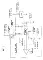
- the example of the prior art shown in Fig. 2 is a step-down chopper that uses pulse width modulation (to be abbreviated as PWM), and is composed of switching element 1 that generates a pulse voltage by switching the input voltage, smoothing device 2 that smoothes said pulse voltage, detection device 3 that detects power supply output voltage 16, power supply output current 17 or both, switching signal generation device 4 that receives the signal detected by this detection device 3 and generates a drive signal of switching element 1, and soft start circuit 11 that generates a soft start signal.
- PWM pulse width modulation
- switching signal generation device 4 is provided error amplifier 8 that compares power supply output voltage 16 with a reference voltage 14 and transmits a signal in which that error is amplified, and PWM modulator 9 that performs pulse width modulation of the signal transmitted by this error amplifier 8.
- soft start circuit 11 is composed by connecting a constant voltage source like reference voltage 14, resistor 12 and capacitor 13 in series.
- Power supply output voltage 16 is compared with reference voltage 14, the error amplification signal voltage of those compared voltages is subjected to pulse width modulation by using as the input voltage of PWM modulator 9, switching element 1 is switched according to the output signal of this modulator 9, and the output of this switching element 1 is input to smoothing circuit 2 to be able to obtain power supply output voltage 16.
- PWM functions so as to supply large electrical power to the load by increasing the pulse width, namely by increasing the duty, when a large power supply output current 17 is required, and reduce electrical power to the load by decreasing the duty when power supply output current 17 is small.
- PWM modulator 9 that performs PWM is composed of a comparator having three inputs for a chopping wave that serves as a reference, an error amplification signal voltage and a soft start signal, and realizes PWM was realized by comparing the signal of the lower voltage valve between the error amplification signal voltage and soft start signal with the chopping wave.
- This example of the prior art is equipped with a typical soft start circuit 11, accumulation of charge in the above capacitor begins from the time the power supply is started, and a soft start signal is generated by gradually increasing the voltage of the terminals connecting the above resistor 12 and the above capacitor 13 over an amount of time determined by the product of the value of the above resistor 12 and the value of the above capacitor 13.
- the object of the invention is to provide a switching power supply that is capable of limiting the power supply output power using a method that is compatible with compact size regardless of the modulation system.
- the invention according to a first aspect of the present invention relates to a switching power supply that is capable of regulating the limit of power supply output power as desired by applying a pulse signal to a switching element that forcibly switches off that switching element according to a signal obtained by detecting the input voltage, output voltage, input current or output current of the power supply.
- the switching power supply according to the present invention is provided with a switching element that converts an input voltage to a pulse voltage, the output of this switching element is provided with a smoothing device for smoothing the above pulse voltage, and the output of this smoothing device is composed so as to be connected to a load in the form of the power supply output.
- the above switching power supply is provided with a detection device that detects the power supply output voltage, power supply output current or both, and is equipped with a switching signal generation device for generating a switching element drive signal according to the detected signal.
- the output of the above switching signal generation device is connected to one input of a reset device that is able to switch off the switching element regardless of the signal of the switching signal generation device, and is connected to the switching element.
- the other input of the above reset device is connected to the output of a pulse signal generation device that receives a signal from a control signal detection device that detects at least one of input voltage, input current, output voltage or output current, and generates a signal for reset, and is capable of regulating the limit of power supply output power by changing the duty of the above pulse signal.
- the power supply output power limit can also be regulated by inputting a signal that has detected either power supply internal voltage or power supply internal current in the form of a power supply internal signal such as a reference voltage, in addition to the above detection signal, to the above reset device input.
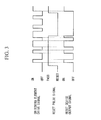
- Fig. 3 indicates the relationship among the drive signal of a switching element, pulse signal for resetting, and reset device output signal, and the switching element drive signal drives the switching element as is when the reset pulse signal passes through, while a signal that switches off the switching element is applied to the switching element when the reset pulse signal is reset.
- the maximum value of the duty of the reset device output signal is determined by the duty of the reset pulse regardless of the switching element drive signal, and since that maximum value cannot be equal to or greater than the duty of the reset pulse, the power supply output power can be limited.
- the magnitude of power limitation can be regulated as desired by changing the duty of the reset pulse between 0% and 100%.
- soft starting of the power supply can be realized by gradually changing the duty of the reset pulse together with starting of the power supply, and gradually decreasing the amount of power limitation.
- a pulse signal generation device for realizing the above soft start can be realized by using a resistor and capacitor similar to those of conventional methods, differing from conventional methods, it can also be realized with a simple logic circuit without using a capacitor, thereby enabling a higher level of integration and compact size.
- the reset device is provided after the switching signal generation device in the present invention, limitation of output power can be realized regardless of the modulation system within the switching signal generation device.
- the present invention allows power supply output power to be regulated regardless of the modulation system used for power supply control by changing the duty of the reset pulse signal, thereby making it possible to provide a compact switching power supply free of inrush current and overshoot.
- the amount of limitation of power supply output power can be regulated by changing the duty of a reset pulse signal applied to a reset device that resets the switching element drive signal, thereby making it possible to provide a compact switching power supply that is free of inrush current and overshoot during starting in the case of adapting to soft starting during power supply starting.
- a switching power supply can be provided that allows power supply output power to be regulated by various modulation systems without being affected by the type of modulation system by providing the reset device after the switching signal generation device output.
- a switching power supply can be provided that enables the amount of limitation of power supply output power to be changed gradually in the manner of, for example, a soft start circuit.
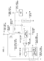
- Fig. 1 shows an embodiment of the present invention
- Fig. 1 is a block drawing of that embodiment.
- the embodiment of Fig. 1 is a step-down chopper power supply that is a type of switching power supply, and is provided with a switching element 1 that generates a pulse voltage by switching the input voltage, a smoothing device 2 that smoothes the pulse voltage, a detection device 3 that detects output voltage, output current or both, a switching signal generation device 4 that receives a signal detected by the detection device 3 and generates a drive signal of the switching element 1, a reset device 5 that switches off the above switching element 1 by resetting the drive signal, a pulse signal generation device 6 that generates a pulse signal for performing resetting, and a control signal detection device 7 that detects at least one of input voltage, input current, output voltage or output current in order to obtain a signal for controlling this pulse signal generation device 6.
- error amplifier 8 which compares power supply output voltage 16 and reference voltage 14 and then transmits a signal in which that error is amplified
- PWM modulator 9 which performs pulse width modulation on the signal transmitted by this error amplifier 8, are provided in switching signal generation device 4.
- the switching power supply of the present invention operates in the manner described below.
- Power supply output voltage 16 is compared with reference voltage 14, and the signal in which that error has been amplified is subjected to pulse width modulation as the input voltage of PWM modulator 9 followed by sending of the switching element drive signal to the input of reset device 5.
- switching element 1 is switched by the output signal of PWM modulator 9, and a constant voltage output can be obtained by inputting the output of this switching element 1 to smoothing circuit 2.
- a signal from control signal detection device 7 that detects power supply input voltage 15 is input to reset signal generation logic circuit 10 provided in reset device 5, enabling a reset signal to be generated according to the input voltage.
- the present embodiment is composed so that the amount of limitation of power supply output power is regulated as desired by pulse signal generation device 6 receiving a signal from control signal detection device 7 that detects a signal like that of power supply input voltage 15, and generating a pulse signal for which the duty is between 0% and 100%, thereby making it possible to gradually change the amount of limitation of power supply output power in the manner of, for example, a soft start circuit.
- soft starting can be realized by detecting starting of the power supply from control signal detection device 7, gradually changing the reset signal applied to reset device 5 from a signal having a large reset duty to a signal having a small reset duty in reset signal generation logic circuit 10 in accordance with starting of the power supply, and then reducing the reset duty to 0% when starting is completed.
- power supply output voltage 16 is detected in control signal detection device 7 in the embodiment shown in Fig. 1, similar effects can also be obtained by detecting either the voltage or current signal of power supply input or output, and in the present embodiment, in addition to the input and output of the power supply, effects can be obtained that are similar to the case of detecting power supply output voltage 16 even if a power supply internal signal such as the output voltage of error amplifier 8 is used.
- input voltage, input current, output voltage and output current include not only the input and output of the power supply, but also that within the power supply.
- a power supply output abnormality protection circuit can also be composed by detecting a power supply output abnormality by detecting output current or output voltage, generating a reset signal that is applied to reset device 5 in accordance with the above abnormality detection signal with pulse signal generation device 6, and regulating limitation of power supply output power with reset device 5.
- the input of reset device 5 is connected to the output of switching signal generation device 4, while the output of the above reset device 5 is connected to switching element 1.
Landscapes
- Engineering & Computer Science (AREA)
- Power Engineering (AREA)
- Dc-Dc Converters (AREA)
Abstract
Description
Claims (4)
- A switching power supply comprising:a switching element (1) that generates a pulse voltage by switching an input voltage, a smoothing device (2) that smoothes said pulse voltage;a detection device (3) that detects an output voltage, output current or both;a switching signal generation device (4) that receives a signal detected by said detection device (3) and generates a drive signal of said switching element (1);a reset device (5) that switches off said switching element (1) by resetting said drive signal;a pulse signal generation device (6) that generates a pulse signal for performing that reset; anda control signal detection device (7) that detects at least one of input voltage, input current, output voltage or output current to obtain a signal for controlling said pulse signal generation device (6).
- The switching power supply according to claim 1 wherein, the output of said switching signal generation device (4) is connected to the input of said reset device (5), and the output of said reset device (5) is connected to said switching element (1).
- The switching power supply according to claim 1 wherein, said pulse signal generation device (6) generates a pulse signal having a duty of between 0% and 100% by receiving a signal from said control signal detection device (7), and is composed so as to generate a signal having a large duty in the case of desiring to limit the output power of the power supply by a large amount, or generate a signal having a small duty in the case of desiring to limit the output power of the power supply by a small amount.
- The switching power supply according to claim 2 wherein, said pulse signal generation device (6) generates a pulse signal having a duty of between 0% and 100% by receiving a signal from said control signal detection device (7), and is composed so as to generate a signal having a large duty in the case of desiring to limit the output power of the power supply by a large amount, or generate a signal having a small duty in the case of desiring to limit the output power of the power supply by a small amount.
Applications Claiming Priority (2)
| Application Number | Priority Date | Filing Date | Title |
|---|---|---|---|
| JP2001172623A JP2002369509A (en) | 2001-06-07 | 2001-06-07 | Switching power unit |
| JP2001172623 | 2001-06-07 |
Publications (2)
| Publication Number | Publication Date |
|---|---|
| EP1265344A2 true EP1265344A2 (en) | 2002-12-11 |
| EP1265344A3 EP1265344A3 (en) | 2004-12-29 |
Family
ID=19014212
Family Applications (1)
| Application Number | Title | Priority Date | Filing Date |
|---|---|---|---|
| EP02253943A Withdrawn EP1265344A3 (en) | 2001-06-07 | 2002-06-06 | Switching power supply |
Country Status (3)
| Country | Link |
|---|---|
| US (1) | US6650099B2 (en) |
| EP (1) | EP1265344A3 (en) |
| JP (1) | JP2002369509A (en) |
Cited By (1)
| Publication number | Priority date | Publication date | Assignee | Title |
|---|---|---|---|---|
| FR2875651A1 (en) * | 2004-09-17 | 2006-03-24 | Johnson Contr Automotive Elect | DC / DC VOLTAGE CONVERTER WITH LIMITED CURRENT SETTING |
Families Citing this family (5)
| Publication number | Priority date | Publication date | Assignee | Title |
|---|---|---|---|---|
| AT410619B (en) * | 2000-07-14 | 2003-06-25 | Siemens Ag Oesterreich | METHOD FOR DETECTING AND / OR LIMITING THE SHORT CIRCUIT STATES OF A SWITCHING CONVERTER |
| JP4523330B2 (en) * | 2004-05-11 | 2010-08-11 | 株式会社リコー | Power supply circuit and equipment having the power supply circuit |
| US6969977B1 (en) * | 2004-06-10 | 2005-11-29 | National Semiconductor Corporation | Soft-start voltage regulator circuit |
| US7239257B1 (en) * | 2005-10-03 | 2007-07-03 | Zilker Labs, Inc. | Hardware efficient digital control loop architecture for a power converter |
| US8237419B2 (en) * | 2009-02-27 | 2012-08-07 | Schneider Electric USA, Inc. | Microcontroller operated current limited switching power supply for circuit protective devices |
Family Cites Families (11)
| Publication number | Priority date | Publication date | Assignee | Title |
|---|---|---|---|---|
| US4236198A (en) * | 1977-12-16 | 1980-11-25 | Sony Corporation | Switching regulator |
| JPH07110132B2 (en) * | 1991-08-22 | 1995-11-22 | 日本モトローラ株式会社 | Voltage converter |
| US5371667A (en) * | 1993-06-14 | 1994-12-06 | Fuji Electrochemical Co., Ltd. | Electric power supply |
| IT1268472B1 (en) | 1993-10-22 | 1997-03-04 | St Microelectronics Srl | BUCK CONVERTER WITH OPERATING MODE AUTOMATICALLY DETERMINED BY THE LOAD LEVEL |
| US5625279A (en) * | 1996-03-28 | 1997-04-29 | Hewlett-Packard Company | DC-DC converter with dynamically adjustable characteristics |
| JP3573888B2 (en) * | 1996-11-27 | 2004-10-06 | 日本テキサス・インスツルメンツ株式会社 | Power supply drive |
| KR19990035769U (en) * | 1998-02-09 | 1999-09-15 | 윤종용 | Power supply with power factor correction circuit |
| US6307356B1 (en) * | 1998-06-18 | 2001-10-23 | Linear Technology Corporation | Voltage mode feedback burst mode circuit |
| JP2001078439A (en) * | 1999-09-06 | 2001-03-23 | Murata Mfg Co Ltd | Switching power supply device |
| EP1199789A1 (en) * | 2000-10-19 | 2002-04-24 | Semiconductor Components Industries, LLC | Circuit and method of operating a low-noise, on-demand regulator in switched or linear mode |
| US6531854B2 (en) * | 2001-03-30 | 2003-03-11 | Champion Microelectronic Corp. | Power factor correction circuit arrangement |
-
2001
- 2001-06-07 JP JP2001172623A patent/JP2002369509A/en active Pending
-
2002
- 2002-06-06 EP EP02253943A patent/EP1265344A3/en not_active Withdrawn
- 2002-06-07 US US10/163,451 patent/US6650099B2/en not_active Expired - Fee Related
Cited By (1)
| Publication number | Priority date | Publication date | Assignee | Title |
|---|---|---|---|---|
| FR2875651A1 (en) * | 2004-09-17 | 2006-03-24 | Johnson Contr Automotive Elect | DC / DC VOLTAGE CONVERTER WITH LIMITED CURRENT SETTING |
Also Published As
| Publication number | Publication date |
|---|---|
| US6650099B2 (en) | 2003-11-18 |
| EP1265344A3 (en) | 2004-12-29 |
| US20020185996A1 (en) | 2002-12-12 |
| JP2002369509A (en) | 2002-12-20 |
Similar Documents
| Publication | Publication Date | Title |
|---|---|---|
| US5459652A (en) | Boot strap circuit for power up control of power supplies | |
| JP4295120B2 (en) | Power supply device having a plurality of switching power supplies connected in parallel | |
| US7071667B2 (en) | DC—DC converter | |
| US9444246B2 (en) | Power converter with switching element | |
| US10680157B2 (en) | Driving system for piezoelectric pump | |
| US20040051513A1 (en) | Switching regulator with dynamic current limiting and drive circuit for the switching regulator | |
| US6621257B2 (en) | DC-DC converter | |
| US20030002298A1 (en) | Power conversion device | |
| US20080224749A1 (en) | System and method for providing stable control for power systems | |
| WO2009155540A1 (en) | Charge pumps with controlled ramp rate | |
| CN110752742A (en) | Direct current conversion control circuit and method for reducing power consumption and power supply system | |
| EP1952213B1 (en) | Buck dc to dc converter and method | |
| US6650099B2 (en) | Switching power supply | |
| JP2003009535A5 (en) | ||
| US20010019492A1 (en) | Efficient, dual-source, wide-input range, isolated DC-DC converter with effective current limit | |
| US5394076A (en) | Pulse width modulated power supply operative over an extended input power range without output power dropout | |
| US6664660B2 (en) | Parallel power supply system with over-voltage protection circuit | |
| KR102073697B1 (en) | Plasma pulse power supply | |
| JP3721825B2 (en) | Power supply | |
| US6801063B1 (en) | Charge compensated bootstrap driving circuit | |
| JPH1141914A (en) | DC-DC converter | |
| JPH10309078A (en) | Switching type DC power supply | |
| US12261531B2 (en) | Buck-boost converter for contactor drive | |
| JP2859022B2 (en) | Power control system | |
| JP4312941B2 (en) | Solenoid drive pump control circuit |
Legal Events
| Date | Code | Title | Description |
|---|---|---|---|
| PUAI | Public reference made under article 153(3) epc to a published international application that has entered the european phase |
Free format text: ORIGINAL CODE: 0009012 |
|
| AK | Designated contracting states |
Kind code of ref document: A2 Designated state(s): AT BE CH CY DE DK ES FI FR GB GR IE IT LI LU MC NL PT SE TR |
|
| AX | Request for extension of the european patent |
Free format text: AL;LT;LV;MK;RO;SI |
|
| PUAL | Search report despatched |
Free format text: ORIGINAL CODE: 0009013 |
|
| AK | Designated contracting states |
Kind code of ref document: A3 Designated state(s): AT BE CH CY DE DK ES FI FR GB GR IE IT LI LU MC NL PT SE TR |
|
| AX | Request for extension of the european patent |
Extension state: AL LT LV MK RO SI |
|
| 17P | Request for examination filed |
Effective date: 20050404 |
|
| AKX | Designation fees paid |
Designated state(s): AT BE CH CY DE DK ES FI FR GB GR IE IT LI LU MC NL PT SE TR |
|
| STAA | Information on the status of an ep patent application or granted ep patent |
Free format text: STATUS: THE APPLICATION HAS BEEN WITHDRAWN |
|
| 18W | Application withdrawn |
Effective date: 20090316 |