EP1265247A1 - A programmable delay line and corresponding memory - Google Patents
A programmable delay line and corresponding memory Download PDFInfo
- Publication number
- EP1265247A1 EP1265247A1 EP01830368A EP01830368A EP1265247A1 EP 1265247 A1 EP1265247 A1 EP 1265247A1 EP 01830368 A EP01830368 A EP 01830368A EP 01830368 A EP01830368 A EP 01830368A EP 1265247 A1 EP1265247 A1 EP 1265247A1
- Authority
- EP
- European Patent Office
- Prior art keywords
- delay
- signal
- delayed
- jitter
- dqs
- Prior art date
- Legal status (The legal status is an assumption and is not a legal conclusion. Google has not performed a legal analysis and makes no representation as to the accuracy of the status listed.)
- Withdrawn
Links
- 230000015654 memory Effects 0.000 title claims abstract description 15
- 230000003111 delayed effect Effects 0.000 claims abstract description 16
- 230000006870 function Effects 0.000 claims abstract description 6
- 230000004913 activation Effects 0.000 claims description 2
- 239000004576 sand Substances 0.000 claims 1
- 238000010586 diagram Methods 0.000 description 5
- 230000008901 benefit Effects 0.000 description 2
- 238000001514 detection method Methods 0.000 description 2
- 230000000630 rising effect Effects 0.000 description 2
- 239000013598 vector Substances 0.000 description 2
- 230000009471 action Effects 0.000 description 1
- 238000010276 construction Methods 0.000 description 1
- 230000001934 delay Effects 0.000 description 1
- 230000000694 effects Effects 0.000 description 1
- 230000001105 regulatory effect Effects 0.000 description 1
- 230000004044 response Effects 0.000 description 1
- 229910052710 silicon Inorganic materials 0.000 description 1
- 239000010703 silicon Substances 0.000 description 1
- 239000007787 solid Substances 0.000 description 1
- 230000001360 synchronised effect Effects 0.000 description 1
Images

Classifications
-
- G—PHYSICS
- G11—INFORMATION STORAGE
- G11C—STATIC STORES
- G11C7/00—Arrangements for writing information into, or reading information out from, a digital store
- G11C7/02—Arrangements for writing information into, or reading information out from, a digital store with means for avoiding parasitic signals
-
- G—PHYSICS
- G11—INFORMATION STORAGE
- G11C—STATIC STORES
- G11C11/00—Digital stores characterised by the use of particular electric or magnetic storage elements; Storage elements therefor
- G11C11/21—Digital stores characterised by the use of particular electric or magnetic storage elements; Storage elements therefor using electric elements
- G11C11/34—Digital stores characterised by the use of particular electric or magnetic storage elements; Storage elements therefor using electric elements using semiconductor devices
- G11C11/40—Digital stores characterised by the use of particular electric or magnetic storage elements; Storage elements therefor using electric elements using semiconductor devices using transistors
- G11C11/401—Digital stores characterised by the use of particular electric or magnetic storage elements; Storage elements therefor using electric elements using semiconductor devices using transistors forming cells needing refreshing or charge regeneration, i.e. dynamic cells
- G11C11/4063—Auxiliary circuits, e.g. for addressing, decoding, driving, writing, sensing or timing
- G11C11/407—Auxiliary circuits, e.g. for addressing, decoding, driving, writing, sensing or timing for memory cells of the field-effect type
- G11C11/4076—Timing circuits
-
- G—PHYSICS
- G11—INFORMATION STORAGE
- G11C—STATIC STORES
- G11C7/00—Arrangements for writing information into, or reading information out from, a digital store
- G11C7/10—Input/output [I/O] data interface arrangements, e.g. I/O data control circuits, I/O data buffers
- G11C7/1051—Data output circuits, e.g. read-out amplifiers, data output buffers, data output registers, data output level conversion circuits
- G11C7/1066—Output synchronization
-
- G—PHYSICS
- G11—INFORMATION STORAGE
- G11C—STATIC STORES
- G11C7/00—Arrangements for writing information into, or reading information out from, a digital store
- G11C7/10—Input/output [I/O] data interface arrangements, e.g. I/O data control circuits, I/O data buffers
- G11C7/1072—Input/output [I/O] data interface arrangements, e.g. I/O data control circuits, I/O data buffers for memories with random access ports synchronised on clock signal pulse trains, e.g. synchronous memories, self timed memories
-
- G—PHYSICS
- G11—INFORMATION STORAGE
- G11C—STATIC STORES
- G11C7/00—Arrangements for writing information into, or reading information out from, a digital store
- G11C7/22—Read-write [R-W] timing or clocking circuits; Read-write [R-W] control signal generators or management
-
- G—PHYSICS
- G11—INFORMATION STORAGE
- G11C—STATIC STORES
- G11C7/00—Arrangements for writing information into, or reading information out from, a digital store
- G11C7/22—Read-write [R-W] timing or clocking circuits; Read-write [R-W] control signal generators or management
- G11C7/222—Clock generating, synchronizing or distributing circuits within memory device
-
- H—ELECTRICITY
- H03—ELECTRONIC CIRCUITRY
- H03K—PULSE TECHNIQUE
- H03K5/00—Manipulating of pulses not covered by one of the other main groups of this subclass
- H03K5/13—Arrangements having a single output and transforming input signals into pulses delivered at desired time intervals
- H03K5/131—Digitally controlled
Definitions
- the present invention relates to delay lines and has been developed with particular attention paid to their possible application in the field of memories, in particular in SDRAM memories with double data rate (DDR).
- DDR double data rate
- the data and the data quadrature strobe (DQS) signal are emitted by the memory in a synchronous way and in phase with one another on the rising and falling edges.
- the DQS signal In order to obtain an exact set-up of the data and a correct hold time at the flip-flop functioning as latch, the DQS signal must be delayed.
- the delay value is inevitably affected by a certain margin of jitter as a result of the noise present on the power-supply lines, of the temperature gradients, etc.
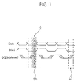
- the three superimposed diagrams indicate the data signal (Data), the DQS signal (DQS), as well as the delayed DQS signal (DQS_delayed).
- the reference SM designates the safety-time margin, whilst the reference AJ designates the added jitter. It will be appreciated that the safety margin SM has been indicated as referring to an amplitude Q corresponding to a quarter of the period of the signals considered.
- the range of possible variation in the clock frequency of normal DDR-SDRAM memories may be somewhat wide (e.g., 50-200 MHz): the maximum tolerable amount of jitter must therefore be considered not so much in absolute terms as rather in relation to the frequency (and hence to the period) of operation of the memory, which is a quantity that is subject to variation.
- US-A-6087868 describes a digital delay-locked loop (DLL) comprising a digital delay line having associated to it a digital phase detector that is able to control the propagation delay of the delay line so as to obtain the synchronization between the internal clock and a reference clock.
- the DLL loop is open until the internal clock signal and a reference clock-signal edge come to be simultaneously in the phase-detection region.
- the variable delay is increased starting from a minimum value until the edge of the phase-detection region exceeds the edge considered as reference.
- a clock-jitter filter is enabled in order to obtain a rejection effect on the jitter associated to the reference clock.
- the purpose of the present invention is therefore to meet the requirements referred to above in an altogether satisfactory way.
- the invention also relates to a storage element (DDR-SDRAM) which incorporates said delay line.
- DDR-SDRAM storage element
- the solution according to the invention envisages providing a programmable delay line with an added control of the resolution time, with the aim of keeping the jitter proportional to the period of the input signal.
- the delay line can be used in a DLL, with the advantage provided by the fact that the resolution (i.e., the jitter) follows the trace of the period of the input signal. Given that the frequency rate of the DLL at which the system operates depends upon the resolution, a wider working frequency is obtained by keeping a satisfactory time margin.
- the solution according to the invention enables, in particular, implementation of a DLL capable of working in a wide range of frequencies (50-200 MHz), which may be used for the majority of DDR-SDRAM storage devices available on the market.
- Both the diagram of Figure 2 and the diagram of Figure 3 illustrate the structure of a delay line 1 (in Figure 2) and 1' (in Figure 3) designed to perform its function on an input signal IS so as to generate an output signal OS delayed by a pre-determined time interval.
- the input signal IS is constituted by the DQS signal
- the output signal OS is constituted by the delayed DQS signal DQS_delayed.
- the invention stems from the observation that the safety margin for the data set-up and the hold time at the synchronization flip-flop depends upon the difference between the value of one quarter of period QP of the DQS signal and the added jitter AJ added in the delayed DQS signal.
- the safety margin is reduced as the period of the DQS signal is reduced.
- the solution according to the invention consequently envisages implementation of a programmable delay line with a function of additional control so as to be able to adjust the time resolution (and hence the jitter) and keep the latter proportional to the period of the DQS signal.
- the main advantage of this implementation is provided by the fact that (with reference to the application to a DDR-SDRAM) the resolution can follow the period of the DQS signal. Given that the range of frequencies of operation of the DLL depends upon the resolution, it is possible to obtain a wider range of frequencies of operation, at the same time maintaining a reasonable safety margin.
- the solution according to the invention is, by its intrinsic nature, of a modular type.
- This solution enables, in fact, generation, starting from individual delay modules d (which retard the signal brought to their inputs by an amount equal to the value d), of a maximum delay value.
- this maximum delay corresponds to 2d (with a resolution factor ⁇ r, where r denotes the resolution or jitter).
- the delay in question is respectively equal to 2d or 4d with a resolution margin that continues to be ⁇ r, and hence, virtually, with a doubling of the delay that does not increase the jitter.
- the jitter varies as the delay time varies.
- the solution according to the invention envisages, more precisely, making the jitter vary proportionally to the clock period.
- the solution according to the invention ensures that, for short clock periods (high operating frequencies) a low jitter is obtained, and for longer clock periods (low operating frequencies) a proportionally higher jitter is obtained.
- the jitter depends, in fact, upon the power supply noise and upon the thermal gradients that are largely invariant with respect to the delay time, as well as upon the resolution of the individual delay module, all these being factors that depend exclusively upon the module itself.
- the architecture of the delay module is designed in such a way as to give rise to a jitter that adapts to the frequency of the system in such a way as to maintain the period/jitter ratio constant.
- the values assumed by the signal delay_sel enable selective activation of one or both of the delay elements d.
- this can be done according to a signal T which indicates the value of the period (and hence of the frequency) of operation of the memory supplied to the control logic LC.
- each unit 10 comprises an input line 101, which is doubled on a first branch 1010, which functions as input for a delay module d, and on another branch designated by 1011, which goes to a first input of a delay module d' of a combinatorial type (it may, for instance, simply be a flip-flop), provided with another input to which the signal at output from the delay module d referred to previously is brought.
- a combinatorial type it may, for instance, simply be a flip-flop
- Each module d' is configured in such a way that, if the signal resolution_sel has a logic value 0, the element d' behaves simply like a delay line (with a delay value which will here be assumed simply as being equal to d even though at least in principle the value could be other than d).
- the delay line 1' behaves (according to the value assumed by the signal delay_sel) in the same way as the delay line 1 described previously with reference to Figure 2.
- each one of the units 10 behaves in practice as the cascading of two delay modules with a total delay value equal to 2d (it is, in fact - in the framework of each element 10 - the delay deriving from the sum of the delay imparted by the module d to the signal brought onto the line 1010 and of the additional delay - also this assumed as being equal to d - applied to the same signal by the element d').
- the total delay value can be brought up to a value equal to 4d, maintaining, however, the resolution value ⁇ r, this in so far as the main sources of jitter (the noise present on the power supply and the temperature gradients) affect the circuit in the same way irrespective of the delay value attained.
Landscapes
- Engineering & Computer Science (AREA)
- Microelectronics & Electronic Packaging (AREA)
- Computer Hardware Design (AREA)
- Physics & Mathematics (AREA)
- Nonlinear Science (AREA)
- Dram (AREA)
- Pulse Circuits (AREA)
Abstract
A programmable delay element comprises a plurality
of delay modules (d, d'), which can be connected
together for generating, starting from an input signal
(IS), an output signal (OS) delayed with a pre-determined
time-delay value referred to a given value
(T) of operating period. A control logic (LC)
selectively connects together the-delay modules (d, d')
in such a way as to obtain the aforesaid pre-determined
time-delay value. The arrangement is such that the
jitter present on the delayed output signal (OS) is
made to vary proportionally to the operating period (T)
so as to maintain the ratio between said period (T) and
said jitter substantially constant. The element is
usable in particular in memories of the DDR-SDRAM type
for generating the delayed DQS signal (DQS_delayed)
with the possibility of varying selectively the amount
of delay as a function of the frequency (T) of
operation of the memory.
Description
The present invention relates to delay lines and
has been developed with particular attention paid to
their possible application in the field of memories, in
particular in SDRAM memories with double data rate
(DDR).
In normal SDRAM memories of the DDR type, the data
and the data quadrature strobe (DQS) signal are emitted
by the memory in a synchronous way and in phase with
one another on the rising and falling edges.
In order to obtain an exact set-up of the data and
a correct hold time at the flip-flop functioning as
latch, the DQS signal must be delayed.
In particular, with a 90° delay (i.e., one quarter
of the period of the signals considered) and with an
accurate delay of the DQS signal at the rising and
falling edges, it is possible, according to the
frequency range of the DQS and the performance of the
flip-flop, to obtain an ample margin of tolerance both
for the set-up of the data and for the hold time.
However, when the DQS signal is delayed by getting
it to pass through a delay line, the delay value is
inevitably affected by a certain margin of jitter as a
result of the noise present on the power-supply lines,
of the temperature gradients, etc.
In the timing diagram of Figure 1, the three
superimposed diagrams indicate the data signal (Data),
the DQS signal (DQS), as well as the delayed DQS signal
(DQS_delayed).
The reference SM designates the safety-time margin,
whilst the reference AJ designates the added jitter. It
will be appreciated that the safety margin SM has been
indicated as referring to an amplitude Q corresponding
to a quarter of the period of the signals considered.
In this context, there exists the problem of
keeping the jitter as low as possible so as to ensure a
time margin sufficient for the set-up and the hold time
at the synchronization flip-flop.
The range of possible variation in the clock
frequency of normal DDR-SDRAM memories may be somewhat
wide (e.g., 50-200 MHz): the maximum tolerable amount
of jitter must therefore be considered not so much in
absolute terms as rather in relation to the frequency
(and hence to the period) of operation of the memory,
which is a quantity that is subject to variation.
The above requirement does not appear so far to
have encountered an adequate response at a technical
level, as emerges, for instance, from US-A-6087868,
US-A-6125157, and US-A-6140854, as well as from the
publication "A Register Controlled Symmetrical DLL for
Double Data Rate DRAM", IEEE Journal of Solid State
Circuits, Vol. 34, No. 4, April 1999.
For example, US-A-6087868 describes a digital
delay-locked loop (DLL) comprising a digital delay line
having associated to it a digital phase detector that
is able to control the propagation delay of the delay
line so as to obtain the synchronization between the
internal clock and a reference clock. The DLL loop is
open until the internal clock signal and a reference
clock-signal edge come to be simultaneously in the
phase-detection region. To obtain the locking condition
of the DLL, the variable delay is increased starting
from a minimum value until the edge of the phase-detection
region exceeds the edge considered as
reference. Once the DLL loop is closed, a clock-jitter
filter is enabled in order to obtain a rejection effect
on the jitter associated to the reference clock.
The solution described in US-A-6125157, instead,
envisages the use of a chain of delay elements, which
receives at input a clock signal. At output from the
delay elements there is thus generated a set of phase
vectors. The delays of these elements are regulated by
a first DLL, whilst a second DLL chooses a pair of
phase vectors that embraces the phase of an input
clock. By means of a phase interpolator, an output
clock signal is then generated, as well as a delayed
version of the latter. A phase detector compares the
delayed clock signal at output with the clock signal at
input and adjusts the phase interpolator so that the
delayed clock present at output is in phase with the
clock at input.
Finally, the solution described in US-A-6140854
envisages the use of a DLL comprising a delay line, the
delay of which can be varied by means of a counter that
is incremented to vary the delay. A so-called shifting-delay
circuit is present, which operates on the basis
of half-periods of a reference clock linked to the
source clock. The total delay of the source clock
derives from a combination of the action of delay of
the aforesaid circuit and of the delay line, the latter
occupying areas of silicon that are relatively
extensive.
Apart from any other consideration, the above-mentioned
solutions prove somewhat complex and
burdensome to implement.
The purpose of the present invention is therefore
to meet the requirements referred to above in an
altogether satisfactory way.
According to the present invention, the above
purpose is achieved thanks to a programmable delay line
having the characteristics referred to in the ensuing
claims. The invention also relates to a storage element
(DDR-SDRAM) which incorporates said delay line.
Basically, the solution according to the invention
envisages providing a programmable delay line with an
added control of the resolution time, with the aim of
keeping the jitter proportional to the period of the
input signal.
The delay line can be used in a DLL, with the
advantage provided by the fact that the resolution
(i.e., the jitter) follows the trace of the period of
the input signal. Given that the frequency rate of the
DLL at which the system operates depends upon the
resolution, a wider working frequency is obtained by
keeping a satisfactory time margin.
The solution according to the invention enables, in
particular, implementation of a DLL capable of working
in a wide range of frequencies (50-200 MHz), which may
be used for the majority of DDR-SDRAM storage devices
available on the market.
The present invention will now be described, purely
by way of non-limiting example, with reference to the
attached drawings, in which:
- Figure 1, which is aimed at enabling definition of the problem underlying the present invention, has already been described previously; and
- Figures 2 and 3 illustrate, in the form of circuit block diagrams, two possible different embodiments of the solution according to the invention.
Both the diagram of Figure 2 and the diagram of
Figure 3 illustrate the structure of a delay line 1 (in
Figure 2) and 1' (in Figure 3) designed to perform its
function on an input signal IS so as to generate an
output signal OS delayed by a pre-determined time
interval.
With specific reference to the preferred (but not
imperative) application to which reference has been
made in the introductory part of this description, the
input signal IS is constituted by the DQS signal,
whilst the output signal OS is constituted by the
delayed DQS signal DQS_delayed.
With a view to the said application, the invention
stems from the observation that the safety margin for
the data set-up and the hold time at the
synchronization flip-flop depends upon the difference
between the value of one quarter of period QP of the
DQS signal and the added jitter AJ added in the delayed
DQS signal.
Consequently, for a fixed jitter value, the safety
margin is reduced as the period of the DQS signal is
reduced.
In order to maintain the safety margin within a
desired range as the period of the DQS signal varies,
it is possible to control the jitter in view of the
fact that the latter depends, proportionally, upon the
resolution of the delay line.
The solution according to the invention
consequently envisages implementation of a programmable
delay line with a function of additional control so as
to be able to adjust the time resolution (and hence the
jitter) and keep the latter proportional to the period
of the DQS signal.
The main advantage of this implementation is
provided by the fact that (with reference to the
application to a DDR-SDRAM) the resolution can follow
the period of the DQS signal. Given that the range of
frequencies of operation of the DLL depends upon the
resolution, it is possible to obtain a wider range of
frequencies of operation, at the same time maintaining
a reasonable safety margin.
In both of the solutions illustrated in Figures 2
and 3, the use is envisaged, in the framework of a DLL,
of a delay line 1, 1', respectively, subjected to a
control logic LC capable of generating:
- a first logic signal called delay_sel, and
- in the case of the embodiment of Figure 3, a second logic signal called resolution_sel.
From the ensuing more detailed illustration it will
be appreciated that the solution according to the
invention is, by its intrinsic nature, of a modular
type. This solution enables, in fact, generation,
starting from individual delay modules d (which retard
the signal brought to their inputs by an amount equal
to the value d), of a maximum delay value. In the case
of the embodiment of Figure 2, this maximum delay
corresponds to 2d (with a resolution factor ±r, where r
denotes the resolution or jitter). In the case of the
embodiment illustrated in Figure 3, the delay in
question is respectively equal to 2d or 4d with a
resolution margin that continues to be ±r, and hence,
virtually, with a doubling of the delay that does not
increase the jitter.
In actual fact, the jitter varies as the delay time
varies. The solution according to the invention
envisages, more precisely, making the jitter vary
proportionally to the clock period.
The solution according to the invention ensures
that, for short clock periods (high operating
frequencies) a low jitter is obtained, and for longer
clock periods (low operating frequencies) a
proportionally higher jitter is obtained.
The jitter depends, in fact, upon the power supply
noise and upon the thermal gradients that are largely
invariant with respect to the delay time, as well as
upon the resolution of the individual delay module, all
these being factors that depend exclusively upon the
module itself.
The architecture of the delay module is designed in
such a way as to give rise to a jitter that adapts to
the frequency of the system in such a way as to
maintain the period/jitter ratio constant.
It is, on the other hand, evident that the same
principle illustrated here can be extended to even
greater delay values than the values 2d and 4d, here
cited purely by way of example. This result can be
obtained, for instance, using a larger number of
individual delay elements d and modifying accordingly
the control logic LC, so as to give rise to output
signals that express more complex logical combinations.
In the case of the delay line 1 of Figure 2, the
values assumed by the signal delay_sel enable selective
activation of one or both of the delay elements d.
In particular, in the case of the proposed
application to a DDR-SDRAM memory, this can be done
according to a signal T which indicates the value of
the period (and hence of the frequency) of operation of
the memory supplied to the control logic LC.
To a halving of the operating period there can thus
correspond a halving of the total delay value imparted
to the signal IS.
This flexibility of operation is further developed
in the case of the embodiment of Figure 3, where the
delay line 1' is constituted by the cascading of two
homologous delay units, designated by 10. Each unit 10
comprises an input line 101, which is doubled on a
first branch 1010, which functions as input for a delay
module d, and on another branch designated by 1011,
which goes to a first input of a delay module d' of a
combinatorial type (it may, for instance, simply be a
flip-flop), provided with another input to which the
signal at output from the delay module d referred to
previously is brought.
Each module d' is configured in such a way that, if
the signal resolution_sel has a logic value 0, the
element d' behaves simply like a delay line (with a
delay value which will here be assumed simply as being
equal to d even though at least in principle the value
could be other than d).
In this case, the delay line 1' behaves (according
to the value assumed by the signal delay_sel) in the
same way as the delay line 1 described previously with
reference to Figure 2.
If, instead, the signal resolution_sel assumes the
logic value 1, then each one of the units 10 behaves in
practice as the cascading of two delay modules with a
total delay value equal to 2d (it is, in fact - in the
framework of each element 10 - the delay deriving from
the sum of the delay imparted by the module d to the
signal brought onto the line 1010 and of the additional
delay - also this assumed as being equal to d - applied
to the same signal by the element d').
As has already been said, in this case the total
delay value can be brought up to a value equal to 4d,
maintaining, however, the resolution value ±r, this in
so far as the main sources of jitter (the noise present
on the power supply and the temperature gradients)
affect the circuit in the same way irrespective of the
delay value attained.
Of course, without prejudice to the principle of
the invention, the details of construction and the
embodiments may vary widely with respect to what is
described and illustrated herein, without thereby
departing from the scope of the present invention as
defined in the ensuing claims.
Claims (6)
- A programmable delay element, characterized in that it comprises:a plurality of delay modules (d, d'), which can be connected together for generating, starting from an input signal (IS), an output signal (OS) delayed with a pre-determined time-delay value referred to a given value (T) of operating period; said delayed output signal being affected by jitter (AJ); anda control logic (LC) for selectively connecting together the delay modules (d, d') of said plurality in such a way as to obtain said value of pre-determined time delay referred to a given value (T) of operating period as a result of connection of said modules (d, d'); the arrangement being such as to cause said jitter to vary proportionally to said operating period (T) so as to maintain the ratio between said period (T) sand said jitter substantially constant.
- The element according to Claim 1, characterized in that said control logic (LC) generates at least one first control signal (delay_sel) to identify selectively the delay modules (d, d') of said plurality that are activated.
- The element according to Claim 2, characterized in that said delay modules are arranged in a plurality of pairs (d, d'), and in that said control logic (LC) is able to generate also a second logic signal (resolution_sel) for determining, within each pair of said delay modules (d, d') activated as a result of emission of said at least one first logic signal (delay_sel), selective activation of one or of both of the delay modules (d, d') comprises in the pair.
- The element according to Claim 3, characterized in that in said pair, one (d') of the delay elements carries, associated thereto, a combinatorial function driven by said second logic signal (resolution_sel).
- A memory, such as a memory of the DDR-SDRAM type, provided with a function for generating a delayed DQS signal (DQS_delayed), characterized in that it comprises a delay element according to any one of Claims 1 to 4 for generating a version (DQS_delayed) of said DQS signal delayed by a pre-determined amount of time, and in that said delay element is configured in such a way that said pre-determined amount of time is varied with reference to said given value (T) of operating period, the latter given value being identified by the frequency of operation of the memory.
- The memory according to Claim 5, characterized in that said predetermined amount of time is substantially equal to one quarter (90°) of said given value (T) of operating period.
Priority Applications (2)
| Application Number | Priority Date | Filing Date | Title |
|---|---|---|---|
| EP01830368A EP1265247A1 (en) | 2001-06-05 | 2001-06-05 | A programmable delay line and corresponding memory |
| US10/164,323 US20030001651A1 (en) | 2001-06-05 | 2002-06-05 | Programmable delay line and corresponding memory |
Applications Claiming Priority (1)
| Application Number | Priority Date | Filing Date | Title |
|---|---|---|---|
| EP01830368A EP1265247A1 (en) | 2001-06-05 | 2001-06-05 | A programmable delay line and corresponding memory |
Publications (1)
| Publication Number | Publication Date |
|---|---|
| EP1265247A1 true EP1265247A1 (en) | 2002-12-11 |
Family
ID=8184555
Family Applications (1)
| Application Number | Title | Priority Date | Filing Date |
|---|---|---|---|
| EP01830368A Withdrawn EP1265247A1 (en) | 2001-06-05 | 2001-06-05 | A programmable delay line and corresponding memory |
Country Status (2)
| Country | Link |
|---|---|
| US (1) | US20030001651A1 (en) |
| EP (1) | EP1265247A1 (en) |
Cited By (3)
| Publication number | Priority date | Publication date | Assignee | Title |
|---|---|---|---|---|
| WO2007040859A1 (en) * | 2005-09-30 | 2007-04-12 | Advanced Micro Devices, Inc. | Voltage controlled delay line (vcdl) having embedded multiplexer and interpolation functions |
| US7256636B2 (en) | 2005-09-16 | 2007-08-14 | Advanced Micro Devices, Inc. | Voltage controlled delay line (VCDL) having embedded multiplexer and interpolation functions |
| CN113377049A (en) * | 2021-06-11 | 2021-09-10 | 西安应用光学研究所 | DDR control method based on FPGA low-delay video image cache |
Families Citing this family (9)
| Publication number | Priority date | Publication date | Assignee | Title |
|---|---|---|---|---|
| US7117382B2 (en) * | 2002-05-30 | 2006-10-03 | Sun Microsystems, Inc. | Variably controlled delay line for read data capture timing window |
| US20040225976A1 (en) * | 2002-05-30 | 2004-11-11 | Cheung Daniel Y. | Glitch free programmable delay line for edge sensitive design |
| US6891774B1 (en) * | 2003-09-03 | 2005-05-10 | T-Ram, Inc. | Delay line and output clock generator using same |
| US7464282B1 (en) | 2003-09-03 | 2008-12-09 | T-Ram Semiconductor, Inc. | Apparatus and method for producing dummy data and output clock generator using same |
| US7882322B2 (en) * | 2006-06-27 | 2011-02-01 | International Business Machines Corporation | Early directory access of a double data rate elastic interface |
| US7752475B2 (en) * | 2006-06-27 | 2010-07-06 | International Business Machines Corporation | Late data launch for a double data rate elastic interface |
| US7739538B2 (en) * | 2006-06-27 | 2010-06-15 | International Business Machines Corporation | Double data rate chaining for synchronous DDR interfaces |
| US7734944B2 (en) * | 2006-06-27 | 2010-06-08 | International Business Machines Corporation | Mechanism for windaging of a double rate driver |
| US7783911B2 (en) * | 2006-06-27 | 2010-08-24 | International Business Machines Corporation | Programmable bus driver launch delay/cycle delay to reduce elastic interface elasticity requirements |
Citations (3)
| Publication number | Priority date | Publication date | Assignee | Title |
|---|---|---|---|---|
| US5646564A (en) * | 1994-09-02 | 1997-07-08 | Xilinx, Inc. | Phase-locked delay loop for clock correction |
| US6125157A (en) * | 1997-02-06 | 2000-09-26 | Rambus, Inc. | Delay-locked loop circuitry for clock delay adjustment |
| US6147532A (en) * | 1998-08-07 | 2000-11-14 | Mitsubishi Denki Kabushiki Kaisha | PLL circuit capable of preventing malfunction of FF circuits connected thereto and semiconductor integrated circuit including the PLL circuit |
-
2001
- 2001-06-05 EP EP01830368A patent/EP1265247A1/en not_active Withdrawn
-
2002
- 2002-06-05 US US10/164,323 patent/US20030001651A1/en not_active Abandoned
Patent Citations (3)
| Publication number | Priority date | Publication date | Assignee | Title |
|---|---|---|---|---|
| US5646564A (en) * | 1994-09-02 | 1997-07-08 | Xilinx, Inc. | Phase-locked delay loop for clock correction |
| US6125157A (en) * | 1997-02-06 | 2000-09-26 | Rambus, Inc. | Delay-locked loop circuitry for clock delay adjustment |
| US6147532A (en) * | 1998-08-07 | 2000-11-14 | Mitsubishi Denki Kabushiki Kaisha | PLL circuit capable of preventing malfunction of FF circuits connected thereto and semiconductor integrated circuit including the PLL circuit |
Non-Patent Citations (2)
| Title |
|---|
| EFENDOVICH ET AL: "Multi-frequency zero-jitter delay-locked loop", CUSTOM INTEGRATED CIRCUITS CONFERENCE, 1993., PROCEEDINGS OF THE IEEE 1993 SAN DIEGO, CA, USA 9-12 MAY 1993, NEW YORK, NY, USA,IEEE, 9 May 1993 (1993-05-09), pages 2711 - 2714, XP010222179, ISBN: 0-7803-0826-3 * |
| LIN F ET AL: "A REGISTER-CONTROLLED SYMMETRICAL DLL FOR DOUBLE-DATA-RATE DRAM", IEEE JOURNAL OF SOLID-STATE CIRCUITS, IEEE INC. NEW YORK, US, vol. 34, no. 4, April 1999 (1999-04-01), pages 565 - 568, XP000893670, ISSN: 0018-9200 * |
Cited By (3)
| Publication number | Priority date | Publication date | Assignee | Title |
|---|---|---|---|---|
| US7256636B2 (en) | 2005-09-16 | 2007-08-14 | Advanced Micro Devices, Inc. | Voltage controlled delay line (VCDL) having embedded multiplexer and interpolation functions |
| WO2007040859A1 (en) * | 2005-09-30 | 2007-04-12 | Advanced Micro Devices, Inc. | Voltage controlled delay line (vcdl) having embedded multiplexer and interpolation functions |
| CN113377049A (en) * | 2021-06-11 | 2021-09-10 | 西安应用光学研究所 | DDR control method based on FPGA low-delay video image cache |
Also Published As
| Publication number | Publication date |
|---|---|
| US20030001651A1 (en) | 2003-01-02 |
Similar Documents
| Publication | Publication Date | Title |
|---|---|---|
| KR100624871B1 (en) | Clock latency compensation circuit for ddr timing | |
| US10700689B2 (en) | Apparatuses and methods for detecting a loop count in a delay-locked loop | |
| KR100554981B1 (en) | Delay lock loop | |
| US6424198B1 (en) | Memory clock generation with configurable phase advance and delay capability | |
| CN100574110C (en) | Synchronization circuit and synchronization method | |
| US8536914B2 (en) | DLL including 2-phase delay line and duty correction circuit and duty correction method thereof | |
| US7368966B2 (en) | Clock generator and clock duty cycle correction method | |
| US20050083099A1 (en) | Capture clock generator using master and slave delay locked loops | |
| US20190363724A1 (en) | Dll circuit having variable clock divider | |
| US6815985B2 (en) | Clock divider and method for dividing a clock signal in a DLL circuit | |
| US8698533B2 (en) | Phase mixer with adjustable load-to-drive ratio | |
| JP4944373B2 (en) | Delay locked loop circuit | |
| KR20070045276A (en) | Method and apparatus for setting tuning range for analog delay | |
| US20030001651A1 (en) | Programmable delay line and corresponding memory | |
| US20040099883A1 (en) | Delay locked loop (DLL) in semiconductor device | |
| US8134391B2 (en) | Semiconductor devices with signal synchronization circuits | |
| KR100400041B1 (en) | Method and DLL(Delay Locked Loop) with controlling phase precisely | |
| US7605624B2 (en) | Delay locked loop (DLL) circuit for generating clock signal for memory device | |
| US8264267B2 (en) | Clock pulse generating circuit | |
| CN116192127A (en) | A Single Delay Line High Frequency Phase Locked Loop and Its Memory | |
| KR20040023838A (en) | Register controlled delay locked loop | |
| KR100808592B1 (en) | Delay lock loop circuit | |
| KR100915808B1 (en) | Delay Circuit and Delay Method of Delay Fixed Loop Circuit | |
| KR101002925B1 (en) | Delay fixed loop circuit | |
| KR100608382B1 (en) | Output Enable Signal Generation Circuit |
Legal Events
| Date | Code | Title | Description |
|---|---|---|---|
| PUAI | Public reference made under article 153(3) epc to a published international application that has entered the european phase |
Free format text: ORIGINAL CODE: 0009012 |
|
| AK | Designated contracting states |
Kind code of ref document: A1 Designated state(s): AT BE CH CY DE DK ES FI FR GB GR IE IT LI LU MC NL PT SE TR |
|
| AX | Request for extension of the european patent |
Free format text: AL;LT;LV;MK;RO;SI |
|
| 17P | Request for examination filed |
Effective date: 20030210 |
|
| AKX | Designation fees paid |
Designated state(s): DE FR GB IT |
|
| 17Q | First examination report despatched |
Effective date: 20070625 |
|
| STAA | Information on the status of an ep patent application or granted ep patent |
Free format text: STATUS: THE APPLICATION HAS BEEN WITHDRAWN |
|
| 18W | Application withdrawn |
Effective date: 20071108 |