EP1265087A2 - Optical module, method of aligning an optical module and device for aligning an optical module - Google Patents
Optical module, method of aligning an optical module and device for aligning an optical module Download PDFInfo
- Publication number
- EP1265087A2 EP1265087A2 EP02254025A EP02254025A EP1265087A2 EP 1265087 A2 EP1265087 A2 EP 1265087A2 EP 02254025 A EP02254025 A EP 02254025A EP 02254025 A EP02254025 A EP 02254025A EP 1265087 A2 EP1265087 A2 EP 1265087A2
- Authority
- EP
- European Patent Office
- Prior art keywords
- optical
- light
- aligning
- interference patterns
- object light
- Prior art date
- Legal status (The legal status is an assumption and is not a legal conclusion. Google has not performed a legal analysis and makes no representation as to the accuracy of the status listed.)
- Withdrawn
Links
Images




Classifications
-
- G—PHYSICS
- G02—OPTICS
- G02B—OPTICAL ELEMENTS, SYSTEMS OR APPARATUS
- G02B6/00—Light guides; Structural details of arrangements comprising light guides and other optical elements, e.g. couplings
- G02B6/24—Coupling light guides
- G02B6/26—Optical coupling means
- G02B6/32—Optical coupling means having lens focusing means positioned between opposed fibre ends
-
- G—PHYSICS
- G02—OPTICS
- G02B—OPTICAL ELEMENTS, SYSTEMS OR APPARATUS
- G02B6/00—Light guides; Structural details of arrangements comprising light guides and other optical elements, e.g. couplings
- G02B6/24—Coupling light guides
- G02B6/36—Mechanical coupling means
- G02B6/3628—Mechanical coupling means for mounting fibres to supporting carriers
- G02B6/3664—2D cross sectional arrangements of the fibres
- G02B6/3672—2D cross sectional arrangements of the fibres with fibres arranged in a regular matrix array
-
- G—PHYSICS
- G02—OPTICS
- G02B—OPTICAL ELEMENTS, SYSTEMS OR APPARATUS
- G02B6/00—Light guides; Structural details of arrangements comprising light guides and other optical elements, e.g. couplings
- G02B6/24—Coupling light guides
- G02B6/42—Coupling light guides with opto-electronic elements
- G02B6/4201—Packages, e.g. shape, construction, internal or external details
- G02B6/4219—Mechanical fixtures for holding or positioning the elements relative to each other in the couplings; Alignment methods for the elements, e.g. measuring or observing methods especially used therefor
- G02B6/422—Active alignment, i.e. moving the elements in response to the detected degree of coupling or position of the elements
- G02B6/4227—Active alignment methods, e.g. procedures and algorithms
-
- G—PHYSICS
- G02—OPTICS
- G02B—OPTICAL ELEMENTS, SYSTEMS OR APPARATUS
- G02B6/00—Light guides; Structural details of arrangements comprising light guides and other optical elements, e.g. couplings
- G02B6/24—Coupling light guides
- G02B6/42—Coupling light guides with opto-electronic elements
- G02B6/4201—Packages, e.g. shape, construction, internal or external details
- G02B6/4219—Mechanical fixtures for holding or positioning the elements relative to each other in the couplings; Alignment methods for the elements, e.g. measuring or observing methods especially used therefor
- G02B6/422—Active alignment, i.e. moving the elements in response to the detected degree of coupling or position of the elements
- G02B6/4225—Active alignment, i.e. moving the elements in response to the detected degree of coupling or position of the elements by a direct measurement of the degree of coupling, e.g. the amount of light power coupled to the fibre or the opto-electronic element
Definitions
- the present invention relates to an alignment method for aligning optical axes of an optical fiber array and a microlens array which form an optical module, the optical module aligned by the alignment method, and a device for performing the alignment method.
- An optical module for optical communication which coupled an optical fiber array to a microlens array is known.
- This module is provided to cause light from a light emitting diode to enter the microlens through an optical fiber and to take it out as collimated light or to cause the collimated light to enter the optical fiber through the microlens.
- optical module it is essential for the optical axes of the optical fiber and the microlens to agree with each other for improvement of communication accuracy.
- An optical axis adjustment method for this optical module is disclosed in Japanese Unexamined Patent Publication No. Hei 9-061666.
- a mask having a mesh-shaped pattern of the same array pitch as that of an optical fiber array and a collimation lens array i.e., microlens array
- a detector which detects light beam shape.
- Light is caused to enter the collimation lens array through the optical fiber array, and the light emitted from the collimation lens array and passed without being blocked off by the mask is sensed by the detector.
- a relative position of the optical fiber array and the collimation lens array is adjusted so that the light beam shape corresponding to each optical fiber can be uniform.
- an alignment method of an optical module in which alignment of the optical module comprising an optical fiber array in which a plurality of optical fibers are disposed in one or two-dimensional manner and a microlens array in which a plurality of microlenses are disposed in one or two-dimensional manner is made, characterized in that a laser beam emitted from a laser beam source is split into object light and reference light and the object light is caused to enter at least one of the plurality of optical fibers and to emit from the microlens array, wherein the reference light is provided to overlap the emitted object light so as to generate interference patterns, thereby making fine adjustments to relative position of the optical fiber array and the microlens array based on the interference patterns.
- An alignment device of the optical module according to the present invention comprises a means for splitting a laser beam from a laser beam source into object light and reference light, a means for guiding the object light to an optical fiber, a light coupling means for overlapping the object light emitted from a microlens array and the reference light with each other to generate interference patterns, light observation means for observing the interference patterns, and a means for making fine adjustments to the relative position of an optical fiber array and the microlens array based on the interference patterns.
- the interference patterns of the object light and the reference light greatly change even by a slight shift or deviation of the optical axis. Accordingly, it is possible to precisely make fine adjustments to the optical axis using these interference patterns.
- An efficient alignment method is provided in which the object light is caused to enter two optical fibers and to overlap reference light so as to generate two interference patterns, wherein fine adjustments are made to the relative position of the optical fiber array and microlens array to allow the two interference patterns to approximate.
- the two interference patterns be the same as each other, but they don't have to be completely the same.
- the object light split by a light splitter is caused to enter the two optical fibers forming the optical fiber array through a coupling member.
- wave front phase analysis software is installed within a control device such as a personal computer, wherein the wave front phase is analyzed from the interference fringes of the two interference patterns to allow these wave front phases to approximate.
- a phase of the object light or reference light can be shifted.
- a phase shifting means is provided in the optical path of the reference light or the optical path of the object light emitted from the microlens array.
- the interference patterns on the position spaced away by a predetermined distance from the microlens array are used.
- the laser beam is a Gausian beam provided with a beam waist.
- the wave front phase becomes a plane wave.
- the light observation means shall be provided with an image input element such as a CCD camera or a camera tube, and an optical system for forming an image in a position spaced apart a predetermined distance from the microlens on the image input element.
- an image input element such as a CCD camera or a camera tube
- an optical system for forming an image in a position spaced apart a predetermined distance from the microlens on the image input element.
- the target optical module can be obtained by bonding the optical fiber array and the microlens array together in such a condition.
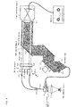
- Fig. 1 is a schematic diagram of a device for use in an alignment method of the present invention.
- Reference numeral 1 is a semiconductor laser serving as a light-emitting source
- 2 is a light-splitting means for splitting a laser beam from the semiconductor laser into object light and reference light
- 3 is an optical module.
- 4 is a light coupling means for overlapping the object light transmitted through the optical module and the reference light with each other
- 5 is a light observation means for observing an interference pattern caused by overlapping the object light and the reference light with each other.
- the light-splitting means 2 is provided with a coupling lens 21 and a beam splitter 22.
- a laser beam is split into object light and reference light by the beam splitter 22.
- the object light is connected to two optical fibers of an optical fiber array 31 forming the optical module 3 through a single mode optical fiber 23, a light-branching section 24, and a coupling 25.
- the reference light is fed to the light coupling means 4 through a single mode optical fiber 26.
- Fig. 2 (a) is a side view showing one example of an optical module and Fig. 2 (b) is a view taken in the direction of the arrow A of Fig. 1 (a) showing an optical fiber.
- the optical module 3 is composed of the optical fiber array 31 and a microlens array 32.
- the optical fiber array 31 and the microlens array 32 are firmly secured to the optical module 3 after it is completed as a finished product.
- one of them i.e. the optical fiber array 31
- the optical fiber array 31 is slightly movable in the direction of the X, Y, and Z axes and rotatable around each axis by a known means because adjustment of the optical axis is conducted in the present invention.
- the optical fiber array 31 has a silicon substrate 33 provided with V-grooves at regular intervals in one or two-dimensional shape, and single mode optical fibers 34 are secured in the grooves.
- the optical fiber array 31 is not necessarily limited to this construction, but it may be formed in such a manner that a stainless steel substrate or glass substrate is formed with openings in advance into which the optical fibers are inserted and secured.
- the microlens array 32 has a glass substrate 35 provided with a plurality of microlenses 36 corresponding to the optical fibers 34.
- the microlens 36 can be formed by 2P molding method using ultraviolet ray-setting resin, a method whereby an etching is effected on a glass substrate surface through a mask to form many recessions into which resin of high refractive index is filled, a method whereby ions are diffused on a glass substrate surface through a mask to change a refractive index, etc.
- the light coupling means 4 is provided with a collimator lens 41 and a half lens 42. After reference light is changed to parallel light by the collimator lens 41, the parallel light is folded back by the half mirror 42 in the same direction as object light emitted from the microlens array 32 to overlap the object light, thereby generating an interference pattern.
- the light observation means 5 is composed of a CCD camera or a camera tube provided with an image formation lens 51 and a photodetector element 52.
- the interference pattern on an observation surface on the downstream side of the light coupling means 4 is formed on the photodetector 52 and displayed on a monitor 53.
- Figs. 3 (a) and (b) are views showing wave fronts of the object light.
- Fig. 3 (a) shows the case where an optical axis of the optical fiber 34 agrees with that of the microlens 36 while
- Fig. 3 (b) shows the case where the optical axis of the optical fiber 34 does not agree with that of the microlens 36.
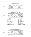
- Figs. 4 (a) through (c) are views showing the overlapping conditions of the object light and the reference light, and the interference patterns caused by such conditions.
- the wave front of the object light becomes parallel to that of the reference light as shown in Fig. 4 (a).
- the interference fringe i.e., interference pattern
- the object light is a plane wave, but not parallel to the wave front of the reference light as shown in Fig. 4 (b). In this case, linear interference fringes are generated.
- the interference fringes show equiphase line (i.e., contour line) of the wave front of the object light generated by causing the object light to interfere with the reference light.
- equiphase line i.e., contour line
- the spherical wave is generated because the observation surface is situated off the beam waist. Accordingly, as shown by the arrow in Fig. 3 (c), the interference fringes can be removed by relatively moving the optical fiber array in the direction of the optical axis.
- the object light is caused to enter two optical fibers, as shown in Fig. 5 (a) or (b), two interference patters P1 and P2 are displayed on a monitor.
- the optical axes of the optical fiber and microlens corresponding to the interference pattern P1 shift in the direction of X - X while no shift is produced between the optical axes of the optical fiber and microlens.
- the example shown in Fig. 5 (a) the optical axes of the optical fiber and microlens corresponding to the interference pattern P1 shift in the direction of X - X while no shift is produced between the optical axes of the optical fiber and microlens.
- the optical axes of the optical fiber and microlens corresponding to the interference pattern P1 shift in the direction of U - U while the optical axes of the optical fiber and microlens corresponding to the interference pattern P2 shift in the direction of V - V.
- the interference patterns for more than two fibers (of course, the interference patterns can be formed using all the optical fibers and microlenses) are generated, adjustment may be made to make the least squares error of all the shifts or deviations minimal or to make the worst shift or deviation minimal.
- Fig. 6 is a view similar to Fig. 1 showing another embodiment.
- a phase-shifting means 6 is provided in an optical path of the reference light.
- This phase-shifting means 6 is caused to move a mirror 61 which reflects the parallel light from the collimator lens 41 toward the half mirror 42 by ⁇ /4, ⁇ /2 or 3 ⁇ /4 by a piezoelectric element 62 such as PZT so that a plurality of interference patterns can be image-input into the light observation means 5 for analysis.
- a piezoelectric element 62 such as PZT
- each optical axis shift amount ⁇ y1, ⁇ y2 at both ends of the array including the direction can be found.
- the optical module whereby the light emitted from the microlens array becomes the parallel light is shown, but as shown in Fig. 9, light may be caused to enter the optical module in which object light has a focal point at a predetermined position.
- optical path for providing the phase shifting means 6 can be that for object light.
- the present invention it is possible to precisely adjust the shift or deviation of the optical axes of the optical fiber and the microlens corresponding thereto. It is also possible to make an alignment operation easier because adjustment is made by making use of the interference fringes.
Landscapes
- Physics & Mathematics (AREA)
- General Physics & Mathematics (AREA)
- Optics & Photonics (AREA)
- Optical Couplings Of Light Guides (AREA)
- Mounting And Adjusting Of Optical Elements (AREA)
Abstract
In this manner, the interference patterns of the object light and the reference light greatly change even by a slight shift or deviation of the optical axis. It is possible to precisely make fine adjustments to the optical axis using these interference patterns.
Description
Claims (11)
- A method of aligning an optical module (3) comprising an optical fiber array (31) in which a plurality of optical fibers (34) are disposed in one or two-dimensional manner and a microlens array (32) in which a plurality of microlenses (36) are disposed in one or two-dimensional manner for aligning the optical axes of the optical fibers and the microlenses corresponding to the optical fibers, the alignment method comprising the steps of:splitting a laser beam emitted from a laser beam source (1) into object light and reference light;.causing the object light to enter at least one of the plurality of optical fibers and to emit from the microlens array;overlapping the emitted object light and the reference light to generate interference patterns, andmaking fine adjustments to a relative position of the optical fiber array and the microlens array based on the interference patterns.
- A method of aligning an optical module (3) as claimed in claim 1, wherein the object light is caused to enter two optical fibers (34) and to overlap with the reference light so as to generate two interference patterns, wherein fine adjustments are made to the relative position of the optical fiber array (31) and the microlens array (32) to allow the two interference patterns to approximate.
- A method of aligning an optical module (3) as claimed in claim 2, wherein a wave front phase analyzed from interference fringes of the two interference patterns are caused to approximate.
- A method of aligning an optical module (3) as claimed in any preceding claim, wherein a phase of the object light or the reference light is shifted to change the interference patterns.
- A method of aligning an optical module (3) as claimed in any preceding claim, wherein the interference patterns are observed at a position spaced apart by a predetermined distance from the microlens array (32).
- A method of aligning an optical module (3) as claimed in claim 5, wherein the position for observing the interference patterns is the position where the wave front phase is approximate to a plane wave.
- A method of aligning an optical module (3) as claimed in any preceding claim, wherein the optical module is formed by aligning the optical fiber array (31) and the microlens array (32), and the optical fiber array and the microlens array are bonded together in such a condition.
- A device for aligning an optical module (3) comprising an optical fiber array (31) in which a plurality of optical fibers (34) are disposed in one or two-dimensional manner and a microlens array (32) in which a plurality of microlenses (36) are disposed in one or two-dimensional manner for aligning the optical axes of the optical fibers and the microlenses corresponding to the optical fibers, the alignment device comprising:splitting means (2) for splitting a laser beam emitted from a laser beam source (1) into object light and reference light;means (23,24,25) for guiding the object light to the optical fibers;light coupling means (4) for overlapping the object light emitted from the microlens array and the reference light to generate interference patterns;light observation means (5) for observing the interference patterns; andmeans for making fine adjustments to a relative position of the optical fiber array and the microlens array based on the interference patterns.
- A device for aligning an optical module as claimed in claim 8, wherein another light coupling means (23,24,25) for allowing the object light to enter the two optical fibers (34) forming the optical fiber array (31) is provided in an optical path of the object light.
- A device for aligning an optical module as claimed in claim 8 or 9, wherein a phase shifting means (6) is provided in an optical path of the reference light or in an optical path of the object light emitted from the microlens array (32).
- A device for aligning an optical module as claimed in claim 8, 9 or 10, wherein the light observation means (5) is provided with an image input element such as a CCD camera or a camera tube, and an optical system for forming an image in a position spaced apart a predetermined distance from the microlens on the image input element.
Applications Claiming Priority (2)
| Application Number | Priority Date | Filing Date | Title |
|---|---|---|---|
| JP2001173556 | 2001-06-08 | ||
| JP2001173556A JP2002365508A (en) | 2001-06-08 | 2001-06-08 | Optical module alignment method, optical module, optical module alignment device |
Publications (2)
| Publication Number | Publication Date |
|---|---|
| EP1265087A2 true EP1265087A2 (en) | 2002-12-11 |
| EP1265087A3 EP1265087A3 (en) | 2005-02-02 |
Family
ID=19014997
Family Applications (1)
| Application Number | Title | Priority Date | Filing Date |
|---|---|---|---|
| EP02254025A Withdrawn EP1265087A3 (en) | 2001-06-08 | 2002-06-10 | Optical module, method of aligning an optical module and device for aligning an optical module |
Country Status (4)
| Country | Link |
|---|---|
| US (1) | US6625353B2 (en) |
| EP (1) | EP1265087A3 (en) |
| JP (1) | JP2002365508A (en) |
| TW (1) | TW573138B (en) |
Cited By (4)
| Publication number | Priority date | Publication date | Assignee | Title |
|---|---|---|---|---|
| WO2016100082A1 (en) * | 2014-12-16 | 2016-06-23 | Novartis Ag | Optical coupling efficiency detection assembly and method of assembling the same |
| US9572629B1 (en) | 2015-08-31 | 2017-02-21 | Novartis Ag | Sub-micron alignment of a monitoring fiber for optical feedback in an ophthalmic endo-illumination system |
| KR101927999B1 (en) | 2017-10-20 | 2018-12-11 | 국방과학연구소 | Method and apparatus for providing beam alignment in multiple beam path optical system |
| CN112230348A (en) * | 2020-10-23 | 2021-01-15 | 深圳赛意法微电子有限公司 | Full-automatic optical fiber coupling alignment device and optical fiber coupling alignment method |
Families Citing this family (8)
| Publication number | Priority date | Publication date | Assignee | Title |
|---|---|---|---|---|
| CA2396410A1 (en) * | 2001-07-31 | 2003-01-31 | Nippon Sheet Glass Co., Ltd. | Optical module and method of forming the optical module |
| US6788855B2 (en) * | 2002-06-14 | 2004-09-07 | Matsushita Electric Industrial Co., Ltd. | Optical element alignment device using an electronic camera |
| KR101295551B1 (en) * | 2006-07-14 | 2013-08-12 | 삼성디스플레이 주식회사 | Light controlling assembly and fabrication method of the same and liquid crystal display having the same |
| CA2787565A1 (en) * | 2011-08-24 | 2013-02-24 | Nistica, Inc. | Asymmetric lenslet array |
| JP6886124B2 (en) * | 2016-04-28 | 2021-06-16 | ウシオ電機株式会社 | Optical element characteristic measuring device |
| KR101733031B1 (en) * | 2016-06-17 | 2017-05-08 | 엘아이지넥스원 주식회사 | Apparatus for aligning optic axis of multiple wavelength laser and method thereof |
| KR101733032B1 (en) * | 2016-06-17 | 2017-05-08 | 엘아이지넥스원 주식회사 | Apparatus for monitoring performance of multiple wavelength laser system and method thereof |
| WO2022015548A1 (en) | 2020-07-17 | 2022-01-20 | Corning Research & Development Corporation | Laser printed lensed optical fibers and associated methods |
Family Cites Families (11)
| Publication number | Priority date | Publication date | Assignee | Title |
|---|---|---|---|---|
| US4772123A (en) * | 1986-11-24 | 1988-09-20 | American Telephone And Telegraph Company, At&T Bell Laboratories | Alignment of optical components |
| JPH04309907A (en) * | 1991-04-09 | 1992-11-02 | Mitsubishi Electric Corp | Manufacture of photosemiconductor element module |
| US5323229A (en) * | 1992-08-31 | 1994-06-21 | Science Applications International Corporation | Measurement system using optical coherence shifting interferometry |
| US5420688A (en) * | 1992-12-14 | 1995-05-30 | Farah; John | Interferometric fiber optic displacement sensor |
| JPH0961666A (en) | 1995-08-29 | 1997-03-07 | Nippon Telegr & Teleph Corp <Ntt> | Alignment method and device |
| US6684007B2 (en) * | 1998-10-09 | 2004-01-27 | Fujitsu Limited | Optical coupling structures and the fabrication processes |
| US6706546B2 (en) * | 1998-10-09 | 2004-03-16 | Fujitsu Limited | Optical reflective structures and method for making |
| US6785447B2 (en) * | 1998-10-09 | 2004-08-31 | Fujitsu Limited | Single and multilayer waveguides and fabrication process |
| GB9828330D0 (en) * | 1998-12-22 | 1999-02-17 | Northern Telecom Ltd | Dielectric optical filter network |
| US6910813B2 (en) * | 2001-03-15 | 2005-06-28 | Zygo Corporation | Alignment of a lens array and a fiber array |
| JP2002277676A (en) * | 2001-03-16 | 2002-09-25 | Nippon Sheet Glass Co Ltd | Optical module and method of assembling the same |
-
2001
- 2001-06-08 JP JP2001173556A patent/JP2002365508A/en active Pending
-
2002
- 2002-06-07 US US10/165,512 patent/US6625353B2/en not_active Expired - Fee Related
- 2002-06-07 TW TW91112408A patent/TW573138B/en not_active IP Right Cessation
- 2002-06-10 EP EP02254025A patent/EP1265087A3/en not_active Withdrawn
Cited By (6)
| Publication number | Priority date | Publication date | Assignee | Title |
|---|---|---|---|---|
| WO2016100082A1 (en) * | 2014-12-16 | 2016-06-23 | Novartis Ag | Optical coupling efficiency detection assembly and method of assembling the same |
| US9782063B2 (en) | 2014-12-16 | 2017-10-10 | Novartis Ag | Optical coupling efficiency detection assembly and method of assembling the same |
| US9572629B1 (en) | 2015-08-31 | 2017-02-21 | Novartis Ag | Sub-micron alignment of a monitoring fiber for optical feedback in an ophthalmic endo-illumination system |
| KR101927999B1 (en) | 2017-10-20 | 2018-12-11 | 국방과학연구소 | Method and apparatus for providing beam alignment in multiple beam path optical system |
| CN112230348A (en) * | 2020-10-23 | 2021-01-15 | 深圳赛意法微电子有限公司 | Full-automatic optical fiber coupling alignment device and optical fiber coupling alignment method |
| CN112230348B (en) * | 2020-10-23 | 2022-04-19 | 深圳赛意法微电子有限公司 | Full-automatic optical fiber coupling alignment device and optical fiber coupling alignment method |
Also Published As
| Publication number | Publication date |
|---|---|
| US20020186922A1 (en) | 2002-12-12 |
| TW573138B (en) | 2004-01-21 |
| JP2002365508A (en) | 2002-12-18 |
| US6625353B2 (en) | 2003-09-23 |
| EP1265087A3 (en) | 2005-02-02 |
Similar Documents
| Publication | Publication Date | Title |
|---|---|---|
| JP7430756B2 (en) | Method of manufacturing an optical system and optical system | |
| US6987906B2 (en) | Optical connection device | |
| US9182601B2 (en) | Optical device | |
| US6625353B2 (en) | Optical module, alignment method of optical module, and alignment device of optical module | |
| US6647184B2 (en) | Optical waveguide device and method of manufacturing the same | |
| CN109891284B (en) | Optical fiber equipment and optical fiber alignment method | |
| US6768834B1 (en) | Slab optical multiplexer | |
| TWI526724B (en) | Optical interposer | |
| US6956992B2 (en) | Optical fiber coupler having a relaxed alignment tolerance | |
| EP3995872B1 (en) | Two-stage expanded beam optical coupling | |
| KR20140037922A (en) | Optical device | |
| US9326050B2 (en) | Wavelength selective switch and method of manufacturing same | |
| CN117677861A (en) | LiDAR device used to scan and measure distance to objects | |
| JPS637626A (en) | Surface position detector | |
| JP6714555B2 (en) | Optical waveguide component, core alignment method, and optical element mounting method | |
| CN114127600A (en) | Periscope optical assembly | |
| US6717753B2 (en) | Optical element and method for manufacturing same | |
| CN117178201A (en) | Optoelectronic transmitter with phased array antenna including horn-shaped laser source | |
| US7748910B2 (en) | Optical system and method of manufacturing the same | |
| JP2022148205A (en) | Beam formation device and measurement device | |
| JP2010506201A (en) | Hybrid planar lightwave circuit with reflection grating | |
| EP3422615B1 (en) | Filter block for an n-channel multiplexing/demultiplexing device and optical wavelength division/demultiplexing device | |
| US20250208354A1 (en) | Waveguide-Grating Coupler Comprising a Vertically Tapered Region | |
| JP5743697B2 (en) | Measuring device | |
| JP2004226901A (en) | Wavelength multiplexer / demultiplexer and manufacturing method thereof |
Legal Events
| Date | Code | Title | Description |
|---|---|---|---|
| PUAI | Public reference made under article 153(3) epc to a published international application that has entered the european phase |
Free format text: ORIGINAL CODE: 0009012 |
|
| AK | Designated contracting states |
Kind code of ref document: A2 Designated state(s): AT BE CH CY DE DK ES FI FR GB GR IE IT LI LU MC NL PT SE TR |
|
| AX | Request for extension of the european patent |
Free format text: AL;LT;LV;MK;RO;SI |
|
| PUAL | Search report despatched |
Free format text: ORIGINAL CODE: 0009013 |
|
| AK | Designated contracting states |
Kind code of ref document: A3 Designated state(s): AT BE CH CY DE DK ES FI FR GB GR IE IT LI LU MC NL PT SE TR |
|
| AX | Request for extension of the european patent |
Extension state: AL LT LV MK RO SI |
|
| RIC1 | Information provided on ipc code assigned before grant |
Ipc: 7G 02B 6/32 A |
|
| AKX | Designation fees paid | ||
| REG | Reference to a national code |
Ref country code: DE Ref legal event code: 8566 |
|
| STAA | Information on the status of an ep patent application or granted ep patent |
Free format text: STATUS: THE APPLICATION IS DEEMED TO BE WITHDRAWN |
|
| 18D | Application deemed to be withdrawn |
Effective date: 20050803 |