EP1263112A2 - Charging circuits for portable communication terminals - Google Patents
Charging circuits for portable communication terminals Download PDFInfo
- Publication number
- EP1263112A2 EP1263112A2 EP02252276A EP02252276A EP1263112A2 EP 1263112 A2 EP1263112 A2 EP 1263112A2 EP 02252276 A EP02252276 A EP 02252276A EP 02252276 A EP02252276 A EP 02252276A EP 1263112 A2 EP1263112 A2 EP 1263112A2
- Authority
- EP
- European Patent Office
- Prior art keywords
- charging
- battery
- communications terminal
- portable communications
- temperature
- Prior art date
- Legal status (The legal status is an assumption and is not a legal conclusion. Google has not performed a legal analysis and makes no representation as to the accuracy of the status listed.)
- Withdrawn
Links
Images


Classifications
-
- H—ELECTRICITY
- H02—GENERATION; CONVERSION OR DISTRIBUTION OF ELECTRIC POWER
- H02J—ELECTRIC POWER NETWORKS; CIRCUIT ARRANGEMENTS OR SYSTEMS FOR SUPPLYING OR DISTRIBUTING ELECTRIC POWER; SYSTEMS FOR STORING ELECTRIC ENERGY
- H02J7/00—Circuit arrangements for charging or discharging batteries or for supplying loads from batteries
- H02J7/80—Circuit arrangements for charging or discharging batteries or for supplying loads from batteries including monitoring or indicating arrangements
- H02J7/82—Control of state of charge [SOC]
-
- G—PHYSICS
- G01—MEASURING; TESTING
- G01R—MEASURING ELECTRIC VARIABLES; MEASURING MAGNETIC VARIABLES
- G01R19/00—Arrangements for measuring currents or voltages or for indicating presence or sign thereof
- G01R19/0092—Measuring current only
Definitions
- This invention relates to charging circuits for portable communication terminals and in particular it relates to current sensing.
- Portable communication terminals depend upon rechargeable batteries for their power supply. These batteries need to be charged periodically to maintain the availability of the power supply to the terminal. Problems can occur when attempting to recharge batteries and some form of charging control is therefore implemented. In order to achieve proper control of charging, measurements of battery voltage and battery temperature and changes of these quantities with time are required.
- a measure of the level of charging current is also required.
- Various types of chargers may be used when recharging the batteries of portable communications terminals.
- a fast charger may be used in a vehicle to provide a charging rate of say 700 milliamps and would charge a battery fully in about an hour.
- a less expensive slow charger charging at a rate of 400 milliamps for almost two hours is usually preferred in a domestic environment.
- a safety timer can be set to terminate charging after an appropriate charging interval.
- the duration of the safety timer would be set in accordance with the maximum charging time for the charger being used. In this instance a measurement of charging current must be sufficiently accurate at least to discriminate between fast and slow chargers so that the correct safety timer can be set. A more accurate measurement will be needed when a specific variation in the amount of the charging current during the charging cycle is required.
- the standard prior art method of measuring the level of current passing through a charging circuit is by means of a voltage measurement across an in-circuit resistance of known value.
- the low resistance, high power dissipation resistors used for this purpose cause complications in the design process. These complications arise from local heating from the power dissipated in the resistor, the relatively large volume of such resistors and the cost of the resistor(s).
- Charging arrangements for mobile phones and the use of sensing resistors are discussed in e.g. US 5 764 035 to Lee and US 6 040 683 to Mottier.
- a portable communications terminal including a battery and having a charging circuit for connecting an external charger to said battery, said charging circuit comprising a pass device and a diode connected in series and in which levels of charging current are computed from a difference of potential between said external charger and said battery and stored characteristics of said pass device and diode.
- the portable electronic terminal is a mobile phone shown generally at 1 in figure 1.
- the mobile phone is provided with the usual functional features such as a keypad for a user interface, transmitting and receiving sections for wireless connection with the network, microphone, loudspeaker and memory.
- the main power supply for the phone is derived from a nickel metal hydride battery of capacity 700 milliamp hours and voltage 3.6 volts (numeral 2 figure 1).
- the charging unit (numeral 7 figure 1) is one of a standard type, generally available, supplying a constant current and having an off-load voltage of 5.8 volts.
- a mobile phone 1 operates under the control of a central processing unit (CPU) 3.
- CPU central processing unit
- a battery 2 supplies power to the phone.
- a temperature sensor such as a thermistor (not shown).
- Battery terminal voltage, a voltage representative of temperature level and charger terminal voltage are available at CPU 3 via connections 8 and 9 and 11.
- a liquid crystal display (LCD) 4 indicates the state of charge of the battery 2.
- a charging unit 7 When charging of the battery is required, a charging unit 7 is connected to the phone for the duration of the charging cycle.
- the charging process is controlled by CPU 3.
- a charging circuit 6, comprising a pass device and a diode connected in series, connects the charger 7 to the battery 2.
- the pass device in this example is a field effect transistor (FET).
- FET field effect transistor
- a temperature sensor 5 is attached to the main printed circuit board in the region of the charging circuit.
- a charging circuit is shown in more detail.
- the output from the charging unit 7 is applied to terminal 21.
- the circuit components comprise a diode 22, a pass device FET 23, stabilising capacitor 24 and reservoir capacitor 25.
- Diode 22 is connected to the source of FET 23 and the drain of FET 23 is connected to the battery 2.
- a current sensing resistor would be included in the circuit at 26 for example.
- the primary purpose of the diode 22 is to protect against the effect of a short circuit occurring in the charger during charging.
- Terminal 27 is connected to the gate of FET 23.
- the level of current passing through FET 23 depends upon the current applied to terminal 27.
- the amount of current applied to terminal 27 is controlled by CPU 3.
- the pass device FET 23 acts as a switch such that it is fully on when current is applied to terminal 27 otherwise it is off and does not pass current from source to drain.
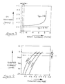
- a plot of the forward characteristics of diode 22 is shown as forward voltage in volts versus forward current in amperes (logarithmic scale) for 75, 25 and -25 degrees celsius. It can be observed from figure 4 that within the range of operation (indicated as B ) the variation of impedance of diode 22 is small. Therefore the impedance of diode 22 may be assigned a constant value without significant loss of measurement accuracy.
- the potential difference between terminals 21 and 29 is the charging voltage at terminal 21 minus the battery voltage at terminal 29 and is equal to the voltage drops across diode 22 and FET 23.
- V charge and V bat are measured values whilst estimated values may be assigned for V diode , R fet and R diode V diode comprises a characteristic voltage called the offset and in addition a voltage varying as the product of the current through and impedance of the diode.
- the offset voltage (V offset ) varies with temperature and can be assigned a value corresponding to the middle of the temperature range.
- the temperature of a battery under charge is altered by the charging process.
- the temperature of the battery and the temperature of the components in the charging circuit are likely to be the same.
- the thermistor in the battery pack at start of charge therefore will provide a good estimate of the temperature of the components of the charging circuit.
- An additional temperature sensor is included in some devices specifically to provide a measure of the ambient temperature in the region of the main electronic components. Where such a sensor is included the variations of assigned values with temperature can be tracked more closely and assigned values adjusted.
- An ambient temperature sensor is shown as numeral 5 of figure 1.
- the value of the voltage offset may be set more accurately by taking into account the temperature of the diode 22 and computing the value from equation 2.
- V offset V hight - V low T hight - T low *T ind + V low
- a sequence of estimated values corresponding to different temperatures across the range may be stored as a look-up table.
- the estimated values used in a series of computations throughout the charging cycle or at specific intervals may be revised to take account of temperature changes.
- An additional measurement point may be made available at terminal 28.
- the voltage drop across diode 22 can then be measured between terminals 21 and 28 and the voltage drop across FET 23 can be measured between terminals 28 and 29.
- a measure of current ( I diode ) through the charging circuit can then be obtained independently from the voltage drop across diode 22 and the estimated value of resistance of diode 22.
- the voltage drop across FET 23 and the estimated value of resistance of FET 23 may be used to obtain independently a measure of the charging current ( I FET ).
Landscapes
- Engineering & Computer Science (AREA)
- Power Engineering (AREA)
- Charge And Discharge Circuits For Batteries Or The Like (AREA)
- Secondary Cells (AREA)
Abstract
Description
- Vcharge
- is the charging voltage at
terminal 21 - Vbat
- is the battery voltage measured at
terminal 29 - Voffset
- is the voltage offset of
diode 22 at a given temperature - Rfet
- is the resistance of
FET 23 - Rdiode
- is the resistance of
diode 22
- Vhigh
- is the diode offset voltage at the top of the temperature range
- Vlow
- is the diode offset voltage at the bottom of the temperature range
- Thigh
- is the highest temperature at which charging will proceed (50°)
- Tlow
- is the lowest temperature at which charging will proceed (0°)
- Tind
- is the measurement from the temperature sensing device (5)
Claims (11)
- A portable communications terminal including a battery and having a charging circuit for connecting an external charger to said battery, said charging circuit comprising a pass device and a diode connected in series and in which levels of charging current are computed from a difference of potential between said external charger and said battery and stored characteristics of said pass device and diode.
- A portable communications terminal as in claim 1 in which the stored characteristics are fixed estimates of diode voltage offset and resistance and pass device impedance .
- A portable communications terminal as in claim 1 in which the stored characteristics are estimated values of diode voltage offset and resistance and pass device impedance set in accordance with measured temperature.
- A portable communications terminal as in claim 3 in which the estimated values are set in accordance with a measurement of temperature at the start of charging.
- A portable communications terminal as in claim 4 in which a measurement of temperature at the start of charging is obtained from a sensor adjacent the battery
- A portable communications terminal as in claims 3 or 4 in which measurement of temperature is obtained from a sensor in the region of the charging circuit.
- A portable communications terminal as in claim 3 in which successive measurements of temperature are obtained throughout the charging cycle.
- A portable communications terminal as in claim 7 in which the estimated values are set in accordance with the successive measurements of temperature obtained throughout the charging cycle.
- A portable communications terminal as in any previous claim in which the estimated values are derived from a look up table.
- A portable communications terminal as in any previous claim in which the pass device is a FET
- A portable communications terminal substantially as hereinbefore described in relation to or as illustrated in the accompanying drawings.
Applications Claiming Priority (2)
| Application Number | Priority Date | Filing Date | Title |
|---|---|---|---|
| GB0113306A GB2376358B (en) | 2001-05-31 | 2001-05-31 | Charging circuits for portable communication terminals |
| GB0113306 | 2001-05-31 |
Publications (2)
| Publication Number | Publication Date |
|---|---|
| EP1263112A2 true EP1263112A2 (en) | 2002-12-04 |
| EP1263112A3 EP1263112A3 (en) | 2004-08-11 |
Family
ID=9915685
Family Applications (1)
| Application Number | Title | Priority Date | Filing Date |
|---|---|---|---|
| EP02252276A Withdrawn EP1263112A3 (en) | 2001-05-31 | 2002-03-27 | Charging circuits for portable communication terminals |
Country Status (2)
| Country | Link |
|---|---|
| EP (1) | EP1263112A3 (en) |
| GB (1) | GB2376358B (en) |
Cited By (1)
| Publication number | Priority date | Publication date | Assignee | Title |
|---|---|---|---|---|
| EP2624406B1 (en) * | 2010-09-30 | 2019-11-06 | NTT DOCOMO, Inc. | Power generator device, portable device, power generation method identification system, power generation method identification method |
Family Cites Families (2)
| Publication number | Priority date | Publication date | Assignee | Title |
|---|---|---|---|---|
| JPH11326400A (en) * | 1998-05-07 | 1999-11-26 | Mitsubishi Electric Corp | Overcurrent detection device |
| US6040683A (en) * | 1999-05-28 | 2000-03-21 | Motorola, Inc. | Battery charger with active feedback voltage controller |
-
2001
- 2001-05-31 GB GB0113306A patent/GB2376358B/en not_active Expired - Fee Related
-
2002
- 2002-03-27 EP EP02252276A patent/EP1263112A3/en not_active Withdrawn
Cited By (1)
| Publication number | Priority date | Publication date | Assignee | Title |
|---|---|---|---|---|
| EP2624406B1 (en) * | 2010-09-30 | 2019-11-06 | NTT DOCOMO, Inc. | Power generator device, portable device, power generation method identification system, power generation method identification method |
Also Published As
| Publication number | Publication date |
|---|---|
| GB2376358B (en) | 2005-01-19 |
| GB2376358A (en) | 2002-12-11 |
| EP1263112A3 (en) | 2004-08-11 |
| GB0113306D0 (en) | 2001-07-25 |
Similar Documents
| Publication | Publication Date | Title |
|---|---|---|
| US8405356B2 (en) | Full charge capacity value correction circuit, battery pack, and charging system | |
| JP3454657B2 (en) | Remaining battery capacity detection method | |
| US6804100B2 (en) | Method and apparatus for protection of batteries | |
| EP1562048B1 (en) | Battery capacity calculating method, battery capacity calculating apparatus, and battery capacity calculating program | |
| US5557192A (en) | Charging apparatus with a compensation circuit | |
| US5926007A (en) | Battery charging apparatus which determines a time to completion of charging | |
| US7425814B2 (en) | Battery pack and remaining battery power calculation method | |
| US20090155674A1 (en) | Battery Pack, Portable Device, Internal Short Detecting Method, and Internal Short Detecting Program | |
| KR101783919B1 (en) | Apparatus and method for estimating open circuit voltage | |
| US20060076929A1 (en) | Method of detecting state-of-charge of battery and power device | |
| CN102741699B (en) | Full-charge capacity correction circuit, charging system, battery pack, and full-charge capacity correction method | |
| EP1577677A1 (en) | Battery apparatus and discharge controlling method of battery apparatus | |
| JP2008253129A (en) | Rapid charging method for lithium secondary battery and electronic device using the same | |
| GB2270983A (en) | Monitoring battery parameters | |
| US20070159135A1 (en) | Battery pack and electronic equipment | |
| JP2011203235A (en) | Method of predicting remaining capacity and run-time of battery device | |
| CN101636872A (en) | Quick charging method of lithium based secondary battery and electronic apparatus employing it | |
| US20040113591A1 (en) | Battery charger | |
| US6023150A (en) | Optimized method for determining remaining life cycles in a rechargeable battery | |
| TW522583B (en) | Electronic machine and control method thereof | |
| KR20010031202A (en) | An identification arrangement and method | |
| US7589495B2 (en) | Battery pack with switching device | |
| JP4086008B2 (en) | Secondary battery remaining capacity ratio calculation method and battery pack | |
| EP1263112A2 (en) | Charging circuits for portable communication terminals | |
| JP3392693B2 (en) | Rechargeable battery capacity detection method |
Legal Events
| Date | Code | Title | Description |
|---|---|---|---|
| PUAI | Public reference made under article 153(3) epc to a published international application that has entered the european phase |
Free format text: ORIGINAL CODE: 0009012 |
|
| AK | Designated contracting states |
Kind code of ref document: A2 Designated state(s): AT BE CH CY DE DK ES FI FR GB GR IE IT LI LU MC NL PT SE TR |
|
| AX | Request for extension of the european patent |
Free format text: AL;LT;LV;MK;RO;SI |
|
| PUAL | Search report despatched |
Free format text: ORIGINAL CODE: 0009013 |
|
| AK | Designated contracting states |
Kind code of ref document: A3 Designated state(s): AT BE CH CY DE DK ES FI FR GB GR IE IT LI LU MC NL PT SE TR |
|
| AX | Request for extension of the european patent |
Extension state: AL LT LV MK RO SI |
|
| RAP1 | Party data changed (applicant data changed or rights of an application transferred) |
Owner name: MATSUSHITA ELECTRIC INDUSTRIAL CO. LTD. |
|
| 17P | Request for examination filed |
Effective date: 20050210 |
|
| 17Q | First examination report despatched |
Effective date: 20050307 |
|
| AKX | Designation fees paid |
Designated state(s): AT BE CH CY DE DK ES FI FR GB GR IE IT LI LU MC NL PT SE TR |
|
| STAA | Information on the status of an ep patent application or granted ep patent |
Free format text: STATUS: THE APPLICATION HAS BEEN WITHDRAWN |
|
| 18W | Application withdrawn |
Effective date: 20050901 |