EP1263096A2 - Improved wide band erbium-doped fiber amplfier (EDFA) - Google Patents
Improved wide band erbium-doped fiber amplfier (EDFA) Download PDFInfo
- Publication number
- EP1263096A2 EP1263096A2 EP01124713A EP01124713A EP1263096A2 EP 1263096 A2 EP1263096 A2 EP 1263096A2 EP 01124713 A EP01124713 A EP 01124713A EP 01124713 A EP01124713 A EP 01124713A EP 1263096 A2 EP1263096 A2 EP 1263096A2
- Authority
- EP
- European Patent Office
- Prior art keywords
- band
- edf
- amplifier
- amplified
- light source
- Prior art date
- Legal status (The legal status is an assumption and is not a legal conclusion. Google has not performed a legal analysis and makes no representation as to the accuracy of the status listed.)
- Granted
Links
Images



Classifications
-
- G—PHYSICS
- G02—OPTICS
- G02B—OPTICAL ELEMENTS, SYSTEMS OR APPARATUS
- G02B6/00—Light guides; Structural details of arrangements comprising light guides and other optical elements, e.g. couplings
-
- H—ELECTRICITY
- H04—ELECTRIC COMMUNICATION TECHNIQUE
- H04B—TRANSMISSION
- H04B10/00—Transmission systems employing electromagnetic waves other than radio-waves, e.g. infrared, visible or ultraviolet light, or employing corpuscular radiation, e.g. quantum communication
- H04B10/29—Repeaters
- H04B10/291—Repeaters in which processing or amplification is carried out without conversion of the main signal from optical form
- H04B10/293—Signal power control
- H04B10/2933—Signal power control considering the whole optical path
- H04B10/2935—Signal power control considering the whole optical path with a cascade of amplifiers
-
- H—ELECTRICITY
- H01—ELECTRIC ELEMENTS
- H01S—DEVICES USING THE PROCESS OF LIGHT AMPLIFICATION BY STIMULATED EMISSION OF RADIATION [LASER] TO AMPLIFY OR GENERATE LIGHT; DEVICES USING STIMULATED EMISSION OF ELECTROMAGNETIC RADIATION IN WAVE RANGES OTHER THAN OPTICAL
- H01S3/00—Lasers, i.e. devices using stimulated emission of electromagnetic radiation in the infrared, visible or ultraviolet wave range
- H01S3/05—Construction or shape of optical resonators; Accommodation of active medium therein; Shape of active medium
- H01S3/06—Construction or shape of active medium
- H01S3/063—Waveguide lasers, i.e. whereby the dimensions of the waveguide are of the order of the light wavelength
- H01S3/067—Fibre lasers
- H01S3/06754—Fibre amplifiers
- H01S3/06758—Tandem amplifiers
-
- H—ELECTRICITY
- H04—ELECTRIC COMMUNICATION TECHNIQUE
- H04B—TRANSMISSION
- H04B10/00—Transmission systems employing electromagnetic waves other than radio-waves, e.g. infrared, visible or ultraviolet light, or employing corpuscular radiation, e.g. quantum communication
- H04B10/25—Arrangements specific to fibre transmission
- H04B10/2507—Arrangements specific to fibre transmission for the reduction or elimination of distortion or dispersion
- H04B10/2537—Arrangements specific to fibre transmission for the reduction or elimination of distortion or dispersion due to scattering processes, e.g. Raman or Brillouin scattering
-
- H—ELECTRICITY
- H01—ELECTRIC ELEMENTS
- H01S—DEVICES USING THE PROCESS OF LIGHT AMPLIFICATION BY STIMULATED EMISSION OF RADIATION [LASER] TO AMPLIFY OR GENERATE LIGHT; DEVICES USING STIMULATED EMISSION OF ELECTROMAGNETIC RADIATION IN WAVE RANGES OTHER THAN OPTICAL
- H01S2301/00—Functional characteristics
- H01S2301/02—ASE (amplified spontaneous emission), noise; Reduction thereof
-
- H—ELECTRICITY
- H01—ELECTRIC ELEMENTS
- H01S—DEVICES USING THE PROCESS OF LIGHT AMPLIFICATION BY STIMULATED EMISSION OF RADIATION [LASER] TO AMPLIFY OR GENERATE LIGHT; DEVICES USING STIMULATED EMISSION OF ELECTROMAGNETIC RADIATION IN WAVE RANGES OTHER THAN OPTICAL
- H01S3/00—Lasers, i.e. devices using stimulated emission of electromagnetic radiation in the infrared, visible or ultraviolet wave range
- H01S3/005—Optical devices external to the laser cavity, specially adapted for lasers, e.g. for homogenisation of the beam or for manipulating laser pulses, e.g. pulse shaping
- H01S3/0064—Anti-reflection devices, e.g. optical isolaters
-
- H—ELECTRICITY
- H01—ELECTRIC ELEMENTS
- H01S—DEVICES USING THE PROCESS OF LIGHT AMPLIFICATION BY STIMULATED EMISSION OF RADIATION [LASER] TO AMPLIFY OR GENERATE LIGHT; DEVICES USING STIMULATED EMISSION OF ELECTROMAGNETIC RADIATION IN WAVE RANGES OTHER THAN OPTICAL
- H01S3/00—Lasers, i.e. devices using stimulated emission of electromagnetic radiation in the infrared, visible or ultraviolet wave range
- H01S3/23—Arrangements of two or more lasers not provided for in groups H01S3/02 - H01S3/22, e.g. tandem arrangements of separate active media
- H01S3/2308—Amplifier arrangements, e.g. MOPA
- H01S3/2325—Multi-pass amplifiers, e.g. regenerative amplifiers
- H01S3/2333—Double-pass amplifiers
Definitions
- the present invention relates to optical communications systems and, in particular, to a wide band optical amplifier.
- an erbium-doped fiber amplifier applicable to an optical communication system has been put to practical use.
- a plurality of optical light signals each having a different wavelength is multiplexed together into a wavelength division multiplexed (WDM) signal light.
- the broad band of the optical amplifier enables each signal light in the wavelength division multiplexed (WDM) signal light to be amplified.
- channel density has been limited by the usable gain bandwidth of the EDFA.
- increasing the EDFA gain bandwidth increases the system capacity while maintaining channel spacing and bit rate per channel.
- FIG. 1 illustrates a schematic view of a broadband EDFA according to a prior art system.
- the input band signals pass through two amplification stages, the C-band and the L-band, then recombined afterward to produce broad optical bandwidth.
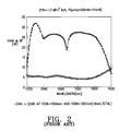
- the L-band fiber amplifier requires a lengthy EDF (188m) as the power conversion efficiency is lower than the conventional C-band EDFAs.
- ASE forward amplified spontaneous emission
- backward ASE light propagating in the direction opposite to the propagation direction of signal light
- ASE forward amplified spontaneous emission
- the noise spectrum ASE generated in the optical amplifier causes problem of precisely monitoring the optical power relating to the signal spectrum. Accordingly, there is a need for a cost-effective optical power amplifier with improved power conversion efficiency and reduced noise.
- the present invention is directed to an optical amplifier with a structure that efficiently utilizes erbium-doped fiber amplifiers (EDFAs) and the associated pump source, and as a consequence provides an increased signal bandwidth with less noise level by utilizing shorter erbium-doped fibers (EDFs) and less pump consumption.
- EDFAs erbium-doped fiber amplifiers
- EDFs erbium-doped fibers
- the present invention relates to an optical amplifier for amplifying optical signals encompassing two or more optical bands.
- the amplifier includes a first erbium-doped fiber amplification pumped by a first pump light source; a second erbium-doped fiber amplifier pumped by a second pump light source; a split section disposed between the first amplifier and the second amplifier stages for splitting optical signals received thereon into a number of sub-band signals; a reflector for reflecting the output of the second amplifier stage back into the second amplifier stage in a reverse direction; a combiner for recombining the amplified light signals to produce an output signal; and, a circulator, provided at the output of the split section, for redirecting the reversely amplified output from the second amplifier stage to the input of the combiner and for preventing ASE generated from the second amplifier stage to travel to the input of the combiner.
- the present invention relates to a method of amplifying optical signals which is performed according to the following steps: passing input optical signals through a first amplifier stage for amplification; splitting the amplified input signals into C-band and L-band signals; amplifying the L-band signal further in a second amplifier stage; redirecting the amplified L-band again back into the second amplifier stage in a reverse direction; and, recombining the further amplified L-band and the C-band to produce an output signal.
- FIG. 3 illustrates a wide band optical amplifier 10 according to a first embodiment of the present invention.
- the inventive amplifier 10 is divided into two amplifier sections, the first amplifier stage, which consist of a first EDF 18 pump by a 980 nm pump laser diode (LD) 14, and the second amplifier stage, which consists of a second EDF 30 pump by a 1480 nm pump laser diode (LD) 26.
- the first amplifier stage which consist of a first EDF 18 pump by a 980 nm pump laser diode (LD) 14
- the second amplifier stage which consists of a second EDF 30 pump by a 1480 nm pump laser diode (LD) 26.
- LD pump laser diode
- the inventive amplifier 10 includes an isolator 12 for directing the input optical signals in a forward direction; a first EDF 18 coupled to the 980 nm pump LD 14 via a 980/1550 nm WSC 16; a first 1550/1590 nm WSC 20 for splitting the amplified optical signals into a C-band and a L-band; an isolator 22 for directing the C-band in a forward direction; a circulator 24 for passing the L-band in a forward direction; a second EDF 30 pump by the 1480 nm pump LD 26 coupled to 1480/1550 nm WSC 28; a reflector 32 for redirecting the amplified L-band and forward ASE back into the second EDF 30 in a reverse direction; and, a second 1550/1590 nm WSC 34 for combining the C-band output from the isolator 22 and the reversely amplified L-band that is redirected by the circulator 24 towards the input of the WSC 34 to produce broad optical bandwidth.
- the C-band ranges from 1530 nm to1560 nm
- the L-band ranges from 1570 nm to 1600 nm.
- these ranges are implementation-dependent, thus they may vary depending upon the design and erbium-doped fiber (EDF).
- EDFs erbium-doped fibers
- the inventive amplifier 10 can support a different length of EDF. Therefore, the length of EDF in the drawing should not impose limitations on the scope of the invention.
- optical signals passing through the isolator 12 and propagating in the forward direction are amplified by the first EDF 18, which is pumped with a 980nm diode laser 14 via the 980/1550 nm WSC 16.
- the function of the isolator 12 to permit light to pass through in only one direction.
- the amplified optical signals are then split into two sub-bands, the C-band and the L-band, through action of the first 1550/1590nm WSC 20.
- the first WSC 20 can take the form of a grating, band splitter, thin film filter, WDM device, and other components that are suitable for reflecting or redirecting one or more band of wavelengths.
- the pump LD 14 preferably emits a pump wavelength pump in a wavelength band centered at about 980 nm; however, 1480 nm pumping is also suitable, as those skilled in the art will appreciate as the conventional pump wavelength for EDFAs.
- the length of first amplifier stage is preferably ⁇ 18 meters. When pumped with light from the pump source 14, some of the pump light is absorbed in the first amplification stage.
- the splitted C-band signals are guided by the isolator 22 to travel only in a forward direction, thus preventing any reflections in the first WSC 20.
- the L-band signals continue to pass forwardly through the second EDF 30, which is forwardly pumped with a 1480 nm diode laser 26 coupled to the 1480/1550nm WSC 28.
- the 1480 nm pump LD 26 preferably emits a pump wavelength in a wavelength band centered at about 1480 nm; however, 980 nm pumping is also suitable, as those skilled in the art will appreciate as the conventional pump wavelength for EDFAs.
- the length of second amplifier stage is preferably ⁇ 95 meters.
- the second amplification stage When pumped with light from the pump source 26, some of the pump light is absorbed in the second amplification stage. After the second amplification, the amplified L-band signals traveling in the forward direction are reflected by the fiber reflector 32. At the same time, the C-band ASE generated during the second amplifier stage and traveling in a forward direction are also reflected by the fiber reflector 26. These reflected L-band and C-band ASE (i.e., the opposite direction of pump light propagation from the pump source 28) are sent back into the second amplifier stage for amplification, then redirected towards the input of the second 1550/1590 nm WSC 34 by the circulator 24.
- L-band and C-band ASE i.e., the opposite direction of pump light propagation from the pump source 28
- the circulator 24 filters out the noise light including the ASE and passes the amplified L-band towards the second 1550/1590 nm WSC 34, thus preventing saturation in C-band ASE at the first amplifier stage and resulting in a suppressed noise due to the C-band ASE.
- the reflected L-band is combined with the C-band outputted from the isolator 22 to produce an output signal.
- FIG. 4 represents a plot of gain and noise figure (dB) vs. wavelength (nm) resulting from an experimental result of the wide band EDFA according the second embodiment depicted in FIG. 3. As shown in FIG. 4, a gain of more than 22dB may be achieved with less optical EDFA and power pump components.
- FIG. 5 illustrates a wide band optical amplifier 40 according to a second embodiment of the present invention.
- optical signals pass through the isolator 42 are amplified by the first EDF 48, which is pumped with a 980 nm diode laser 14 via the 980/1550 nm WSC 46 prior to splitting.
- the length of first EDF 48 is preferably ⁇ 18 meters.
- the amplified optical signals are then divided into two sub-bands, the C-band and the L-band, through action of by first 1550/1590nm WSC 50.
- the reflected C-band signals are guided by the isolator 52 to travel only in a forward direction, thus preventing any reflections in the first WSC 50. Meanwhile, the L-band signals continue to pass forwardly through the second EDF 56, which is backwardly pumped with a 1480 nm diode laser 64 coupled to the 1480/1550nm WSC 58.
- the length of the second EDF 56 is preferably ⁇ 95 meters.
- the amplified L-band signals travelling in the forward direction are reflected by the fiber reflector 32.
- the C-band ASE generated during the first and the second amplifier and passing forwardly are also reflected by the fiber reflector 60.
- These reflected L-band and C-band ASE are sent back into the second amplifier stage for further amplification, and thereafter redirected towards the input of the second 1550/1590 nm WSC 62 via the circulator 54.
- the circulator 54 also filters out the noise light including the ASE traveling in a reverse direction to the first amplifier stage and passes the amplified L-band towards the input of the second 1550/1590 nm WSC 62, thus preventing saturation in C-band ASE and resulting in a suppressed noise due to the C-band ASE.
- the reflected L-band is combined with the C-band outputted from the isolator 52 to produce an output signal.
- FIG. 6 represents a plot of gain and noise figure (dB) vs. wavelength (nm) resulting from an experimental result of the wide band EDFA according the second embodiment depicted in FIG. 5. As shown in FIG. 6, a gain of more than 22dB may be achieved with less optical EDFA and power pump components.
- FIG. 7 illustrates a particular situation to achieve the teaching of the present invention.
- the construction and operation of the third embodiment depicted in FIG. 7 are essentially the same as that described above with respect to FIGs. 3 and 5.
- the only notable difference is that a bi-directional pumping is incorporated in the second amplifier stage. Accordingly, the discussion of similar components described in the preceding paragraphs is omitted to avoid redundancy, as they are described with reference to FIGs. 3 and 5.
- FIG. 8 A working experiment was performed using the inventive wide band optical amplifier structures of FIGs. 3 and 5.
- the first pump laser operating at 980 nm for the C-band and L-band and a second pump laser operating at 1480 nm for the L-band were utilized. From FIG. 8, it can be seen that the gain bandwidth was obtained using a much lower pump power and much shorter EDFs compared to the prior art system. From the test, it can be seen that the inventive structure is more cost-effective with less optical components.
Landscapes
- Physics & Mathematics (AREA)
- Electromagnetism (AREA)
- Engineering & Computer Science (AREA)
- Computer Networks & Wireless Communication (AREA)
- Signal Processing (AREA)
- Optics & Photonics (AREA)
- Plasma & Fusion (AREA)
- General Physics & Mathematics (AREA)
- Lasers (AREA)
Abstract
Description
Claims (16)
- A wide band optical amplifier, comprising:a first erbium-doped fiber amplification stage (EDF1) having a length L1 andpumped by a first pump light source;a second erbium-doped fiber amplifier stage (EDF2) having a length L2 andpumped by a second pump light source;a split section disposed between said EDF1 and said EDF2 for splitting amplified optical signals that enter said split section into a plurality of sub-band signals;a reflector for reflecting the output of said EDF2 back into said second EDF2 in a reverse direction for further amplification; and,a circulator, provided at the output of said split section, for redirecting said reversely amplified output from said second EDF2 to another direction and for preventing an amplified spontaneous emission (ASE) generated in said EDF2 to travel to said another direction.
- The amplifier of claim 1, wherein said first pumping light source is in one of a forward travelling and a backward traveling direction with respect to a direction of amplified signal light.
- The amplifier of claim 1 or 2, wherein said second pumping light source is in one of a forward travelling and backward travelling direction with respect to a direction of amplified signal light.
- The amplifier of one of the claims 1 to 3, further comprising a combiner provided at the end of said another direction for combining said reversely amplified output from said EDF2 and a sub-band signal to produce an output signal.
- The amplifier of one of the claims 1 to 4, further comprising a first isolator permitting input optical signals to propagate in a forward direction toward said EDF1, and a second isolator coupled to the output of said split section for directing one of the sub-band signals to the input of said combiner.
- The amplifier of one of the claims 1 to 5, wherein said second pump light source provides an amount of amplified spontaneous emission (ASE) traveling in a forward direction to be reflected by said reflector, said reflected ASE providing excitation light for said second-band signal amplification by said EDF2.
- The amplifier of one of the claims 1 to 6, wherein said first pump light source provides an amount of amplified spontaneous emission (ASE) traveling in a forward direction, said forward ASE providing excitation light for said EDF1.
- The amplifier of one of the claims 1 to 7, wherein the output of said EDF1 is coupled to the input of said EDF2.
- The amplifier of one of the claims 1 to 8, wherein said L2 is substantially greater than said L1.
- The amplifier of one of the claims 1 to 9, wherein the split section splits the output of EDF1.
- The amplifier of one of the claims 1 to 10, wherein the pump light generated by said first pump light source is in a wavelength band centered at about 980 nm.
- The amplifier of one of the claims 1 to 11, wherein the pump light generated by said second pump light source is in a wavelength band centered at about 1480 nm.
- A method of amplifying optical signals encompassing two or more optical bands, the method comprising the steps of:passing input optical signals through a first amplifier stage (EDF1) for amplification;splitting said amplified signals into C-band and L-band signals;amplifying said L-band signal further in a second amplifier stage (EDF2); redirecting said amplified L-band again back into said EDF2 in a reverse direction for further amplification; and,recombining said further amplified L-band and said C-band to produce an output signal.
- The method of claim 13, wherein said C-band ranges substantially from 1530 nm to 1560 nm.
- The method of claim 13 or 14, wherein said L-band ranges substantially from 1570 nm to 1600 nm.
- The method of one of the claims 13 or 15, wherein said redirection further comprises the step of preventing an amplified spontaneous emission (ASE) generated in said EDF2 to be combined with said C-band.
Applications Claiming Priority (2)
| Application Number | Priority Date | Filing Date | Title |
|---|---|---|---|
| US870598 | 2001-05-31 | ||
| US09/870,598 US6674570B2 (en) | 2001-05-31 | 2001-05-31 | Wide band erbium-doped fiber amplifier (EDFA) |
Publications (3)
| Publication Number | Publication Date |
|---|---|
| EP1263096A2 true EP1263096A2 (en) | 2002-12-04 |
| EP1263096A3 EP1263096A3 (en) | 2003-02-12 |
| EP1263096B1 EP1263096B1 (en) | 2005-02-23 |
Family
ID=25355736
Family Applications (1)
| Application Number | Title | Priority Date | Filing Date |
|---|---|---|---|
| EP01124713A Expired - Lifetime EP1263096B1 (en) | 2001-05-31 | 2001-10-16 | Improved wide band erbium-doped fiber amplifier (EDFA) |
Country Status (6)
| Country | Link |
|---|---|
| US (1) | US6674570B2 (en) |
| EP (1) | EP1263096B1 (en) |
| JP (1) | JP4028218B2 (en) |
| KR (1) | KR100396512B1 (en) |
| CN (1) | CN1171119C (en) |
| DE (1) | DE60109024T2 (en) |
Cited By (2)
| Publication number | Priority date | Publication date | Assignee | Title |
|---|---|---|---|---|
| CN1321348C (en) * | 2003-12-22 | 2007-06-13 | 三星电子株式会社 | Wideband light source |
| CN1726664B (en) * | 2002-12-16 | 2010-09-08 | 阿斯顿光学技术有限公司 | Optical interrogation system and sensor system |
Families Citing this family (28)
| Publication number | Priority date | Publication date | Assignee | Title |
|---|---|---|---|---|
| US6954305B2 (en) * | 2001-09-26 | 2005-10-11 | Sumitomo Electric Industries, Ltd. | Optical amplifier and optical transmission system using it |
| US6781748B2 (en) * | 2001-09-28 | 2004-08-24 | Photon-X, Llc | Long wavelength optical amplifier |
| KR100424630B1 (en) * | 2002-02-14 | 2004-03-25 | 삼성전자주식회사 | Long-band erbium doped fiber amplifier |
| KR100407326B1 (en) * | 2002-02-27 | 2003-11-28 | 삼성전자주식회사 | Wide band erbium doped fiber amplifier for minimizing band crosstalk |
| KR100414914B1 (en) * | 2002-03-05 | 2004-01-13 | 삼성전자주식회사 | Wide band erbium doped fiber amplifier with gain enhancement |
| KR100421135B1 (en) * | 2002-03-11 | 2004-03-04 | 삼성전자주식회사 | Wide band optical fiber amplifier |
| KR100421136B1 (en) * | 2002-03-19 | 2004-03-04 | 삼성전자주식회사 | Wide band erbium doped fiber amplifier and wavelength division multiplexing transmission system therewith |
| KR100474714B1 (en) * | 2002-09-18 | 2005-03-10 | 삼성전자주식회사 | Wideband optical fiber amplifier |
| KR100498938B1 (en) * | 2003-05-20 | 2005-07-04 | 삼성전자주식회사 | Wideband optical fiber amplifier |
| KR100474696B1 (en) * | 2003-05-20 | 2005-03-10 | 삼성전자주식회사 | Wide-band fiber amplifier |
| KR100582542B1 (en) * | 2003-11-11 | 2006-05-23 | 한국전자통신연구원 | Long Wavelength Gain Control Optical Amplifier |
| KR100557170B1 (en) * | 2003-11-14 | 2006-03-03 | 삼성전자주식회사 | Broadband light source |
| US7324268B2 (en) | 2003-11-21 | 2008-01-29 | Bti Photonic Systems Inc. | Optical signal amplifier and method |
| KR100539937B1 (en) * | 2003-12-04 | 2005-12-28 | 삼성전자주식회사 | Dual-port broadband light source |
| KR100622015B1 (en) * | 2004-10-07 | 2006-09-19 | 한국전자통신연구원 | Amplified spontaneous emission (ASE) reflective gain-fixed fiber amplifier |
| DE102005031897B4 (en) * | 2005-07-07 | 2007-10-25 | Siemens Ag | Multi-stage fiber amplifier |
| JP5343722B2 (en) * | 2009-06-15 | 2013-11-13 | 富士通株式会社 | Optical amplifier and polarization dependent gain suppression method for optical amplifier |
| US8578739B2 (en) * | 2010-10-04 | 2013-11-12 | National Applied Research Laboratories | Shorter wavelength photo-annealing apparatus for rare-earth-doped fiber and its optical assemblies under irradiation |
| JP5857517B2 (en) * | 2011-08-11 | 2016-02-10 | 富士通株式会社 | Optical amplifier |
| CN103050870B (en) * | 2012-10-17 | 2015-07-15 | 北京工业大学 | Novel microchip laser supporting optical fiber output |
| DE102013102921B4 (en) * | 2013-03-21 | 2024-02-29 | Günther Heisskanaltechnik Gmbh | Component for an injection molding tool, injection molding tool and method for producing the component |
| CN103618201B (en) * | 2013-12-09 | 2016-06-08 | 北京信息科技大学 | A kind of height smooth C+L band broadband light source of single-ended pumping spectrally compensating |
| CN105258781B (en) * | 2015-09-24 | 2018-11-16 | 中国石油天然气股份有限公司 | Optical fiber vibration detection system and optical fiber vibration detection method |
| TWI668477B (en) * | 2018-08-13 | 2019-08-11 | 建毅科技股份有限公司 | Flexible board optical line device |
| US20220337025A1 (en) * | 2019-09-26 | 2022-10-20 | Nippon Telegraph And Telephone Corporation | Optical amplifier |
| EP4170934A1 (en) * | 2021-10-22 | 2023-04-26 | ADVA Optical Networking SE | Method for reducing the impact of transient effects in an optical network |
| US20240162675A1 (en) * | 2022-11-15 | 2024-05-16 | Ii-Vi Delaware, Inc. | Dual-Band ASE Source Utilizing A Reflective Topology |
| US20240313497A1 (en) * | 2023-03-16 | 2024-09-19 | Ii-Vi Delaware, Inc. | Reflective fiber amplifier in a cascaded topology for operation in c-band and l-band wavelength ranges |
Family Cites Families (11)
| Publication number | Priority date | Publication date | Assignee | Title |
|---|---|---|---|---|
| GB9522943D0 (en) * | 1995-08-05 | 1996-01-10 | Samsung Electronics Co Ltd | Erbium doped fiber amplifier |
| US6049417A (en) | 1997-06-02 | 2000-04-11 | Lucent Technologies Inc. | Wide band optical amplifier |
| KR100265788B1 (en) | 1997-07-03 | 2000-09-15 | 윤종용 | Optical fiber amplifier having high small signal gain |
| US6049418A (en) | 1998-02-06 | 2000-04-11 | Lucent Technologies, Inc. | Noise figure in optical amplifiers with a split-band architecture |
| US6104527A (en) * | 1998-02-20 | 2000-08-15 | Afc Technologies Inc. | High efficiency bandwidth doubled and gain flattened silica fiber amplifier |
| SE522622C2 (en) * | 1998-04-01 | 2004-02-24 | Ericsson Telefon Ab L M | Optical fiber amplifier with controlled gain |
| KR100318942B1 (en) * | 1998-11-24 | 2002-03-20 | 윤종용 | Parallel fluorescent fiber amplifier with high power conversion efficiency |
| KR100330209B1 (en) * | 1999-07-07 | 2002-03-25 | 윤종용 | Wideband optical fiber amplifier and amplifying method thereof |
| CA2279645A1 (en) * | 1999-08-04 | 2001-02-04 | Nortel Networks Corporation | Two-stage modular wide-band optical amplifiers |
| JP2001102666A (en) | 1999-09-28 | 2001-04-13 | Fujitsu Ltd | Optical amplifier |
| KR100415548B1 (en) * | 2001-08-16 | 2004-01-24 | 한국전자통신연구원 | Long-wavelength-band erbium-doped fiber amplifier |
-
2001
- 2001-05-31 US US09/870,598 patent/US6674570B2/en not_active Expired - Fee Related
- 2001-09-29 KR KR10-2001-0060924A patent/KR100396512B1/en not_active Expired - Fee Related
- 2001-10-11 CN CNB011412720A patent/CN1171119C/en not_active Expired - Fee Related
- 2001-10-16 DE DE60109024T patent/DE60109024T2/en not_active Expired - Lifetime
- 2001-10-16 EP EP01124713A patent/EP1263096B1/en not_active Expired - Lifetime
- 2001-12-10 JP JP2001376409A patent/JP4028218B2/en not_active Expired - Fee Related
Cited By (2)
| Publication number | Priority date | Publication date | Assignee | Title |
|---|---|---|---|---|
| CN1726664B (en) * | 2002-12-16 | 2010-09-08 | 阿斯顿光学技术有限公司 | Optical interrogation system and sensor system |
| CN1321348C (en) * | 2003-12-22 | 2007-06-13 | 三星电子株式会社 | Wideband light source |
Also Published As
| Publication number | Publication date |
|---|---|
| DE60109024D1 (en) | 2005-03-31 |
| CN1389758A (en) | 2003-01-08 |
| JP2002368316A (en) | 2002-12-20 |
| JP4028218B2 (en) | 2007-12-26 |
| EP1263096A3 (en) | 2003-02-12 |
| KR20020091747A (en) | 2002-12-06 |
| US20020181090A1 (en) | 2002-12-05 |
| KR100396512B1 (en) | 2003-09-02 |
| US6674570B2 (en) | 2004-01-06 |
| DE60109024T2 (en) | 2005-07-14 |
| EP1263096B1 (en) | 2005-02-23 |
| CN1171119C (en) | 2004-10-13 |
Similar Documents
| Publication | Publication Date | Title |
|---|---|---|
| US6674570B2 (en) | Wide band erbium-doped fiber amplifier (EDFA) | |
| EP1263097B1 (en) | Wide band erbium-doped fiber amplfier (EDFA) | |
| US5673280A (en) | Article comprising low noise optical fiber raman amplifier | |
| JP4717321B2 (en) | Cascaded pumping system for generating distributed Raman amplification in optical fiber communication systems | |
| US6122298A (en) | Multi-wavelength optical pump | |
| US6529317B2 (en) | L-band erbium-doped fiber amplifier pumped by 1530 nm-band pump | |
| KR100424630B1 (en) | Long-band erbium doped fiber amplifier | |
| CN113746552A (en) | Gain equalization in C + L erbium doped fiber amplifiers | |
| JP3884716B2 (en) | Broadband erbium-doped fiber amplifier with gain enhancement | |
| KR100407326B1 (en) | Wide band erbium doped fiber amplifier for minimizing band crosstalk | |
| US6927898B2 (en) | Ultra-wide bandwidth optical amplifier | |
| EP0887955B1 (en) | Robust multi-wavelength optical fiber communication systems | |
| US6862132B1 (en) | Suppression of double rayleigh backscattering and pump reuse in a raman amplifier | |
| KR100446541B1 (en) | Dispersion-compensated raman optical fiber amplifier | |
| US20250364770A1 (en) | Thulium-Doped Fiber Amplifier Including Redirection Of Residual Pump Energy | |
| US20030123141A1 (en) | L band optical amplifier | |
| GB2344210A (en) | A parallel optical fibre amplifier | |
| US20040196535A1 (en) | Long wavelength optical amplifier with C-band seed | |
| GB2326996A (en) | Optical fibre amplifier with absorption medium to reduce noise | |
| JPWO2007034563A1 (en) | Optical amplifier | |
| JP2001168436A (en) | Optical amplifier | |
| JP2001119087A (en) | Er-doped optical fiber amplifier |
Legal Events
| Date | Code | Title | Description |
|---|---|---|---|
| PUAI | Public reference made under article 153(3) epc to a published international application that has entered the european phase |
Free format text: ORIGINAL CODE: 0009012 |
|
| 17P | Request for examination filed |
Effective date: 20011016 |
|
| AK | Designated contracting states |
Kind code of ref document: A2 Designated state(s): AT BE CH CY DE DK ES FI FR GB GR IE IT LI LU MC NL PT SE TR |
|
| AX | Request for extension of the european patent |
Free format text: AL;LT;LV;MK;RO;SI |
|
| PUAL | Search report despatched |
Free format text: ORIGINAL CODE: 0009013 |
|
| AK | Designated contracting states |
Designated state(s): AT BE CH CY DE DK ES FI FR GB GR IE IT LI LU MC NL PT SE TR |
|
| AX | Request for extension of the european patent |
Extension state: AL LT LV MK RO SI |
|
| RIC1 | Information provided on ipc code assigned before grant |
Ipc: 7H 01S 3/091 B Ipc: 7H 04B 10/17 B Ipc: 7H 01S 3/067 A |
|
| 17Q | First examination report despatched |
Effective date: 20030602 |
|
| AKX | Designation fees paid |
Designated state(s): DE FR GB |
|
| GRAP | Despatch of communication of intention to grant a patent |
Free format text: ORIGINAL CODE: EPIDOSNIGR1 |
|
| RTI1 | Title (correction) |
Free format text: IMPROVED WIDE BAND ERBIUM-DOPED FIBER AMPLIFIER (EDFA) |
|
| RIN1 | Information on inventor provided before grant (corrected) |
Inventor name: HWANG, SEONG-TAEK,C/O SAMSUNG ELECTRON. CO., LTD. Inventor name: SONG, KWAN-WOONG,C/O SAMSUNG ELECTRON. CO., LTD. |
|
| GRAS | Grant fee paid |
Free format text: ORIGINAL CODE: EPIDOSNIGR3 |
|
| GRAA | (expected) grant |
Free format text: ORIGINAL CODE: 0009210 |
|
| AK | Designated contracting states |
Kind code of ref document: B1 Designated state(s): DE FR GB |
|
| REG | Reference to a national code |
Ref country code: GB Ref legal event code: FG4D |
|
| REF | Corresponds to: |
Ref document number: 60109024 Country of ref document: DE Date of ref document: 20050331 Kind code of ref document: P |
|
| ET | Fr: translation filed | ||
| PLBE | No opposition filed within time limit |
Free format text: ORIGINAL CODE: 0009261 |
|
| STAA | Information on the status of an ep patent application or granted ep patent |
Free format text: STATUS: NO OPPOSITION FILED WITHIN TIME LIMIT |
|
| 26N | No opposition filed |
Effective date: 20051124 |
|
| PGFP | Annual fee paid to national office [announced via postgrant information from national office to epo] |
Ref country code: DE Payment date: 20091015 Year of fee payment: 9 |
|
| PGFP | Annual fee paid to national office [announced via postgrant information from national office to epo] |
Ref country code: FR Payment date: 20091103 Year of fee payment: 9 Ref country code: GB Payment date: 20091014 Year of fee payment: 9 |
|
| GBPC | Gb: european patent ceased through non-payment of renewal fee |
Effective date: 20101016 |
|
| PG25 | Lapsed in a contracting state [announced via postgrant information from national office to epo] |
Ref country code: FR Free format text: LAPSE BECAUSE OF NON-PAYMENT OF DUE FEES Effective date: 20101102 |
|
| REG | Reference to a national code |
Ref country code: FR Ref legal event code: ST Effective date: 20110630 |
|
| PG25 | Lapsed in a contracting state [announced via postgrant information from national office to epo] |
Ref country code: GB Free format text: LAPSE BECAUSE OF NON-PAYMENT OF DUE FEES Effective date: 20101016 |
|
| REG | Reference to a national code |
Ref country code: DE Ref legal event code: R119 Ref document number: 60109024 Country of ref document: DE Effective date: 20110502 |
|
| PG25 | Lapsed in a contracting state [announced via postgrant information from national office to epo] |
Ref country code: DE Free format text: LAPSE BECAUSE OF NON-PAYMENT OF DUE FEES Effective date: 20110502 |