EP1263085A1 - Omnidirectional antenna - Google Patents
Omnidirectional antenna Download PDFInfo
- Publication number
- EP1263085A1 EP1263085A1 EP02291163A EP02291163A EP1263085A1 EP 1263085 A1 EP1263085 A1 EP 1263085A1 EP 02291163 A EP02291163 A EP 02291163A EP 02291163 A EP02291163 A EP 02291163A EP 1263085 A1 EP1263085 A1 EP 1263085A1
- Authority
- EP
- European Patent Office
- Prior art keywords
- receiving
- transmitting
- line
- radiation
- slot
- Prior art date
- Legal status (The legal status is an assumption and is not a legal conclusion. Google has not performed a legal analysis and makes no representation as to the accuracy of the status listed.)
- Granted
Links
- 230000005855 radiation Effects 0.000 claims abstract description 47
- 230000000295 complement effect Effects 0.000 claims abstract description 3
- 239000000758 substrate Substances 0.000 claims description 10
- 238000005516 engineering process Methods 0.000 claims description 9
- 230000005284 excitation Effects 0.000 description 3
- 230000005540 biological transmission Effects 0.000 description 2
- 230000008878 coupling Effects 0.000 description 2
- 238000010168 coupling process Methods 0.000 description 2
- 238000005859 coupling reaction Methods 0.000 description 2
- 238000004519 manufacturing process Methods 0.000 description 2
- 230000000712 assembly Effects 0.000 description 1
- 238000000429 assembly Methods 0.000 description 1
- 238000004891 communication Methods 0.000 description 1
- 239000004020 conductor Substances 0.000 description 1
- 230000005684 electric field Effects 0.000 description 1
- 238000011835 investigation Methods 0.000 description 1
- 239000002184 metal Substances 0.000 description 1
- 230000007704 transition Effects 0.000 description 1
Images



Classifications
-
- H—ELECTRICITY
- H01—ELECTRIC ELEMENTS
- H01Q—ANTENNAS, i.e. RADIO AERIALS
- H01Q21/00—Antenna arrays or systems
- H01Q21/06—Arrays of individually energised antenna units similarly polarised and spaced apart
- H01Q21/20—Arrays of individually energised antenna units similarly polarised and spaced apart the units being spaced along or adjacent to a curvilinear path
-
- H—ELECTRICITY
- H01—ELECTRIC ELEMENTS
- H01Q—ANTENNAS, i.e. RADIO AERIALS
- H01Q1/00—Details of, or arrangements associated with, antennas
- H01Q1/36—Structural form of radiating elements, e.g. cone, spiral, umbrella; Particular materials used therewith
- H01Q1/38—Structural form of radiating elements, e.g. cone, spiral, umbrella; Particular materials used therewith formed by a conductive layer on an insulating support
-
- H—ELECTRICITY
- H01—ELECTRIC ELEMENTS
- H01Q—ANTENNAS, i.e. RADIO AERIALS
- H01Q13/00—Waveguide horns or mouths; Slot antennas; Leaky-waveguide antennas; Equivalent structures causing radiation along the transmission path of a guided wave
- H01Q13/08—Radiating ends of two-conductor microwave transmission lines, e.g. of coaxial lines, of microstrip lines
-
- H—ELECTRICITY
- H01—ELECTRIC ELEMENTS
- H01Q—ANTENNAS, i.e. RADIO AERIALS
- H01Q13/00—Waveguide horns or mouths; Slot antennas; Leaky-waveguide antennas; Equivalent structures causing radiation along the transmission path of a guided wave
- H01Q13/08—Radiating ends of two-conductor microwave transmission lines, e.g. of coaxial lines, of microstrip lines
- H01Q13/085—Slot-line radiating ends
-
- H—ELECTRICITY
- H01—ELECTRIC ELEMENTS
- H01Q—ANTENNAS, i.e. RADIO AERIALS
- H01Q13/00—Waveguide horns or mouths; Slot antennas; Leaky-waveguide antennas; Equivalent structures causing radiation along the transmission path of a guided wave
- H01Q13/10—Resonant slot antennas
- H01Q13/106—Microstrip slot antennas
-
- H—ELECTRICITY
- H01—ELECTRIC ELEMENTS
- H01Q—ANTENNAS, i.e. RADIO AERIALS
- H01Q19/00—Combinations of primary active antenna elements and units with secondary devices, e.g. with quasi-optical devices, for giving the antenna a desired directional characteristic
- H01Q19/28—Combinations of primary active antenna elements and units with secondary devices, e.g. with quasi-optical devices, for giving the antenna a desired directional characteristic using a secondary device in the form of two or more substantially straight conductive elements
- H01Q19/30—Combinations of primary active antenna elements and units with secondary devices, e.g. with quasi-optical devices, for giving the antenna a desired directional characteristic using a secondary device in the form of two or more substantially straight conductive elements the primary active element being centre-fed and substantially straight, e.g. Yagi antenna
-
- H—ELECTRICITY
- H01—ELECTRIC ELEMENTS
- H01Q—ANTENNAS, i.e. RADIO AERIALS
- H01Q21/00—Antenna arrays or systems
- H01Q21/28—Combinations of substantially independent non-interacting antenna units or systems
Definitions
- the present invention relates to a device for receiving/transmitting electromagnetic waves with omnidirectional radiation of the antenna-type which can be used most particularly in the field of wireless transmissions.
- Figure 1 shows a house with four rooms, three 1, 1', 1" of which have communicating equipment.
- Room 1 has a decoder 2 connected to a television set 3, the decoder being connected to an antenna 4 communicating with a satellite 5.
- the decoder 2/television set 3 assembly is fitted with an antenna 6 belonging to a wireless network capable of communicating via an antenna 9 with a computer 7 and a CD ROM reader 8 placed in another room 1'.
- the antennas most commonly used to meet the requirements for omnidirectional radiation consist of dipole antennas or antennas of the patch type.
- a dipole antenna referenced 20 enables azimuthal omnidirectional coverage to be obtained, as shown in Figure 2, however it has a hole in the axis defined by the radiating element. Consequently, although the dipole antenna is able to communicate with the telephone 21 and the television set 22 located on the same floor, connection with the computer 23 located on an upper floor is not guaranteed.
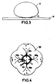
- the printed antennas of the patch type as shown in Figure 3, they comprise schematically a substrate 30 on which a printed patch 31 is produced.
- the patch antenna has hemispherical radiation 32, which limits the coverage to the upper half-space of the earth plane 30.
- the aim of the present invention is therefore to overcome the above drawbacks by proposing a new antenna topology guaranteeing, on the one hand, overall coverage of space and, on the other hand, limited bulk.
- This new topology is based on a type of printed antennas such as the Vivaldi antennas, proposed in French Patent Application No. 98-13855 filed in the name of the applicant.
- the antenna proposed in the aforementioned patent application consists of a coplanar circular arrangement, about a central point, of Vivaldi-type printed radiating elements, making it possible to present several directional beams sequentially over time, the set of beams giving complete 360° coverage of space. Improvements have been made to this type of antennas, in particular, in French Patent Application No. 00-15715 filed in the name of the applicant.
- the pattern of the structure thus excited has areas of zero field in an angular sector surrounding the directions orthogonal to the plane of the substrate, this sector being called a blind zone. These blind zones are defined by the aperture in the H plane of the radiation pattern of an elementary "Vivaldi" antenna.
- the aim of the present invention is therefore to propose an improvement to the structure described above, which makes it possible to eliminate the areas of zero field described above.
- the subject of the present invention is a device for receiving/transmitting electromagnetic waves with omnidirectional radiation of the antenna type comprising a first set of means for receiving/transmitting waves with longitudinal radiation of the printed antenna type, the said means being arranged in order to receive a wide azimuthal sector, characterized in that it further comprises at least a second means for receiving/transmitting waves with transverse radiation of the printed antenna type, the second means having radiation complementary to the radiation of the first means, and means capable of connecting in emission the said first and second wave receiving/transmitting means.
- the means capable of connecting in emission the first set of means for receiving/transmitting waves with longitudinal radiation and the second means for receiving / transmitting waves with transverse radiation consist of a common feed line produced by printed technology.
- each means for receiving/transmitting waves with longitudinal radiation of the printed antenna type consists of a printed slot antenna of the Vivaldi antenna or Yagi antenna type, the antennas hereinabove being arranged at regular intervals around a single point and coplanar so as to be able to radiate over a 360° angle sector.
- the second means for receiving/transmitting waves with transverse radiation of the printed type consists of a slot which is symmetrical with respect to a point or an antenna of the patch type where only a connection to the upper or lower floor is necessary.
- This slot or this patch is circular or square.
- Figure 4 shows schematically a compact antenna of the type described in French Patent Application No. 98-13855 and comprising a feed line as described in French Patent Application No. 00-15715.
- the means for receiving / transmitting longitudinal radiation in this case consist of four printed slot antennas 100a, 100b, 100c, 100d, made on the same substrate 100 and regularly spaced about a central point 101, the four antennas being positioned perpendicularly to each other on the common substrate.
- the slot antennas comprise a slot line which flares progressively from the centre 101 towards the outside of the structure so as to form an antenna of the Vivaldi type.
- Vivaldi antenna The structure and the performance of the Vivaldi antenna are well known to a person skilled in the art and are described in particular in the documents "IEEE Transactions on Antennas and propagations” by S. Prasad and S. Mahapatra; Volume 2 AP 31 No. 3, May 1983 and in "Study of discontinuities in open waveguide - Application to improvement of a radiating source model" by A. Louzir, R. Clequin, S. Toutain and P. Gélin, LestUra C.N.R.S. No. 1329.
- the four antennas 100a, 100b, 100c, 100d are connected to each other via a line 103 made from microstrip technology.
- the end of the microstrip line 103 is at a distance k' ⁇ m /4 from the closest Vivaldi antenna 100d, where k' is an odd number and ⁇ m is given by the equation above.
- the other end of the feed line is connected in emission to means for transmitting signals of a known type, the said means especially comprising a power amplifier.
- the radiation pattern of the structure above has areas of zero field in an angular sector called a blind zone surrounding the directions orthogonal to the plane of the substrate. These blind zones are known since they are defined by the aperture in the H plane of the radiation pattern of an elementary Vivaldi antenna. Consequently, according to the present invention, in order to complete the two coverage regions which are lacking, as shown in Figure 5, an antenna consisting of an annular slot 104 is combined with the antenna with omnidirectional radiation described above. As shown in Figure 5, this antenna with an annular slot is fed by the microstrip line 103 and is at a distance k ⁇ m/2 from the slot of the Vivaldi antenna 100d, preferably k ⁇ m where ⁇ m is defined as above.
- the end of the microstrip line 103 is at a distance k' ⁇ m/4 from the annular slot 104.
- the use of an antenna with an annular slot, as shown in Figure 5, enables the whole device for receiving/transmitting electromagnetic waves with omnidirectional radiation to be produced on the same substrate 100, using microstrip technology, which makes it possible to have an antenna which is compact and easy to produce.
- the radiation of an antenna with an annular slot consists of two lobes distributed on either side of the substrate in which the antenna is etched.
- the coverage zone is complemented with inter-floor connections.
- all the antennas are fed by the same feed line, made with microstrip technology.
- This excitation allows the energy transmitted by each radiating element to be controlled as a function of the impedance thereof. It is therefore possible to generate a perfectly isotropic pattern when all the elements have the same impedance or to favour the radiation in one or more particular sectors.
- FIG. 7 Another embodiment of a device for receiving/transmitting electromagnetic waves with omnidirectional radiation, according to the present invention, will now be described with reference to Figure 7.
- the antennas of the Vivaldi type have been replaced by printed antennas 200a, 200b, 200c, 200d of the Yagi type positioned perpendicularly to each other and symmetrically about a central common point 201.
- These Yagi-type antennas are made on a common substrate 200 using microstrip technology.
- a Yagi-type dipole 200'a, 200'b, 200'c, 200'd combined with two directors 200"a, 200"b, 200"c, 200"d and 200"'a, 200"'b, 200"'c, 200"'d are produced in a metal earth plane.
- the antennas are fed by a common feed line 203 also made from microstrip technology, the length of line between each antenna meeting the same criteria as in the case of Vivaldi-type antennas.
- the second means for receiving / transmitting waves with transverse radiation of the printed antenna type in this case therefore consists of an annular slot 204 fed by the common line 203.
- the operation of the Yagi antennas is identical to the operation of the Vivaldi-type antennas and they provide radiation over a 360° angle sector, the antenna 204 with an annular slot enabling coverage perpendicular to the coverage of the Yagi antennas. Operation of the Yagi-type antennas is known to a person skilled in the art and is in particular described in the article "Coplanar waveguide fed quasi-Yagi antenna", J. Sor, Yongxi Quian and T. Itoh, Electronics Letters, 6 January 2000, Vol. 36, No. 1.
- Yagi-type antennas 300a, 300b, 300c, 300d with a dipole and two directors will be described with reference to Figure 8.
- the antennas are excited by an excitation line 303 made in microstrip technology.
- the Yagi-type antennas operate by slot excitation, that is by electromagnetic coupling between the line 203 and the slots of the antennas, in the present case, the Yagi-type antennas are excited directly by the microstrip line 303.
- the dipoles of the antennas are extended by two microstrip lines 301a-301'a, 301b-301'b, 301c-301'c, 301d-301'd of different length.
- the second transmitting/receiving means consists of an annular slot 304 and the connection via the microstrip line 303 is made as in the embodiment of Figure 7.
- Yagi-type printed antennas 400a, 400b, 400c, 400d of the same type as used above, are used.
- the feed line 403 is a line of coplanar type made in a known manner in the earth plane 402. The operation of a structure of this type is described in the article "First demonstration of a conductor backed coplanar waveguide fed quasi-Yagi antenna" by K.M.K. Leong et al. of the University of California, Los Angeles which appeared in IEEE 2000.
- the second means for transmitting/receiving waves with transverse radiation consists of a slot 404.
- the second means may be produced with an antenna of the patch type.
Landscapes
- Waveguide Aerials (AREA)
- Variable-Direction Aerials And Aerial Arrays (AREA)
- Details Of Aerials (AREA)
- Mobile Radio Communication Systems (AREA)
- Radio Relay Systems (AREA)
Abstract
Description
- The present invention relates to a device for receiving/transmitting electromagnetic waves with omnidirectional radiation of the antenna-type which can be used most particularly in the field of wireless transmissions.
- In the case of domestic networks using wireless transmissions, the antenna design must comply with particular requirements which especially result from the topology of the environment. Thus in this type of application, as shown in Figure 1, communicating devices which may be located at any point in the same room, in different rooms or even on different floors or levels must be considered. For example, Figure 1 shows a house with four rooms, three 1, 1', 1" of which have communicating equipment.
Room 1 has a decoder 2 connected to a television set 3, the decoder being connected to an antenna 4 communicating with a satellite 5. Moreover, the decoder 2/television set 3 assembly is fitted with an antenna 6 belonging to a wireless network capable of communicating via an antenna 9 with a computer 7 and aCD ROM reader 8 placed in another room 1'. These assemblies must also be able to communicate with another television set 10 positioned in aroom 1" on a lower floor. Under these conditions, and so as to ensure complete coverage of the communication space for the purpose of connecting all the terminals of the network, it would appear necessary to design antennas having omnidirectional radiation. - At present, the antennas most commonly used to meet the requirements for omnidirectional radiation consist of dipole antennas or antennas of the patch type.
- A dipole antenna referenced 20 enables azimuthal omnidirectional coverage to be obtained, as shown in Figure 2, however it has a hole in the axis defined by the radiating element. Consequently, although the dipole antenna is able to communicate with the
telephone 21 and the television set 22 located on the same floor, connection with thecomputer 23 located on an upper floor is not guaranteed. - With regard to the printed antennas of the patch type, as shown in Figure 3, they comprise schematically a
substrate 30 on which a printedpatch 31 is produced. As a result, the patch antenna hashemispherical radiation 32, which limits the coverage to the upper half-space of theearth plane 30. - To overcome the coverage problem, several antenna topologies have been proposed. However, they all lead to three-dimensional configurations in which the printed antennas are produced on supports of any shape. Now, these solutions are still bulky and their manufacture tricky for mass production.
- The aim of the present invention is therefore to overcome the above drawbacks by proposing a new antenna topology guaranteeing, on the one hand, overall coverage of space and, on the other hand, limited bulk. This new topology is based on a type of printed antennas such as the Vivaldi antennas, proposed in French Patent Application No. 98-13855 filed in the name of the applicant. The antenna proposed in the aforementioned patent application consists of a coplanar circular arrangement, about a central point, of Vivaldi-type printed radiating elements, making it possible to present several directional beams sequentially over time, the set of beams giving complete 360° coverage of space. Improvements have been made to this type of antennas, in particular, in French Patent Application No. 00-15715 filed in the name of the applicant. In that application, an embodiment allowing an operating mode which is no longer sequential but simultaneous was proposed, that is to say that the set of beams operate at the same time, so as to generate omnidirectional radiation in contrast with the directional radiation of the embodiment described in the previous application. However, the pattern of the structure thus excited has areas of zero field in an angular sector surrounding the directions orthogonal to the plane of the substrate, this sector being called a blind zone. These blind zones are defined by the aperture in the H plane of the radiation pattern of an elementary "Vivaldi" antenna.
- The aim of the present invention is therefore to propose an improvement to the structure described above, which makes it possible to eliminate the areas of zero field described above.
- Consequently, the subject of the present invention is a device for receiving/transmitting electromagnetic waves with omnidirectional radiation of the antenna type comprising a first set of means for receiving/transmitting waves with longitudinal radiation of the printed antenna type, the said means being arranged in order to receive a wide azimuthal sector, characterized in that it further comprises at least a second means for receiving/transmitting waves with transverse radiation of the printed antenna type, the second means having radiation complementary to the radiation of the first means, and means capable of connecting in emission the said first and second wave receiving/transmitting means.
- According to a preferred embodiment, the means capable of connecting in emission the first set of means for receiving/transmitting waves with longitudinal radiation and the second means for receiving / transmitting waves with transverse radiation consist of a common feed line produced by printed technology. This common feed line is formed by a microstrip line or a coplanar line crossing all the slots of the printed slot antennas constituting the first receiving/transmitting set and the second receiving / transmitting means of the slot type, the length of the line between two slots of the first set being equal at the central operating frequency of the system to kλm, the length of the line between the last slot of the first set and the slot of the second receiving/transmitting means being equal at the central operating frequency of the system to kλm/2 and the length of the line between one end of the line and the slot of the second receiving/transmitting means being equal to k'λm/4 where λm = λ0/√εreff where λ0 is the wavelength in vacuo, εreff is the equivalent permittivity of the line, and k and k' are integers. When the second transmitting/receiving means of the slot type consists of a patch, the feed line is directly connected to the patch without additional length.
- Furthermore, each means for receiving/transmitting waves with longitudinal radiation of the printed antenna type consists of a printed slot antenna of the Vivaldi antenna or Yagi antenna type, the antennas hereinabove being arranged at regular intervals around a single point and coplanar so as to be able to radiate over a 360° angle sector.
- Similarly, the second means for receiving/transmitting waves with transverse radiation of the printed type consists of a slot which is symmetrical with respect to a point or an antenna of the patch type where only a connection to the upper or lower floor is necessary. This slot or this patch is circular or square. Thus, according to one characteristic of the invention, the first set of means for receiving/transmitting waves with longitudinal radiation and the second means for receiving/transmitting waves with transverse radiation are produced on the same substrate so as to be symmetric about the same point.
- Other characteristics and advantages of the present invention will become apparent on reading the description hereinafter of various preferred embodiments, this description being made with reference to the appended drawings in which:
- Figure 1, already described, is a schematic sectional view of house furnished with equipment connected together using wireless technology, enabling explanation of the problem that the present invention has to solve,
- Figure 2, already described, is a schematic view explaining the operation of one embodiment according to the prior art,
- Figure 3, already described, is a schematic representation of another type of antenna used in the prior art,
- Figure 4 is a schematic view of a device according to an embodiment of French Patent Application No. 00 15715 which can be used within the scope of the present invention,
- Figure 5 is a top plan view of a first embodiment of the present invention,
- Figure 6 shows the radiation pattern of an annular slot as used in the embodiment of Figure 5,
- Figure 7 is a top plan view of a second embodiment of the present invention,
- Figure 8 is a top plan view of a third embodiment of the present invention, and
- Figure 9 is a bottom plan view of a fourth embodiment of the present invention.
-
- In order to simplify the description in the figures, the same elements bear the same references.
- Figure 4 shows schematically a compact antenna of the type described in French Patent Application No. 98-13855 and comprising a feed line as described in French Patent Application No. 00-15715. In order to receive over an azimuthally wide sector, the means for receiving / transmitting longitudinal radiation in this case consist of four printed
slot antennas same substrate 100 and regularly spaced about a central point 101, the four antennas being positioned perpendicularly to each other on the common substrate. As shown schematically in Figure 4, the slot antennas comprise a slot line which flares progressively from the centre 101 towards the outside of the structure so as to form an antenna of the Vivaldi type. The structure and the performance of the Vivaldi antenna are well known to a person skilled in the art and are described in particular in the documents "IEEE Transactions on Antennas and propagations" by S. Prasad and S. Mahapatra; Volume 2 AP 31 No. 3, May 1983 and in "Study of discontinuities in open waveguide - Application to improvement of a radiating source model" by A. Louzir, R. Clequin, S. Toutain and P. Gélin, LestUra C.N.R.S. No. 1329. - As shown in Figure 4, the four
antennas line 103 made from microstrip technology. This microstrip line makes it possible to produce line/slot transitions by electromagnetic coupling and is positioned so that the length of the line between two slots such as the slot of theantenna 100a and the slot of theantenna 100b is equal at the central operating frequency of the system, to kλm, kλm providing in-phase operation in which λm = λ0/√εreff where λ0 is the wavelength in vacuo, k an integer and εreff the equivalent relative permitivity of the line. Moreover, in order to obtain correct operation in the omnidirectional mode, the end of themicrostrip line 103 is at a distance k'λm/4 from the closest Vivaldiantenna 100d, where k' is an odd number and λm is given by the equation above. The other end of the feed line is connected in emission to means for transmitting signals of a known type, the said means especially comprising a power amplifier. When the slots of the Vivaldi antennas are fed by a feed line of the microstrip type having a length λm or kλm, as shown in Figure 4, in-phase operation of the antennas is obtained, which gives an optimum radiation pattern, as shown in Figure 4 by the arrows E giving the radiated electric field. However, the radiation pattern of the structure above has areas of zero field in an angular sector called a blind zone surrounding the directions orthogonal to the plane of the substrate. These blind zones are known since they are defined by the aperture in the H plane of the radiation pattern of an elementary Vivaldi antenna. Consequently, according to the present invention, in order to complete the two coverage regions which are lacking, as shown in Figure 5, an antenna consisting of anannular slot 104 is combined with the antenna with omnidirectional radiation described above. As shown in Figure 5, this antenna with an annular slot is fed by themicrostrip line 103 and is at a distance kλm/2 from the slot of the Vivaldiantenna 100d, preferably kλm where λm is defined as above. In this case, the end of themicrostrip line 103 is at a distance k'λm/4 from theannular slot 104. The use of an antenna with an annular slot, as shown in Figure 5, enables the whole device for receiving/transmitting electromagnetic waves with omnidirectional radiation to be produced on thesame substrate 100, using microstrip technology, which makes it possible to have an antenna which is compact and easy to produce. - As can be seen in Figure 6, the radiation of an antenna with an annular slot consists of two lobes distributed on either side of the substrate in which the antenna is etched. In this way, with the structure of Figure 5, the coverage zone is complemented with inter-floor connections.
- In addition, in the embodiment described above, all the antennas are fed by the same feed line, made with microstrip technology. This excitation allows the energy transmitted by each radiating element to be controlled as a function of the impedance thereof. It is therefore possible to generate a perfectly isotropic pattern when all the elements have the same impedance or to favour the radiation in one or more particular sectors.
- Another embodiment of a device for receiving/transmitting electromagnetic waves with omnidirectional radiation, according to the present invention, will now be described with reference to Figure 7. In this case, the antennas of the Vivaldi type have been replaced by printed
antennas common point 201. These Yagi-type antennas are made on acommon substrate 200 using microstrip technology. Thus a Yagi-type dipole 200'a, 200'b, 200'c, 200'd combined with twodirectors 200"a, 200"b, 200"c, 200"d and 200"'a, 200"'b, 200"'c, 200"'d are produced in a metal earth plane. As shown in Figure 7, the antennas are fed by acommon feed line 203 also made from microstrip technology, the length of line between each antenna meeting the same criteria as in the case of Vivaldi-type antennas. - As shown in Figure 7, the second means for receiving / transmitting waves with transverse radiation of the printed antenna type in this case therefore consists of an
annular slot 204 fed by thecommon line 203. The operation of the Yagi antennas is identical to the operation of the Vivaldi-type antennas and they provide radiation over a 360° angle sector, theantenna 204 with an annular slot enabling coverage perpendicular to the coverage of the Yagi antennas. Operation of the Yagi-type antennas is known to a person skilled in the art and is in particular described in the article "Coplanar waveguide fed quasi-Yagi antenna", J. Sor, Yongxi Quian and T. Itoh, Electronics Letters, 6 January 2000, Vol. 36, No. 1. - Another embodiment of the invention using Yagi-
type antennas excitation line 303 made in microstrip technology. While in the embodiment of Figure 7, the Yagi-type antennas operate by slot excitation, that is by electromagnetic coupling between theline 203 and the slots of the antennas, in the present case, the Yagi-type antennas are excited directly by themicrostrip line 303. As a result, the dipoles of the antennas are extended by twomicrostrip lines 301a-301'a, 301b-301'b, 301c-301'c, 301d-301'd of different length. The operation of an antenna of this type is known to a person skilled in the art and described in the article "Investigation into the operation of a microstrip fed uniplanar quasi-Yagi antenna" H.J. Song, M.E. Bialkowski, The University of Queensland, Australia -APS 2000. - According to the invention, the second transmitting/receiving means consists of an
annular slot 304 and the connection via themicrostrip line 303 is made as in the embodiment of Figure 7. - In the embodiment of Figure 9, Yagi-type printed
antennas feed line 403 is a line of coplanar type made in a known manner in theearth plane 402. The operation of a structure of this type is described in the article "First demonstration of a conductor backed coplanar waveguide fed quasi-Yagi antenna" by K.M.K. Leong et al. of the University of California, Los Angeles which appeared in IEEE 2000. - In this case also, the second means for transmitting/receiving waves with transverse radiation consists of a slot 404.
- Although unilateral transverse radiation is sufficient, the second means may be produced with an antenna of the patch type.
- It is obvious to a person skilled in the art that the examples above are simply illustrative and can be modified without departing from the scope of the claims.
Claims (9)
- Device for receiving/transmitting electromagnetic waves with omnidirectional radiation of the antenna type comprising:a first set (100a, 100b, 100c, 100d; 200a, 200b, 200c, 200d; 300a, 300b, 300c, 300d; 400a, 400b, 400c, 400d) means for receiving/transmitting waves with longitudinal radiation of the printed antenna type, the said means being arranged in order to receive a wide azimuthal sector, characterized in that it further comprises,at least a second means (104, 204, 304, 404) for receiving/transmitting waves with transverse radiation of the printed antenna type, the second means having radiation complementary to the radiation of the first means, and means (103, 203, 303, 403) capable of connecting in emission the said first and second wave receiving/transmitting means.
- Device according to Claim 1, characterized in that each means for receiving/transmitting waves with longitudinal radiation of the printed antenna type consists of a printed antenna of the Vivaldi antenna or Yagi antenna type.
- Device according to Claim 2, characterized in that the antennas are arranged at regular intervals around a single point and are coplanar so as to be able to radiate over a 360° angle sector.
- Device according to Claims 1 to 3, characterized in that the second means for receiving/transmitting waves of the printed type consists of a slot which is symmetrical with respect to a point or an antenna of the patch type.
- Device according to Claim 4, characterized in that the slot or the patch is circular or square.
- Device according to any one of Claims 1 to 5, characterized in that the first set of means for receiving/transmitting waves with longitudinal radiation and the second means for receiving/transmitting waves with transverse radiation are produced on the same substrate so as to be symmetric about the same point.
- Device according to any one of Claims 1 to 6, characterized in that the means capable of connecting in emission the first set of means for receiving/transmitting waves with longitudinal radiation and the second means for receiving/transmitting waves with transverse radiation consist of a common feed line produced in printed technology.
- Device according to Claim 7, characterized in that the common feed line consists of a microstrip line or a coplanar line crossing all the slots of the printed slot antennas constituting the first receiving/transmitting set and the second receiving / transmitting means of the slot type, the length of the line between two slots of the first set being equal at the central operating frequency of the system to kλm, the length of the line between the last slot of the first set and the slot of the second receiving/transmitting means being equal at the central operating frequency of the system to kλm/2 and the length of the line between the end of the line and the slot of the second receiving/transmitting means being equal to k'λm/4 where λm = λ0/√εreff where λ0 is the wavelength in vacuo and εreff is the equivalent permittivity of the line, k is an integer and k' is another odd integer.
- Device according to Claim 7, characterized in that the common feed line consists of a microstrip line or a coplanar line crossing all of the slots of the printed slot antennas constituting the first receiving / transmitting set, the length of the line between two slots of the first set is kλm and the length of the line between the last slot of the first set and the second receiving/transmitting means of the patch type being equal at the central operating frequency of the system to kλm/2 where λm = λ0/√εreff where λ0 is the wavelength in vacuo, k an integer and εreff the equivalent permittivity of the line.
Applications Claiming Priority (2)
| Application Number | Priority Date | Filing Date | Title |
|---|---|---|---|
| FR0106770A FR2825206A1 (en) | 2001-05-23 | 2001-05-23 | DEVICE FOR RECEIVING AND / OR TRANSMITTING ELECTROMAGNETIC WAVES WITH OMNIDIRECTIONAL RADIATION |
| FR0106770 | 2001-05-23 |
Publications (2)
| Publication Number | Publication Date |
|---|---|
| EP1263085A1 true EP1263085A1 (en) | 2002-12-04 |
| EP1263085B1 EP1263085B1 (en) | 2013-05-01 |
Family
ID=8863574
Family Applications (1)
| Application Number | Title | Priority Date | Filing Date |
|---|---|---|---|
| EP02291163.0A Expired - Lifetime EP1263085B1 (en) | 2001-05-23 | 2002-05-07 | Omnidirectional antenna |
Country Status (7)
| Country | Link |
|---|---|
| US (1) | US6724346B2 (en) |
| EP (1) | EP1263085B1 (en) |
| JP (1) | JP2003037434A (en) |
| KR (1) | KR100873100B1 (en) |
| CN (1) | CN100375336C (en) |
| FR (1) | FR2825206A1 (en) |
| MX (1) | MXPA02005113A (en) |
Cited By (4)
| Publication number | Priority date | Publication date | Assignee | Title |
|---|---|---|---|---|
| FR2925772A1 (en) * | 2007-12-21 | 2009-06-26 | Thomson Licensing Sas | RADIANT MULTI-SECTOR DEVICE HAVING AN OMNIDIRECTIONAL MODE |
| EP2178162A1 (en) * | 2008-10-20 | 2010-04-21 | Sibeam, Inc. | A planar antenna |
| CN1612412B (en) * | 2003-10-31 | 2010-04-28 | 汤姆森许可贸易公司 | High frequency, multiple beam antenna system |
| US8022887B1 (en) | 2006-10-26 | 2011-09-20 | Sibeam, Inc. | Planar antenna |
Families Citing this family (47)
| Publication number | Priority date | Publication date | Assignee | Title |
|---|---|---|---|---|
| EP1557074A4 (en) | 2002-10-22 | 2010-01-13 | Sullivan Jason | Robust customizable computer processing system |
| KR20150040371A (en) | 2002-10-22 | 2015-04-14 | 제이슨 에이. 설리반 | Non-hinged encasement of a device configured to house a processor and consumer electronics device comprising the same |
| CA2503791A1 (en) | 2002-10-22 | 2004-05-06 | Jason A. Sullivan | Non-peripherals processing control module having improved heat dissipating properties |
| US7102571B2 (en) * | 2002-11-08 | 2006-09-05 | Kvh Industries, Inc. | Offset stacked patch antenna and method |
| US6856300B2 (en) * | 2002-11-08 | 2005-02-15 | Kvh Industries, Inc. | Feed network and method for an offset stacked patch antenna array |
| FR2853996A1 (en) * | 2003-04-15 | 2004-10-22 | Thomson Licensing Sa | Antenna system for PCMCIA card, has transmission antenna placed between two reception antennas, where antenna system is placed at edge of PCMCIA card in zone placed exterior to PCMCIA card reader in computer |
| FR2859315A1 (en) * | 2003-08-29 | 2005-03-04 | Thomson Licensing Sa | MULTIBAND PLANAR ANTENNA |
| US6967619B2 (en) | 2004-01-08 | 2005-11-22 | Kvh Industries, Inc. | Low noise block |
| US6977614B2 (en) * | 2004-01-08 | 2005-12-20 | Kvh Industries, Inc. | Microstrip transition and network |
| US7880683B2 (en) * | 2004-08-18 | 2011-02-01 | Ruckus Wireless, Inc. | Antennas with polarization diversity |
| US7292198B2 (en) | 2004-08-18 | 2007-11-06 | Ruckus Wireless, Inc. | System and method for an omnidirectional planar antenna apparatus with selectable elements |
| US7965252B2 (en) * | 2004-08-18 | 2011-06-21 | Ruckus Wireless, Inc. | Dual polarization antenna array with increased wireless coverage |
| US7652632B2 (en) | 2004-08-18 | 2010-01-26 | Ruckus Wireless, Inc. | Multiband omnidirectional planar antenna apparatus with selectable elements |
| US7696946B2 (en) * | 2004-08-18 | 2010-04-13 | Ruckus Wireless, Inc. | Reducing stray capacitance in antenna element switching |
| US8031129B2 (en) * | 2004-08-18 | 2011-10-04 | Ruckus Wireless, Inc. | Dual band dual polarization antenna array |
| US7193562B2 (en) | 2004-11-22 | 2007-03-20 | Ruckus Wireless, Inc. | Circuit board having a peripheral antenna apparatus with selectable antenna elements |
| US7358912B1 (en) | 2005-06-24 | 2008-04-15 | Ruckus Wireless, Inc. | Coverage antenna apparatus with selectable horizontal and vertical polarization elements |
| TWI239681B (en) * | 2004-12-22 | 2005-09-11 | Tatung Co Ltd | Circularly polarized array antenna |
| US7893882B2 (en) | 2007-01-08 | 2011-02-22 | Ruckus Wireless, Inc. | Pattern shaping of RF emission patterns |
| US7646343B2 (en) * | 2005-06-24 | 2010-01-12 | Ruckus Wireless, Inc. | Multiple-input multiple-output wireless antennas |
| KR100701312B1 (en) * | 2005-02-15 | 2007-03-29 | 삼성전자주식회사 | Ultra-wideband antenna with 270 degree coverage and its system |
| US7639106B2 (en) * | 2006-04-28 | 2009-12-29 | Ruckus Wireless, Inc. | PIN diode network for multiband RF coupling |
| US20070293178A1 (en) * | 2006-05-23 | 2007-12-20 | Darin Milton | Antenna Control |
| FR2903216A1 (en) * | 2006-06-28 | 2008-01-04 | Thomson Licensing Sa | IMPROVING DATA MEDIA SUCH AS OPTICAL MEDIA |
| US7427957B2 (en) * | 2007-02-23 | 2008-09-23 | Mark Iv Ivhs, Inc. | Patch antenna |
| JP5004187B2 (en) * | 2008-03-19 | 2012-08-22 | Dxアンテナ株式会社 | Antenna device |
| US8217843B2 (en) * | 2009-03-13 | 2012-07-10 | Ruckus Wireless, Inc. | Adjustment of radiation patterns utilizing a position sensor |
| US8698675B2 (en) * | 2009-05-12 | 2014-04-15 | Ruckus Wireless, Inc. | Mountable antenna elements for dual band antenna |
| JP5615653B2 (en) * | 2009-12-08 | 2014-10-29 | アルプス電気株式会社 | Antenna device |
| US9407012B2 (en) | 2010-09-21 | 2016-08-02 | Ruckus Wireless, Inc. | Antenna with dual polarization and mountable antenna elements |
| FR2965980B1 (en) * | 2010-10-06 | 2013-06-28 | St Microelectronics Sa | ANTENNA ARRAY FOR MICROWAVE, MILLIMETRIC OR TERAHERTZ TYPE WAVE LENGTH SIGNAL TRANSMITTING / RECEIVING DEVICE |
| EP2482237B1 (en) * | 2011-01-26 | 2013-09-04 | Mondi Consumer Packaging Technologies GmbH | Body in the form of a packaging or a moulded part comprising an RFID-Antenna |
| US20120200469A1 (en) * | 2011-02-08 | 2012-08-09 | Henry Cooper | Stacked antenna assembly with removably engageable components |
| WO2012109393A1 (en) | 2011-02-08 | 2012-08-16 | Henry Cooper | High gain frequency step horn antenna |
| WO2012109498A1 (en) | 2011-02-09 | 2012-08-16 | Henry Cooper | Corrugated horn antenna with enhanced frequency range |
| US8756668B2 (en) | 2012-02-09 | 2014-06-17 | Ruckus Wireless, Inc. | Dynamic PSK for hotspots |
| US10186750B2 (en) | 2012-02-14 | 2019-01-22 | Arris Enterprises Llc | Radio frequency antenna array with spacing element |
| US9634403B2 (en) | 2012-02-14 | 2017-04-25 | Ruckus Wireless, Inc. | Radio frequency emission pattern shaping |
| US9092610B2 (en) | 2012-04-04 | 2015-07-28 | Ruckus Wireless, Inc. | Key assignment for a brand |
| US9570799B2 (en) | 2012-09-07 | 2017-02-14 | Ruckus Wireless, Inc. | Multiband monopole antenna apparatus with ground plane aperture |
| EP2974045A4 (en) | 2013-03-15 | 2016-11-09 | Ruckus Wireless Inc | LOW BAND REFLECTOR FOR DOUBLE BAND DIRECTIONAL ANTENNA |
| US9450309B2 (en) | 2013-05-30 | 2016-09-20 | Xi3 | Lobe antenna |
| US9521678B2 (en) * | 2015-03-12 | 2016-12-13 | The Boeing Company | Wireless data concentrators for aircraft data networks |
| JP6434065B2 (en) * | 2017-01-23 | 2018-12-05 | インテル コーポレイション | Antenna structure |
| CN109149080B (en) * | 2017-06-27 | 2020-08-11 | 启碁科技股份有限公司 | communication device |
| TWI754944B (en) * | 2020-03-24 | 2022-02-11 | 日本商英幸技術股份有限公司 | Electromagnetic wave transceiving apparatus |
| WO2024097188A1 (en) * | 2022-10-31 | 2024-05-10 | John Mezzalingua Associates, LLC. | Ultra-flat 2x2 mimo broadband antenna |
Citations (4)
| Publication number | Priority date | Publication date | Assignee | Title |
|---|---|---|---|---|
| EP0301216A2 (en) * | 1987-07-29 | 1989-02-01 | Ball Corporation | Broadband notch antenna |
| GB2272575A (en) * | 1992-11-02 | 1994-05-18 | Gec Ferranti Defence Syst | Dual band antenna |
| CA2210080A1 (en) * | 1997-07-08 | 1999-01-08 | Lotfollah Shafai | Microstrip line fed microstrip end-fire antenna |
| FR2785476A1 (en) * | 1998-11-04 | 2000-05-05 | Thomson Multimedia Sa | Multiple beam wireless reception system has circular multiple beam printed circuit with beam switching mechanism, mounted on camera |
Family Cites Families (6)
| Publication number | Priority date | Publication date | Assignee | Title |
|---|---|---|---|---|
| JPH02905A (en) * | 1988-05-23 | 1990-01-05 | Nippon Telegr & Teleph Corp <Ntt> | Filter element |
| JPH02179102A (en) * | 1988-12-29 | 1990-07-12 | Sony Corp | Microstrip antenna |
| FR2709833B1 (en) * | 1993-09-07 | 1995-10-20 | Alcatel Espace | Broadband and low band listening instrument for space applications. |
| JPH0897632A (en) * | 1994-09-21 | 1996-04-12 | Nippon Telegr & Teleph Corp <Ntt> | Wireless transceiver |
| US6445354B1 (en) * | 1999-08-16 | 2002-09-03 | Novatel, Inc. | Aperture coupled slot array antenna |
| US6366254B1 (en) * | 2000-03-15 | 2002-04-02 | Hrl Laboratories, Llc | Planar antenna with switched beam diversity for interference reduction in a mobile environment |
-
2001
- 2001-05-23 FR FR0106770A patent/FR2825206A1/en active Pending
-
2002
- 2002-05-07 EP EP02291163.0A patent/EP1263085B1/en not_active Expired - Lifetime
- 2002-05-15 CN CNB021198527A patent/CN100375336C/en not_active Expired - Fee Related
- 2002-05-20 KR KR1020020027797A patent/KR100873100B1/en not_active Expired - Fee Related
- 2002-05-21 US US10/152,665 patent/US6724346B2/en not_active Expired - Lifetime
- 2002-05-22 MX MXPA02005113A patent/MXPA02005113A/en active IP Right Grant
- 2002-05-22 JP JP2002147903A patent/JP2003037434A/en active Pending
Patent Citations (4)
| Publication number | Priority date | Publication date | Assignee | Title |
|---|---|---|---|---|
| EP0301216A2 (en) * | 1987-07-29 | 1989-02-01 | Ball Corporation | Broadband notch antenna |
| GB2272575A (en) * | 1992-11-02 | 1994-05-18 | Gec Ferranti Defence Syst | Dual band antenna |
| CA2210080A1 (en) * | 1997-07-08 | 1999-01-08 | Lotfollah Shafai | Microstrip line fed microstrip end-fire antenna |
| FR2785476A1 (en) * | 1998-11-04 | 2000-05-05 | Thomson Multimedia Sa | Multiple beam wireless reception system has circular multiple beam printed circuit with beam switching mechanism, mounted on camera |
Non-Patent Citations (1)
| Title |
|---|
| VAUGHAN M J ET AL: "28 GHZ OMNI-DIRECTIONAL QUASI-OPTICAL TRANSMITTER ARRAY", IEEE TRANSACTIONS ON MICROWAVE THEORY AND TECHNIQUES, IEEE INC. NEW YORK, US, vol. 43, no. 10, 1 October 1995 (1995-10-01), pages 2507 - 2509, XP000530205, ISSN: 0018-9480 * |
Cited By (6)
| Publication number | Priority date | Publication date | Assignee | Title |
|---|---|---|---|---|
| CN1612412B (en) * | 2003-10-31 | 2010-04-28 | 汤姆森许可贸易公司 | High frequency, multiple beam antenna system |
| US8022887B1 (en) | 2006-10-26 | 2011-09-20 | Sibeam, Inc. | Planar antenna |
| FR2925772A1 (en) * | 2007-12-21 | 2009-06-26 | Thomson Licensing Sas | RADIANT MULTI-SECTOR DEVICE HAVING AN OMNIDIRECTIONAL MODE |
| WO2009080418A1 (en) * | 2007-12-21 | 2009-07-02 | Thomson Licensing | Multi-sector radiating device with an omni-directional mode |
| US8593361B2 (en) | 2007-12-21 | 2013-11-26 | Thomson Licensing | Multi-sector radiating device with an omni-directional mode |
| EP2178162A1 (en) * | 2008-10-20 | 2010-04-21 | Sibeam, Inc. | A planar antenna |
Also Published As
| Publication number | Publication date |
|---|---|
| KR20020090135A (en) | 2002-11-30 |
| KR100873100B1 (en) | 2008-12-09 |
| JP2003037434A (en) | 2003-02-07 |
| MXPA02005113A (en) | 2004-08-11 |
| CN100375336C (en) | 2008-03-12 |
| EP1263085B1 (en) | 2013-05-01 |
| CN1387283A (en) | 2002-12-25 |
| US20030020663A1 (en) | 2003-01-30 |
| FR2825206A1 (en) | 2002-11-29 |
| US6724346B2 (en) | 2004-04-20 |
Similar Documents
| Publication | Publication Date | Title |
|---|---|---|
| EP1263085B1 (en) | Omnidirectional antenna | |
| Ullah et al. | A novel snowflake fractal antenna for dual-beam applications in 28 GHz band | |
| CN109687116B (en) | C-band miniaturized broadband wide-beam circularly polarized microstrip antenna | |
| US7310065B2 (en) | Undersampled microstrip array using multilevel and space-filling shaped elements | |
| US6642898B2 (en) | Fractal cross slot antenna | |
| Tang et al. | A study of 28 GHz, planar, multilayered, electrically small, broadside radiating, Huygens source antennas | |
| EP3278398B1 (en) | Sparse phase-mode planar feed for circular arrays | |
| US7064725B2 (en) | Conical beam cross-slot antenna | |
| US7239288B2 (en) | Access point antenna for a wireless local area network | |
| US6967625B1 (en) | E-plane omni-directional antenna | |
| WO2019100376A1 (en) | Omnidirectional array antenna and beamforming method therefor | |
| JP2004120733A (en) | Stripline parallel-series-fed proximity coupled cavity backed patch antenna array | |
| JP5836097B2 (en) | Multi-beam antenna system | |
| Feng et al. | Analysis of double‐Xi‐shaped millimetre‐wave patch antenna backed by a high‐order‐mode cavity using characteristic mode design | |
| Xing et al. | Dual-band quad-polarized anti-multipath interference antenna for IoT indoor backscatter positioning | |
| Shishkin | Research of a wideband dual-polarization microstrip antenna array on a suspended substrate with irregular arrangement of elements | |
| Schandy et al. | Enhancing parasitic interference directional antennas with multiple director elements | |
| US11189939B2 (en) | Dual-polarized wide-bandwidth antenna | |
| US8593361B2 (en) | Multi-sector radiating device with an omni-directional mode | |
| CN220341510U (en) | Broadband polarized tightly-coupled dipole transmission array antenna | |
| CN115954657B (en) | Millimeter-wave antenna with reconfigurable radiation pattern | |
| CN102570052B (en) | The compact systems of multi-beam antenna | |
| US10862220B2 (en) | Antenna for use in electronic communication systems | |
| US11482794B1 (en) | Slot-fed unit cell and current sheet array | |
| CN118801083A (en) | Antenna and communication device |
Legal Events
| Date | Code | Title | Description |
|---|---|---|---|
| PUAI | Public reference made under article 153(3) epc to a published international application that has entered the european phase |
Free format text: ORIGINAL CODE: 0009012 |
|
| AK | Designated contracting states |
Kind code of ref document: A1 Designated state(s): AT BE CH CY DE DK ES FI FR GB GR IE IT LI LU MC NL PT SE TR |
|
| AX | Request for extension of the european patent |
Free format text: AL;LT;LV;MK;RO;SI |
|
| RIN1 | Information on inventor provided before grant (corrected) |
Inventor name: LOUZIR, ALI Inventor name: LE BOLZER, FRANCOISE |
|
| 17P | Request for examination filed |
Effective date: 20030602 |
|
| AKX | Designation fees paid |
Designated state(s): AT BE CH CY DE DK ES FI FR GB GR IE IT LI LU MC NL PT SE TR |
|
| RAP1 | Party data changed (applicant data changed or rights of an application transferred) |
Owner name: THOMSON LICENSING |
|
| 17Q | First examination report despatched |
Effective date: 20080508 |
|
| RAP1 | Party data changed (applicant data changed or rights of an application transferred) |
Owner name: THOMSON LICENSING |
|
| GRAP | Despatch of communication of intention to grant a patent |
Free format text: ORIGINAL CODE: EPIDOSNIGR1 |
|
| GRAS | Grant fee paid |
Free format text: ORIGINAL CODE: EPIDOSNIGR3 |
|
| GRAA | (expected) grant |
Free format text: ORIGINAL CODE: 0009210 |
|
| AK | Designated contracting states |
Kind code of ref document: B1 Designated state(s): AT BE CH CY DE DK ES FI FR GB GR IE IT LI LU MC NL PT SE TR |
|
| REG | Reference to a national code |
Ref country code: GB Ref legal event code: FG4D |
|
| REG | Reference to a national code |
Ref country code: CH Ref legal event code: EP Ref country code: AT Ref legal event code: REF Ref document number: 610432 Country of ref document: AT Kind code of ref document: T Effective date: 20130515 |
|
| REG | Reference to a national code |
Ref country code: IE Ref legal event code: FG4D |
|
| REG | Reference to a national code |
Ref country code: GB Ref legal event code: 746 Effective date: 20130510 |
|
| REG | Reference to a national code |
Ref country code: DE Ref legal event code: R096 Ref document number: 60244896 Country of ref document: DE Effective date: 20130704 Ref country code: DE Ref legal event code: R084 Ref document number: 60244896 Country of ref document: DE Effective date: 20130504 |
|
| REG | Reference to a national code |
Ref country code: AT Ref legal event code: MK05 Ref document number: 610432 Country of ref document: AT Kind code of ref document: T Effective date: 20130501 |
|
| REG | Reference to a national code |
Ref country code: NL Ref legal event code: VDEP Effective date: 20130501 |
|
| PG25 | Lapsed in a contracting state [announced via postgrant information from national office to epo] |
Ref country code: AT Free format text: LAPSE BECAUSE OF FAILURE TO SUBMIT A TRANSLATION OF THE DESCRIPTION OR TO PAY THE FEE WITHIN THE PRESCRIBED TIME-LIMIT Effective date: 20130501 Ref country code: FI Free format text: LAPSE BECAUSE OF FAILURE TO SUBMIT A TRANSLATION OF THE DESCRIPTION OR TO PAY THE FEE WITHIN THE PRESCRIBED TIME-LIMIT Effective date: 20130501 Ref country code: GR Free format text: LAPSE BECAUSE OF FAILURE TO SUBMIT A TRANSLATION OF THE DESCRIPTION OR TO PAY THE FEE WITHIN THE PRESCRIBED TIME-LIMIT Effective date: 20130802 Ref country code: SE Free format text: LAPSE BECAUSE OF FAILURE TO SUBMIT A TRANSLATION OF THE DESCRIPTION OR TO PAY THE FEE WITHIN THE PRESCRIBED TIME-LIMIT Effective date: 20130501 Ref country code: ES Free format text: LAPSE BECAUSE OF FAILURE TO SUBMIT A TRANSLATION OF THE DESCRIPTION OR TO PAY THE FEE WITHIN THE PRESCRIBED TIME-LIMIT Effective date: 20130812 Ref country code: PT Free format text: LAPSE BECAUSE OF FAILURE TO SUBMIT A TRANSLATION OF THE DESCRIPTION OR TO PAY THE FEE WITHIN THE PRESCRIBED TIME-LIMIT Effective date: 20130902 |
|
| REG | Reference to a national code |
Ref country code: CH Ref legal event code: PL |
|
| PG25 | Lapsed in a contracting state [announced via postgrant information from national office to epo] |
Ref country code: MC Free format text: LAPSE BECAUSE OF FAILURE TO SUBMIT A TRANSLATION OF THE DESCRIPTION OR TO PAY THE FEE WITHIN THE PRESCRIBED TIME-LIMIT Effective date: 20130501 Ref country code: DK Free format text: LAPSE BECAUSE OF FAILURE TO SUBMIT A TRANSLATION OF THE DESCRIPTION OR TO PAY THE FEE WITHIN THE PRESCRIBED TIME-LIMIT Effective date: 20130501 Ref country code: CH Free format text: LAPSE BECAUSE OF NON-PAYMENT OF DUE FEES Effective date: 20130531 Ref country code: LI Free format text: LAPSE BECAUSE OF NON-PAYMENT OF DUE FEES Effective date: 20130531 Ref country code: BE Free format text: LAPSE BECAUSE OF FAILURE TO SUBMIT A TRANSLATION OF THE DESCRIPTION OR TO PAY THE FEE WITHIN THE PRESCRIBED TIME-LIMIT Effective date: 20130501 |
|
| REG | Reference to a national code |
Ref country code: IE Ref legal event code: MM4A |
|
| PG25 | Lapsed in a contracting state [announced via postgrant information from national office to epo] |
Ref country code: NL Free format text: LAPSE BECAUSE OF FAILURE TO SUBMIT A TRANSLATION OF THE DESCRIPTION OR TO PAY THE FEE WITHIN THE PRESCRIBED TIME-LIMIT Effective date: 20130501 Ref country code: IT Free format text: LAPSE BECAUSE OF FAILURE TO SUBMIT A TRANSLATION OF THE DESCRIPTION OR TO PAY THE FEE WITHIN THE PRESCRIBED TIME-LIMIT Effective date: 20130501 |
|
| PLBE | No opposition filed within time limit |
Free format text: ORIGINAL CODE: 0009261 |
|
| STAA | Information on the status of an ep patent application or granted ep patent |
Free format text: STATUS: NO OPPOSITION FILED WITHIN TIME LIMIT |
|
| 26N | No opposition filed |
Effective date: 20140204 |
|
| PG25 | Lapsed in a contracting state [announced via postgrant information from national office to epo] |
Ref country code: IE Free format text: LAPSE BECAUSE OF NON-PAYMENT OF DUE FEES Effective date: 20130507 |
|
| REG | Reference to a national code |
Ref country code: DE Ref legal event code: R097 Ref document number: 60244896 Country of ref document: DE Effective date: 20140204 |
|
| PG25 | Lapsed in a contracting state [announced via postgrant information from national office to epo] |
Ref country code: TR Free format text: LAPSE BECAUSE OF FAILURE TO SUBMIT A TRANSLATION OF THE DESCRIPTION OR TO PAY THE FEE WITHIN THE PRESCRIBED TIME-LIMIT Effective date: 20130501 Ref country code: CY Free format text: LAPSE BECAUSE OF FAILURE TO SUBMIT A TRANSLATION OF THE DESCRIPTION OR TO PAY THE FEE WITHIN THE PRESCRIBED TIME-LIMIT Effective date: 20130501 |
|
| PG25 | Lapsed in a contracting state [announced via postgrant information from national office to epo] |
Ref country code: LU Free format text: LAPSE BECAUSE OF NON-PAYMENT OF DUE FEES Effective date: 20130507 |
|
| REG | Reference to a national code |
Ref country code: FR Ref legal event code: PLFP Year of fee payment: 15 |
|
| REG | Reference to a national code |
Ref country code: FR Ref legal event code: PLFP Year of fee payment: 16 |
|
| REG | Reference to a national code |
Ref country code: DE Ref legal event code: R082 Ref document number: 60244896 Country of ref document: DE Representative=s name: HOFSTETTER, SCHURACK & PARTNER - PATENT- UND R, DE Ref country code: DE Ref legal event code: R082 Ref document number: 60244896 Country of ref document: DE Representative=s name: HOFSTETTER, SCHURACK & PARTNER PATENT- UND REC, DE |
|
| REG | Reference to a national code |
Ref country code: FR Ref legal event code: PLFP Year of fee payment: 17 |
|
| PGFP | Annual fee paid to national office [announced via postgrant information from national office to epo] |
Ref country code: DE Payment date: 20190510 Year of fee payment: 18 |
|
| PGFP | Annual fee paid to national office [announced via postgrant information from national office to epo] |
Ref country code: FR Payment date: 20190531 Year of fee payment: 18 |
|
| PGFP | Annual fee paid to national office [announced via postgrant information from national office to epo] |
Ref country code: GB Payment date: 20190516 Year of fee payment: 18 |
|
| REG | Reference to a national code |
Ref country code: DE Ref legal event code: R119 Ref document number: 60244896 Country of ref document: DE |
|
| GBPC | Gb: european patent ceased through non-payment of renewal fee |
Effective date: 20200507 |
|
| PG25 | Lapsed in a contracting state [announced via postgrant information from national office to epo] |
Ref country code: GB Free format text: LAPSE BECAUSE OF NON-PAYMENT OF DUE FEES Effective date: 20200507 Ref country code: FR Free format text: LAPSE BECAUSE OF NON-PAYMENT OF DUE FEES Effective date: 20200531 |
|
| PG25 | Lapsed in a contracting state [announced via postgrant information from national office to epo] |
Ref country code: DE Free format text: LAPSE BECAUSE OF NON-PAYMENT OF DUE FEES Effective date: 20201201 |
|
| P01 | Opt-out of the competence of the unified patent court (upc) registered |
Effective date: 20230526 |