EP1261037A1 - Package for optoelectronic device and method therefor - Google Patents
Package for optoelectronic device and method therefor Download PDFInfo
- Publication number
- EP1261037A1 EP1261037A1 EP01304660A EP01304660A EP1261037A1 EP 1261037 A1 EP1261037 A1 EP 1261037A1 EP 01304660 A EP01304660 A EP 01304660A EP 01304660 A EP01304660 A EP 01304660A EP 1261037 A1 EP1261037 A1 EP 1261037A1
- Authority
- EP
- European Patent Office
- Prior art keywords
- oxygen
- package
- housing
- gaseous atmosphere
- sensitive material
- Prior art date
- Legal status (The legal status is an assumption and is not a legal conclusion. Google has not performed a legal analysis and makes no representation as to the accuracy of the status listed.)
- Withdrawn
Links
- 238000000034 method Methods 0.000 title claims description 11
- 230000005693 optoelectronics Effects 0.000 title claims description 10
- QVGXLLKOCUKJST-UHFFFAOYSA-N atomic oxygen Chemical compound [O] QVGXLLKOCUKJST-UHFFFAOYSA-N 0.000 claims abstract description 62
- 239000001301 oxygen Substances 0.000 claims abstract description 62
- 229910052760 oxygen Inorganic materials 0.000 claims abstract description 62
- 239000000463 material Substances 0.000 claims abstract description 22
- 239000012298 atmosphere Substances 0.000 claims description 33
- 238000011109 contamination Methods 0.000 claims description 5
- 230000003287 optical effect Effects 0.000 claims description 5
- 239000007789 gas Substances 0.000 claims description 4
- 239000002861 polymer material Substances 0.000 claims description 3
- 239000013307 optical fiber Substances 0.000 description 11
- IJGRMHOSHXDMSA-UHFFFAOYSA-N Atomic nitrogen Chemical compound N#N IJGRMHOSHXDMSA-UHFFFAOYSA-N 0.000 description 6
- 239000004065 semiconductor Substances 0.000 description 5
- UQSXHKLRYXJYBZ-UHFFFAOYSA-N Iron oxide Chemical compound [Fe]=O UQSXHKLRYXJYBZ-UHFFFAOYSA-N 0.000 description 4
- 230000008878 coupling Effects 0.000 description 3
- 238000010168 coupling process Methods 0.000 description 3
- 238000005859 coupling reaction Methods 0.000 description 3
- 238000010586 diagram Methods 0.000 description 3
- 239000011261 inert gas Substances 0.000 description 3
- 229910052757 nitrogen Inorganic materials 0.000 description 3
- 230000001681 protective effect Effects 0.000 description 3
- XKRFYHLGVUSROY-UHFFFAOYSA-N Argon Chemical compound [Ar] XKRFYHLGVUSROY-UHFFFAOYSA-N 0.000 description 2
- 238000010276 construction Methods 0.000 description 2
- 239000012535 impurity Substances 0.000 description 2
- 238000007789 sealing Methods 0.000 description 2
- 229910052786 argon Inorganic materials 0.000 description 1
- 238000006243 chemical reaction Methods 0.000 description 1
- 230000005670 electromagnetic radiation Effects 0.000 description 1
- 230000007774 longterm Effects 0.000 description 1
- 238000004519 manufacturing process Methods 0.000 description 1
- 239000012299 nitrogen atmosphere Substances 0.000 description 1
- 238000004806 packaging method and process Methods 0.000 description 1
- 239000002574 poison Substances 0.000 description 1
- 231100000614 poison Toxicity 0.000 description 1
- 238000003466 welding Methods 0.000 description 1
Images
Classifications
-
- H—ELECTRICITY
- H10—SEMICONDUCTOR DEVICES; ELECTRIC SOLID-STATE DEVICES NOT OTHERWISE PROVIDED FOR
- H10F—INORGANIC SEMICONDUCTOR DEVICES SENSITIVE TO INFRARED RADIATION, LIGHT, ELECTROMAGNETIC RADIATION OF SHORTER WAVELENGTH OR CORPUSCULAR RADIATION
- H10F77/00—Constructional details of devices covered by this subclass
- H10F77/40—Optical elements or arrangements
- H10F77/407—Optical elements or arrangements indirectly associated with the devices
-
- H—ELECTRICITY
- H01—ELECTRIC ELEMENTS
- H01S—DEVICES USING THE PROCESS OF LIGHT AMPLIFICATION BY STIMULATED EMISSION OF RADIATION [LASER] TO AMPLIFY OR GENERATE LIGHT; DEVICES USING STIMULATED EMISSION OF ELECTROMAGNETIC RADIATION IN WAVE RANGES OTHER THAN OPTICAL
- H01S5/00—Semiconductor lasers
- H01S5/005—Optical components external to the laser cavity, specially adapted therefor, e.g. for homogenisation or merging of the beams or for manipulating laser pulses, e.g. pulse shaping
- H01S5/0085—Optical components external to the laser cavity, specially adapted therefor, e.g. for homogenisation or merging of the beams or for manipulating laser pulses, e.g. pulse shaping for modulating the output, i.e. the laser beam is modulated outside the laser cavity
-
- H—ELECTRICITY
- H01—ELECTRIC ELEMENTS
- H01S—DEVICES USING THE PROCESS OF LIGHT AMPLIFICATION BY STIMULATED EMISSION OF RADIATION [LASER] TO AMPLIFY OR GENERATE LIGHT; DEVICES USING STIMULATED EMISSION OF ELECTROMAGNETIC RADIATION IN WAVE RANGES OTHER THAN OPTICAL
- H01S5/00—Semiconductor lasers
- H01S5/02—Structural details or components not essential to laser action
- H01S5/022—Mountings; Housings
- H01S5/02235—Getter material for absorbing contamination
-
- H—ELECTRICITY
- H01—ELECTRIC ELEMENTS
- H01S—DEVICES USING THE PROCESS OF LIGHT AMPLIFICATION BY STIMULATED EMISSION OF RADIATION [LASER] TO AMPLIFY OR GENERATE LIGHT; DEVICES USING STIMULATED EMISSION OF ELECTROMAGNETIC RADIATION IN WAVE RANGES OTHER THAN OPTICAL
- H01S5/00—Semiconductor lasers
- H01S5/02—Structural details or components not essential to laser action
- H01S5/022—Mountings; Housings
- H01S5/0225—Out-coupling of light
- H01S5/02251—Out-coupling of light using optical fibres
-
- H—ELECTRICITY
- H10—SEMICONDUCTOR DEVICES; ELECTRIC SOLID-STATE DEVICES NOT OTHERWISE PROVIDED FOR
- H10H—INORGANIC LIGHT-EMITTING SEMICONDUCTOR DEVICES HAVING POTENTIAL BARRIERS
- H10H20/00—Individual inorganic light-emitting semiconductor devices having potential barriers, e.g. light-emitting diodes [LED]
- H10H20/80—Constructional details
- H10H20/85—Packages
- H10H20/8506—Containers
Definitions
- the present invention relates to a package for an optoelectronic device, the package being of the type used to store oxygen sensitive materials, for example an oxygen sensitive plastic material, such as an optoelectronic modulator formed from the plastic material, in a protective atmosphere, the protective atmosphere being substantially oxygen-free.
- the present invention also relates to a method of removing oxygen from the protective atmosphere of the above package.
- a package for an optoelectronic modulator comprises a housing having the modulator mounted on an optical platform within the housing.
- the housing is filled with any gas that does not react with or 'poison' the modulator, the gas preferably having a high atomic mass, for example Nitrogen, Zeon or Argon.
- the housing comprises an oxygen-free atmosphere.
- the oxygen-free atmosphere is maintained by hermetically sealing the housing. However, the hermetic seal of the housing can fail leading to ingress of oxygen into the housing, thereby contaminating the oxygen-free atmosphere.
- US 5, 392, 305, US 5, 629, 952 and US 5, 770, 473 disclose the positive presence of oxygen in controlled amounts in the atmosphere within the housing in order to provide stable, long term, continuous operation of a high-power semiconductor laser.
- the above documents disclose the use of a getter to control the amount of impurities (excluding oxygen) within the atmosphere of the housing, such as organic impurities.
- a package for an optoelectronic device comprising a housing having a substantially oxygen-free gaseous atmosphere hermetically sealed therein, an oxygen-sensitive material located within the housing, and means within the housing for removing oxygen from the gaseous atmosphere so as to prevent oxygen contamination of the gaseous atmosphere in the event of failure of the hermetic seal of the housing.
- the means for removing oxygen from the gaseous atmosphere is an oxygen getter.
- the oxygen sensitive material is chemically reactive with oxygen in the presence of electromagnetic energy.
- the oxygen sensitive material is a polymer material. More preferably, the oxygen sensitive material is a plastic material. Very preferably, the package comprises an optical modulator comprising the oxygen-sensitive material.
- the substantially oxygen-free gaseous atmosphere comprises an inert gas.
- the package comprises a laser device located within the housing.
- a package for a communications transceiver comprising a housing having: a substantially oxygen-free gaseous atmosphere hermetically sealed therein, a port formed within a wall of the housing for sealingly permitting passage of an optical fibre therethrough into the housing, a clamp for aligning the optical fibre with a plastic modulator located within the housing, a semiconductor laser for launching electromagnetic energy into the plastic modulator, and a lens located between the semiconductor laser and the plastic modulator, the housing being characterised by an oxygen getter located therein for removing oxygen from the gaseous atmosphere so as to prevent oxygen contamination of the gaseous atmosphere in the event of failure of the hermetic seal of the housing.
- a transceiver device comprising the package as set forth above in relation to the first aspect of the present invention.
- a method of preventing oxygen ingress into a housing for an optoelectronic device package comprising a substantially oxygen-free gaseous atmosphere hermetically sealed therein and an oxygen-sensitive material located within the housing, the method comprising the step of: providing means within the housing for removing oxygen from the gaseous atmosphere so as to prevent oxygen contamination of the gaseous atmosphere in the event of failure of the hermetic seal of the housing.
- the step of providing the means for removing oxygen from the gaseous atmosphere comprises providing an oxygen getter.
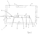
- a hermetically sealed package 2 comprises a housing 4 having a base 6 and an upright side wall 8 surrounding the base 6 to define an open chamber 10.
- a platform 9 is located within the housing 4 adjacent the base 6 to support an optoelectronic modulator 12, in this example, a Mach-Zehnder modulator.
- a first optical fibre 14 is held adjacent and in alignment with a first side 16 of the modulator 12 by a first saddle 18, the first optical fibre 14 leaving the chamber 10 via a first aperture 20 in a first side 22 of the side wall 8.
- a first gas-proof seal 24 is located within the first aperture 20 to permit the first optical fibre 14 to pass through the first aperture 20 whilst maintaining a gas-proof seal between the first aperture 20 and the first optical fibre 14.
- a lens 26 is disposed adjacent a second side 28 of the modulator 12 for focusing electromagnetic radiation onto the second side 28 from a semiconductor laser 29 adjacent the lens 26.
- the optoelectronic modulator 12 is a Pacific Wave Communications, LLC modulator sold under the product code PM-1.5-40-201. However, it should be appreciated that any suitable modulator can be used.
- a lid 30 comprises an oxygen getter 32, formed, in this example, from iron oxide and is attached to the lid 30 which closes the open chamber 10, the lid 30 being seam welded to a top outer periphery of the side wall 8 so as to create a hermetic seal within the chamber 10.
- the chamber 10 also comprises an atmosphere.
- the atmosphere is an inert gas, but any suitable gas, other than oxygen, that does not react chemically with the modulator 12 or any such oxygen sensitive material, preferably having a high atomic mass, can be used, such as Nitrogen.
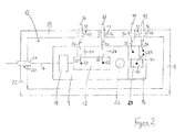
- the modulator 12 comprises a first terminal 48 coupled to a first bond pad 50 via a first bond wire 52.
- the first bond pad 50 is coupled to a first electrical connector 54 via a second bond wire 56, the first electrical connector 54 passing through a second gas-proof seal 60 located within a second aperture 58 in a second side 59 of the side wall 8.
- a second terminal 62 of the modulator 12 is coupled to a second bond pad 64 via a third bond wire 66.
- the second bond pad 64 is coupled to a second electrical connector 68 via a fourth bond wire 70, the second electrical connector 68 passing through a third gas-proof seal 74 located within a third aperture 72 in the second side 59 of the side wall 8.
- the first and second terminals 48, 62 of the modulator 12 are used to provide modulating electrical signals to the modulator 12.
- the laser 29 has a first terminal (not shown) bonded to a third bond pad 76, the third bond pad 76 being coupled to a third electrical connector 78 via a fifth bond wire 80.
- the third electrical connector 78 passes through a fourth gas-proof seal 84 located within a fourth aperture 82 in the second side 59 of the side wall 8.
- a second terminal 86 of the laser 29 is coupled to a fourth bond pad 88 via a sixth bond wire 90, the fourth bond pad 88 being electrically insulated from the third bond pad 76.
- the fourth bond pad 88 is coupled to a fourth electrical connector 92 via a seventh bond wire 94, the fourth electrical connector 92 passing through a fifth gas-proof seal 98 located in a fourth aperture 96 in the second side 59 of the side wall 8.
- the first, second, third and fourth electrical connectors 54, 68, 78, 92 are provided in order to provide electrical signals to the modulator 12 and the laser 29.
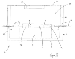
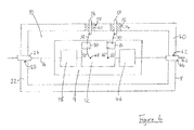
- the package 2 comprises the housing 4 as already described above.
- the chamber 10 comprises the platform 9, the modulator 12, the first saddle 18, the first optical fibre 14, the first aperture 20, the first gas-proof seal 24, the lid 30 and the oxygen getter 32 as already described above in relation to the first example.
- a third side 40 of the side wall 8 comprises a sixth aperture 42 within which is disposed a sixth gas-proof seal 44 in order to permit a second optical fibre 46 to pass through the third side 40 whilst maintaining a gas-proof seal between the sixth aperture 42 and the second optical fibre 46.
- the second optical fibre 46 is held adjacent the second side 28 of the modulator 12 by a second saddle 46.
- the housing 4 does not contain, in this example, the lens 26 and the laser 29, the third bond pad 76, the fifth bond wire 80, the third electrical terminal 78, the fourth gas-proof seal 84, the fourth aperture 82, the sixth bond wire 90, the fourth bond pad 88, the seventh bond wire 94, the fourth electrical connector 92, the fifth gas-proof seal 98 and the fifth aperture 96 are not provided.
- the package 2 can be coupled, in line, between a pair of optical fibres, such as lens fibres, or between an external semiconductor laser (not shown) and an optical fibre by means of coupling to the first and second optical fibres 14, 46, respectively. It should be appreciated that other coupling configurations are envisaged and it is not intended to limit the invention to the above described coupling configurations.
- the housing 4 is initially provided, without the lid 30 and the oxygen getter 32, and the first or second set of parts and components are disposed and anchored within the housing 4 (step 50) depending upon whether construction of the package 4 is required in accordance with to the first example ( Figure 1) or the second example ( Figure 2).
- the oxygen getter 32 is then attached (step 52) to the lid 30.
- the lid 30 with the oxygen getter 32 attached thereto is then placed (step 54) within an oven at a specified temperature, for example 300°C, and for a specified period of time, for example one hour, in order to activate the oxygen getter 32.
- the lid 30 and the getter 32 are then allowed to cool (step 56) before attaching (step 58) the lid 30 with the getter 32 to the housing 4.
- the container is then hermetically sealed (step 60) by seam welding the lid 30 to the housing 4 to close the open chamber 10.
- the above process of attaching the lid 30 to the housing 4 is carried out in a Nitrogen atmosphere and so the atmosphere within the chamber 10 is Nitrogen.
- the package 2 is then leak tested using any suitable technique known in the art.
- the oxygen getter 32 serves to remove any oxygen entering the housing 4 as a result of a failing seal.
- Oxygen molecules entering the housing 4 chemically reacts with the oxygen getter 32 formed from iron oxide in accordance with the following chemical reaction: 4FeO +O 2 ⁇ 2Fe 2 O 3 .
- the present invention is applicable to the packaging of any oxygen sensitive material, for example a polymer material, such as a plastic material.
Landscapes
- Optical Modulation, Optical Deflection, Nonlinear Optics, Optical Demodulation, Optical Logic Elements (AREA)
- Optical Couplings Of Light Guides (AREA)
Abstract
Description
- The present invention relates to a package for an optoelectronic device, the package being of the type used to store oxygen sensitive materials, for example an oxygen sensitive plastic material, such as an optoelectronic modulator formed from the plastic material, in a protective atmosphere, the protective atmosphere being substantially oxygen-free. The present invention also relates to a method of removing oxygen from the protective atmosphere of the above package.
- A package for an optoelectronic modulator comprises a housing having the modulator mounted on an optical platform within the housing. In order to maintain stability of the modulator and prolong the life of the modulator, it is known to avoid the presence of oxygen within the housing. Consequently, the housing is filled with any gas that does not react with or 'poison' the modulator, the gas preferably having a high atomic mass, for example Nitrogen, Zeon or Argon. By filling the housing with the inert gas, the housing comprises an oxygen-free atmosphere. The oxygen-free atmosphere is maintained by hermetically sealing the housing. However, the hermetic seal of the housing can fail leading to ingress of oxygen into the housing, thereby contaminating the oxygen-free atmosphere.
- In contrast with the practice of avoiding the presence of oxygen in the atmosphere within the housing, US 5, 392, 305, US 5, 629, 952 and US 5, 770, 473 disclose the positive presence of oxygen in controlled amounts in the atmosphere within the housing in order to provide stable, long term, continuous operation of a high-power semiconductor laser. In addition to the provision of oxygen, the above documents disclose the use of a getter to control the amount of impurities (excluding oxygen) within the atmosphere of the housing, such as organic impurities.
- According to a first aspect of the present invention, there is provided a package for an optoelectronic device comprising a housing having a substantially oxygen-free gaseous atmosphere hermetically sealed therein, an oxygen-sensitive material located within the housing, and means within the housing for removing oxygen from the gaseous atmosphere so as to prevent oxygen contamination of the gaseous atmosphere in the event of failure of the hermetic seal of the housing.
- Preferably, the means for removing oxygen from the gaseous atmosphere is an oxygen getter.
- Preferably, the oxygen sensitive material is chemically reactive with oxygen in the presence of electromagnetic energy.
- Preferably, the oxygen sensitive material is a polymer material. More preferably, the oxygen sensitive material is a plastic material. Very preferably, the package comprises an optical modulator comprising the oxygen-sensitive material.
- Preferably, the substantially oxygen-free gaseous atmosphere comprises an inert gas.
- Preferably, the package comprises a laser device located within the housing.
- In a preferred embodiment of the invention, there is provided a package for a communications transceiver comprising a housing having: a substantially oxygen-free gaseous atmosphere hermetically sealed therein, a port formed within a wall of the housing for sealingly permitting passage of an optical fibre therethrough into the housing, a clamp for aligning the optical fibre with a plastic modulator located within the housing, a semiconductor laser for launching electromagnetic energy into the plastic modulator, and a lens located between the semiconductor laser and the plastic modulator, the housing being characterised by an oxygen getter located therein for removing oxygen from the gaseous atmosphere so as to prevent oxygen contamination of the gaseous atmosphere in the event of failure of the hermetic seal of the housing.
- According to a second aspect of the present invention, there is provided a transceiver device comprising the package as set forth above in relation to the first aspect of the present invention.
- According to a third aspect of the present invention, there is provided a method of preventing oxygen ingress into a housing for an optoelectronic device package, the housing comprising a substantially oxygen-free gaseous atmosphere hermetically sealed therein and an oxygen-sensitive material located within the housing, the method comprising the step of: providing means within the housing for removing oxygen from the gaseous atmosphere so as to prevent oxygen contamination of the gaseous atmosphere in the event of failure of the hermetic seal of the housing.
- Preferably, the step of providing the means for removing oxygen from the gaseous atmosphere comprises providing an oxygen getter.
- At least one embodiment of the invention will now be described, by way of example only, with reference to the accompanying drawing, in which:
- Figure 1 is a schematic diagram of a package constituting a first embodiment of the present invention;
- Figure 2 is a plan view of the package of Figure 1 without a lid;
- Figure 3 is a schematic diagram of a package constituting a second embodiment of the present invention;
- Figure 4 is a plan view of the package of Figure 3 without a lid, and
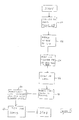
- Figure 5 is a flow diagram of a method of fabricating the packages of Figurel and/or Figure 3.
-
- Throughout the following description identical reference numerals will be used to identify like parts.
- In a first example of the invention (Figure 1), a hermetically sealed
package 2 comprises ahousing 4 having a base 6 and anupright side wall 8 surrounding the base 6 to define anopen chamber 10. Aplatform 9 is located within thehousing 4 adjacent the base 6 to support anoptoelectronic modulator 12, in this example, a Mach-Zehnder modulator. A firstoptical fibre 14 is held adjacent and in alignment with afirst side 16 of themodulator 12 by afirst saddle 18, the firstoptical fibre 14 leaving thechamber 10 via afirst aperture 20 in afirst side 22 of theside wall 8. In this respect, a first gas-proof seal 24 is located within thefirst aperture 20 to permit the firstoptical fibre 14 to pass through thefirst aperture 20 whilst maintaining a gas-proof seal between thefirst aperture 20 and the firstoptical fibre 14. - A
lens 26 is disposed adjacent asecond side 28 of themodulator 12 for focusing electromagnetic radiation onto thesecond side 28 from asemiconductor laser 29 adjacent thelens 26. In this example, theoptoelectronic modulator 12 is a Pacific Wave Communications, LLC modulator sold under the product code PM-1.5-40-201. However, it should be appreciated that any suitable modulator can be used. - A
lid 30 comprises anoxygen getter 32, formed, in this example, from iron oxide and is attached to thelid 30 which closes theopen chamber 10, thelid 30 being seam welded to a top outer periphery of theside wall 8 so as to create a hermetic seal within thechamber 10. Thechamber 10 also comprises an atmosphere. In this example, the atmosphere is an inert gas, but any suitable gas, other than oxygen, that does not react chemically with themodulator 12 or any such oxygen sensitive material, preferably having a high atomic mass, can be used, such as Nitrogen. - Referring to Figure 2, the
modulator 12 comprises afirst terminal 48 coupled to afirst bond pad 50 via afirst bond wire 52. Thefirst bond pad 50 is coupled to a firstelectrical connector 54 via asecond bond wire 56, the firstelectrical connector 54 passing through a second gas-proof seal 60 located within asecond aperture 58 in a second side 59 of theside wall 8. Asecond terminal 62 of themodulator 12 is coupled to asecond bond pad 64 via athird bond wire 66. Thesecond bond pad 64 is coupled to a secondelectrical connector 68 via afourth bond wire 70, the secondelectrical connector 68 passing through a third gas-proof seal 74 located within athird aperture 72 in the second side 59 of theside wall 8. The first andsecond terminals modulator 12 are used to provide modulating electrical signals to themodulator 12. - The
laser 29 has a first terminal (not shown) bonded to athird bond pad 76, thethird bond pad 76 being coupled to a thirdelectrical connector 78 via a fifth bond wire 80. The thirdelectrical connector 78 passes through a fourth gas-proof seal 84 located within a fourth aperture 82 in the second side 59 of theside wall 8. Asecond terminal 86 of thelaser 29 is coupled to a fourth bond pad 88 via asixth bond wire 90, the fourth bond pad 88 being electrically insulated from thethird bond pad 76. The fourth bond pad 88 is coupled to a fourthelectrical connector 92 via a seventh bond wire 94, the fourthelectrical connector 92 passing through a fifth gas-proof seal 98 located in a fourth aperture 96 in the second side 59 of theside wall 8. - The first, second, third and fourth
electrical connectors modulator 12 and thelaser 29. - In this example, the above described parts and components constitute a first set of parts and components.
- Referring to Figures 3 and 4, in a second example, the
package 2 comprises thehousing 4 as already described above. Within thehousing 4, thechamber 10 comprises theplatform 9, themodulator 12, thefirst saddle 18, the firstoptical fibre 14, thefirst aperture 20, the first gas-proof seal 24, thelid 30 and the oxygen getter 32 as already described above in relation to the first example. In addition, instead of thelens 12 and thelaser 14, athird side 40 of theside wall 8 comprises asixth aperture 42 within which is disposed a sixth gas-proof seal 44 in order to permit a secondoptical fibre 46 to pass through thethird side 40 whilst maintaining a gas-proof seal between thesixth aperture 42 and the secondoptical fibre 46. The secondoptical fibre 46 is held adjacent thesecond side 28 of themodulator 12 by asecond saddle 46. Since thehousing 4 does not contain, in this example, thelens 26 and thelaser 29, thethird bond pad 76, the fifth bond wire 80, the thirdelectrical terminal 78, the fourth gas-proof seal 84, the fourth aperture 82, thesixth bond wire 90, the fourth bond pad 88, the seventh bond wire 94, the fourthelectrical connector 92, the fifth gas-proof seal 98 and the fifth aperture 96 are not provided. - In this example, the parts and components described above in connection with this second example constitute a second set of parts and components.
- The
package 2 can be coupled, in line, between a pair of optical fibres, such as lens fibres, or between an external semiconductor laser (not shown) and an optical fibre by means of coupling to the first and secondoptical fibres - Assembly of the
package 2 of Figures 1 and 3 will now be described with reference to Figure 5. It should be noted that while this is the preferred method of construction it is not exclusively limited to the process described. - The
housing 4 is initially provided, without thelid 30 and the oxygen getter 32, and the first or second set of parts and components are disposed and anchored within the housing 4 (step 50) depending upon whether construction of thepackage 4 is required in accordance with to the first example (Figure 1) or the second example (Figure 2). - The oxygen getter 32 is then attached (step 52) to the
lid 30. Thelid 30 with the oxygen getter 32 attached thereto is then placed (step 54) within an oven at a specified temperature, for example 300°C, and for a specified period of time, for example one hour, in order to activate theoxygen getter 32. Thelid 30 and thegetter 32 are then allowed to cool (step 56) before attaching (step 58) thelid 30 with thegetter 32 to thehousing 4. The container is then hermetically sealed (step 60) by seam welding thelid 30 to thehousing 4 to close theopen chamber 10. The above process of attaching thelid 30 to thehousing 4 is carried out in a Nitrogen atmosphere and so the atmosphere within thechamber 10 is Nitrogen. Thepackage 2 is then leak tested using any suitable technique known in the art. - Since the sealing of the
package 2 is likely to fail over a period of years, theoxygen getter 32 serves to remove any oxygen entering thehousing 4 as a result of a failing seal. Oxygen molecules entering thehousing 4 chemically reacts with theoxygen getter 32 formed from iron oxide in accordance with the following chemical reaction: 4FeO +O2→ 2Fe2O3. - Although the above examples have been described in the context of the
package 2 containing the oxygensensitive modulator 12, it should be appreciated that the present invention is applicable to the packaging of any oxygen sensitive material, for example a polymer material, such as a plastic material.
Claims (11)
- A package for an optoelectronic device comprising a housing having a substantially oxygen-free gaseous atmosphere hermetically sealed therein, an oxygen-sensitive material located within the housing, and means for removing oxygen from the gaseous atmosphere so as to prevent oxygen contamination of the gaseous atmosphere in the event of failure of the hermetic seal of the housing.
- A package as claimed in Claim 1, wherein the means for removing oxygen from the gaseous atmosphere is an oxygen getter.
- A package as claimed in Claim 1 or Claim 2, wherein the oxygen sensitive material is chemically reactive with oxygen in the presence of electromagnetic energy.
- A package as claimed in any one of the preceding claims, wherein the oxygen sensitive material is a polymer material.
- A package as claimed in any one of the preceding claims, wherein the oxygen sensitive material is a plastic material.
- A package as claimed in any one of the preceding claims, further comprising an optical modulator comprising the oxygen-sensitive material.
- A package as claimed in any one of the preceding claims, wherein the substantially oxygen-free gaseous atmosphere comprises a gas that does not react with the oxygen-sensitive material.
- A package as claimed in any one of the preceding claims, further comprising a laser device located within the housing.
- A transceiver device comprising the package as claimed in any one of the preceding claims.
- A method of preventing oxygen ingress into a housing for an optoelectronic device package, the housing comprising a substantially oxygen-free gaseous atmosphere hermetically sealed therein and an oxygen-sensitive material located within the housing, the method comprising the step of:providing means for removing oxygen from the gaseous atmosphere so as to prevent oxygen contamination of the gaseous atmosphere in the event of failure of the hermetic seal of the housing.
- A method as claimed in Claim 10, wherein the step of providing the means for removing oxygen from the gaseous atmosphere comprises providing an oxygen getter.
Priority Applications (1)
| Application Number | Priority Date | Filing Date | Title |
|---|---|---|---|
| EP01304660A EP1261037A1 (en) | 2001-05-25 | 2001-05-25 | Package for optoelectronic device and method therefor |
Applications Claiming Priority (1)
| Application Number | Priority Date | Filing Date | Title |
|---|---|---|---|
| EP01304660A EP1261037A1 (en) | 2001-05-25 | 2001-05-25 | Package for optoelectronic device and method therefor |
Publications (1)
| Publication Number | Publication Date |
|---|---|
| EP1261037A1 true EP1261037A1 (en) | 2002-11-27 |
Family
ID=8181986
Family Applications (1)
| Application Number | Title | Priority Date | Filing Date |
|---|---|---|---|
| EP01304660A Withdrawn EP1261037A1 (en) | 2001-05-25 | 2001-05-25 | Package for optoelectronic device and method therefor |
Country Status (1)
| Country | Link |
|---|---|
| EP (1) | EP1261037A1 (en) |
Cited By (2)
| Publication number | Priority date | Publication date | Assignee | Title |
|---|---|---|---|---|
| WO2004010498A3 (en) * | 2002-07-24 | 2004-12-02 | Johnson Matthey Plc | Oxygen getter and method for forming it |
| US8829634B2 (en) | 2009-03-23 | 2014-09-09 | Dow Global Technologies Llc | Optoelectronic device |
Citations (4)
| Publication number | Priority date | Publication date | Assignee | Title |
|---|---|---|---|---|
| JPH05343812A (en) * | 1992-06-12 | 1993-12-24 | Kubota Corp | Semiconductor device |
| JPH07335777A (en) * | 1994-06-13 | 1995-12-22 | Toshiba Corp | Optical semiconductor device |
| WO1999035681A1 (en) * | 1998-01-07 | 1999-07-15 | Fed Corporation | Assembly for and method of packaging integrated display devices |
| US6121577A (en) * | 1997-12-20 | 2000-09-19 | Daimlerchrysler Ag | Electrically heatable glow plug with oxygen getter material |
-
2001
- 2001-05-25 EP EP01304660A patent/EP1261037A1/en not_active Withdrawn
Patent Citations (4)
| Publication number | Priority date | Publication date | Assignee | Title |
|---|---|---|---|---|
| JPH05343812A (en) * | 1992-06-12 | 1993-12-24 | Kubota Corp | Semiconductor device |
| JPH07335777A (en) * | 1994-06-13 | 1995-12-22 | Toshiba Corp | Optical semiconductor device |
| US6121577A (en) * | 1997-12-20 | 2000-09-19 | Daimlerchrysler Ag | Electrically heatable glow plug with oxygen getter material |
| WO1999035681A1 (en) * | 1998-01-07 | 1999-07-15 | Fed Corporation | Assembly for and method of packaging integrated display devices |
Non-Patent Citations (2)
| Title |
|---|
| PATENT ABSTRACTS OF JAPAN vol. 018, no. 174 (E - 1530) 24 March 1994 (1994-03-24) * |
| PATENT ABSTRACTS OF JAPAN vol. 1996, no. 04 30 April 1996 (1996-04-30) * |
Cited By (2)
| Publication number | Priority date | Publication date | Assignee | Title |
|---|---|---|---|---|
| WO2004010498A3 (en) * | 2002-07-24 | 2004-12-02 | Johnson Matthey Plc | Oxygen getter and method for forming it |
| US8829634B2 (en) | 2009-03-23 | 2014-09-09 | Dow Global Technologies Llc | Optoelectronic device |
Similar Documents
| Publication | Publication Date | Title |
|---|---|---|
| US7348203B2 (en) | Hermetic packaging | |
| KR100298149B1 (en) | Packaged high power semiconductor lasers and methods of manufacturing the same | |
| US5805757A (en) | Apparatus and method for preserving optical characteristics of a fiber optic device | |
| EP1093162A1 (en) | Hermatic firewall for mems packaging in flip-chip bonded geometry | |
| EP2028521A1 (en) | Packaging for an Interferometric Modulator | |
| US20050095749A1 (en) | Device for protecting a chip and method for operating a chip | |
| JP2006524417A (en) | Sealed glass package and manufacturing method thereof | |
| KR102403432B1 (en) | A thermal mass flow sensor, a method for manufacturing the thermal mass flow sensor, and a thermal mass flow meter using the thermal mass flow sensor | |
| JPWO2002054548A1 (en) | Short wavelength laser module and manufacturing method thereof | |
| EP1499560B1 (en) | Device for protecting a chip and method for operating a chip | |
| CN109781659B (en) | Preparation method of photoelectric detector with reference air chamber | |
| US20030021311A1 (en) | Semiconductor laser module, optical measuring method and optical measuring apparatus | |
| JP4629843B2 (en) | Semiconductor laser module and manufacturing method and system thereof | |
| US4913986A (en) | Battery fill-post seal arrangement for hermeticity leakage testing | |
| JP2005250307A (en) | Optical deflector | |
| US6161688A (en) | Arrangement of at least one of electrical components and optical components in a gas-tight packaging and method for manufacturing the same | |
| US8395177B2 (en) | Package for protecting a device from ambient substances | |
| US5680495A (en) | Fiber optic device sealed by compressed metal seals and method for making the same | |
| Nagata et al. | Mechanical reliability of LiNbO3optical modulators hermetically sealed in stainless steel packages | |
| CN223742796U (en) | Butterfly-shaped optical device for vacuum environment | |
| JP3017922B2 (en) | Gas filling method for sodium-sulfur battery container | |
| US3060656A (en) | Manufacture of hermetically sealed semiconductor device | |
| JPS594187A (en) | Airtight sealing of gaas | |
| CN109585701A (en) | A kind of packaging tool and packaging method | |
| CA2356978A1 (en) | Sealed container for optical components and sealed feedthrough for optical fibres |
Legal Events
| Date | Code | Title | Description |
|---|---|---|---|
| PUAI | Public reference made under article 153(3) epc to a published international application that has entered the european phase |
Free format text: ORIGINAL CODE: 0009012 |
|
| AK | Designated contracting states |
Kind code of ref document: A1 Designated state(s): AT BE CH CY DE DK ES FI FR GB GR IE IT LI LU MC NL PT SE TR |
|
| AX | Request for extension of the european patent |
Free format text: AL;LT;LV;MK;RO;SI |
|
| 17P | Request for examination filed |
Effective date: 20030527 |
|
| AKX | Designation fees paid |
Designated state(s): DE FR GB |
|
| 17Q | First examination report despatched |
Effective date: 20061002 |
|
| RAP1 | Party data changed (applicant data changed or rights of an application transferred) |
Owner name: AGILENT TECHNOLOGIES, INC. |
|
| STAA | Information on the status of an ep patent application or granted ep patent |
Free format text: STATUS: THE APPLICATION IS DEEMED TO BE WITHDRAWN |
|
| 18D | Application deemed to be withdrawn |
Effective date: 20070213 |