EP1260847A2 - Optical element, scanning optical system having the same, and image forming apparatus - Google Patents
Optical element, scanning optical system having the same, and image forming apparatus Download PDFInfo
- Publication number
- EP1260847A2 EP1260847A2 EP02253613A EP02253613A EP1260847A2 EP 1260847 A2 EP1260847 A2 EP 1260847A2 EP 02253613 A EP02253613 A EP 02253613A EP 02253613 A EP02253613 A EP 02253613A EP 1260847 A2 EP1260847 A2 EP 1260847A2
- Authority
- EP
- European Patent Office
- Prior art keywords
- scanning
- lattice
- optical
- microstructure
- light beam
- Prior art date
- Legal status (The legal status is an assumption and is not a legal conclusion. Google has not performed a legal analysis and makes no representation as to the accuracy of the status listed.)
- Granted
Links
Images


Classifications
-
- G—PHYSICS
- G02—OPTICS
- G02B—OPTICAL ELEMENTS, SYSTEMS OR APPARATUS
- G02B26/00—Optical devices or arrangements for the control of light using movable or deformable optical elements
- G02B26/08—Optical devices or arrangements for the control of light using movable or deformable optical elements for controlling the direction of light
- G02B26/10—Scanning systems
-
- G—PHYSICS
- G02—OPTICS
- G02B—OPTICAL ELEMENTS, SYSTEMS OR APPARATUS
- G02B26/00—Optical devices or arrangements for the control of light using movable or deformable optical elements
- G02B26/08—Optical devices or arrangements for the control of light using movable or deformable optical elements for controlling the direction of light
- G02B26/10—Scanning systems
- G02B26/12—Scanning systems using multifaceted mirrors
- G02B26/124—Details of the optical system between the light source and the polygonal mirror
Definitions
- the present invention relates to an optical element which exhibits a change in incidence angle and a scanning optical system having the optical element.
- the present invention is suitable for an image forming apparatus such as a laser beam printer or digital copying apparatus which has, for example, an electrophotographic process of deflecting a light beam emitted from a light source means by using a light deflector (deflecting means), and recording image information by optically scanning a scanning target surface through a scanning optical means including an optical element having f- ⁇ characteristics and a microstructure lattice formed thereon.
- a light beam which is optically modulated in accordance with an image signal and emitted from a light source means is cyclically deflected by a light deflector formed from, e.g., a polygon mirror, and the light beam is focused into a spot on the surface of a photosensitive recording medium and optically scanned by an imaging optical system having f- ⁇ characteristics.
- a light deflector formed from, e.g., a polygon mirror
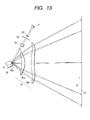
- Fig. 13 is a sectional view (main scanning cross-section) of a conventional scanning optical system in the main scanning direction.
- a light source means 91 is formed from, for example, a semiconductor laser or the like.
- a collimator lens 92 converts a divergent light beam emitted from the light source means 91 into an almost parallel light beam.
- An aperture stop 93 shapes a beam shape by limiting a light beam that passes through.
- a cylindrical lens 94 has a predetermined power in only the sub-scanning direction and forms a light beam which passes through the aperture stop 93 into an almost line image on a deflecting surface (reflecting surface) 95a of a light deflector 95 (to be described later) within a sub-scanning cross-section.
- the light deflector 95 serving as a deflecting means is formed from, for example, a polygon mirror (rotating polyhedral mirror) having a tetrahedral arrangement.
- the light deflector 95 is rotated by a driving means (not shown) such as a motor at constant speed in the direction indicated by an arrow A in Fig. 13.
- a scanning lens system 96 serves as a scanning optical means having a focusing function and f- ⁇ characteristics and is formed from first and second scanning lenses 96a and 96b.
- the scanning lens system 96 forms the light beam based on image information, which is reflected/deflected by the light deflector 95, into an image on a photosensitive drum surface 97 serving as a scanning target surface, and has an optical face tangle error correction function of making the deflecting surface 95a of the light deflector 95 and the photosensitive drum surface 97 have a conjugate relationship within a sub-scanning cross-section.
- the divergent light beam emitted from the semiconductor laser 91 is converted into an almost parallel light beam by the collimator lens 92, and the light beam (light amount) is limited by the aperture stop 93.
- the resultant light beam is incident on the cylindrical lens 94.
- the substantially parallel light beam incident on the cylindrical lens 94 the light in a main scanning cross-section emerges without any change.
- the light in a sub-scanning cross-section is focused and substantially formed into a line image (elongated in the main scanning direction) on the deflecting surface 95a of the light deflector 95.
- the light beam reflected/deflected by the deflecting surface 95a of the light deflector 95 is formed into a spot on the photosensitive drum surface 97 via the first and second scanning lenses 96a and 96b.
- This light beam is then scanned on the photosensitive drum surface 97 at constant speed in the direction indicated by an arrow B (main scanning direction) by rotating the light deflector 95 in the direction indicated by the arrow A. With this operation, an image is recorded on the photosensitive drum surface 97 as a recording medium.
- the scanning optical means (scanning lens system) of a scanning optical system is generally made of a plastic material that allows easy formation of an aspherical shape and is easy to manufacture. It is, however, difficult in terms of technique and cost to form an antireflection coat on the lens surface of a plastic lens. As a consequence, Fresnel reflection occurs on each optical surface.
- the first problem is therefore that surface reflected light on a lens surface without an antireflection coat is reflected by other optical surfaces and finally reaches a scanning target surface to produce ghosts. If one of the two scanning lenses which is closer to the light deflector has a concave lens surface and a light beam incident thereon is nearly vertical, Fresnel reflected light on this lens surface returns to the light deflector and reflected by the deflecting surface (reflecting surface) of the light deflector. This reflected light passes through the scanning optical means and reaches the scanning target surface to become a ghost.
- the second problem is that since the incidence angle of a light beam incident on the scanning optical means generally changes as it travels from an on-axis position (scanning center) to an off-axis position (scanning periphery), Fresnel reflection on each optical surface greatly changes to produce a difference between the light amount at an on-axis position and that at an off-axis position.
- Fig. 15 is a graph showing a transmission on each surface when P-polarized light beam is incident on the scanning optical means in Fig. 13. As shown in Fig. 14, since the reflectance decreases (transmission increases) with an increase in incidence angle, the transmission of the overall system increases from an on-axis position to an off-axis position. That is, the illuminance distribution on the scanning target surface also increases from an on-axis position to an off-axis position.
- the light amount at the outermost off-axis position is larger than that at an on-axis position by 5%.
- the image output from the image forming apparatus has a density difference between a central portion and a peripheral portion.
- a lattice is formed at a desired pitch with a desired power distribution to realize magnification chromatic aberration correction or focus correction, and the lattice height (depth) of the diffraction grating surface is properly set to change the diffraction efficiency of diffracted light (1st-order diffracted light) to be used at an on-axis position and an off-axis position, thereby canceling out a change in transmission on other refracting surfaces.
- diffracted light of another order increases.
- the increased diffracted light of another order reaches the scanning target surface to become flare light to cause image deterioration unless the light is shielded by using a light-shielding wall or the like.
- Further object of the present invention is to provide an optical element having a microstructure lattice formed on at least one optical surface, wherein the microstructure lattice is formed from an arrangement for collecting a change in an amount of light transmitted which is caused as an incidence angle of a light beam changes from a central portion to a peripheral portion.
- the microstructure lattice is a zero-order lattice.
- the optical surface is a lens surface, diffracting surface, or mirror surface, and comprises a flat or curved surface.
- the microstructure lattice is integrally formed with a substrate on which the optical surface is formed.
- the arrangement for collecting the change in the amount of light transmitted is based on at least one of a lattice pitch, lattice depth, and lattice constant of the microstructure lattice.
- a material for the microstructure lattice is a transparent resin or glass material.
- Further object of the present invention is to provide a scanning optical system for deflecting a light beam emitted from light source means by using deflecting means, guiding the light beam deflected by the deflecting means onto a scanning surface by using scanning optical means, and scanning the scanning surface
- the scanning optical means includes an optical element having a microstructure lattice formed on at least one optical surface, and the microstructure lattice is formed from an arrangement for collecting a change in an amount of light transmitted which is caused as an incidence angle of a light beam incident on the optical element from an on-axis position to an off-axis position.
- the optical surface on which the microstructure lattice is formed is a surface, of optical surfaces of the scanning optical means, which exhibits a largest change in incidence angle due to a field angle.
- the microstructure lattice is configured such that a direction of change in the total amount of light transmitted changing from a scanning center of an optical surface on which the microstructure lattice is provided to a scanning periphery is opposite to a direction of change in the total amount of light transmitted changing from a scanning center of an optical surface on which the microstructure lattice is not provided to a scanning periphery.
- the microstructure lattice is formed on all optical surfaces of the scanning optical means.
- the microstructure lattice is a zero-order lattice.
- each optical surface other than the surface on which the microstructure lattice is formed is formed from a refracting surface or/and a reflecting surface, and the change in the total amount of light beam transmitted the scanning optical means is based on a transmission produced when an incidence angle of a light beam changes from a scanning center to a scanning periphery on the refracting surface or/and a reflectance produced when an incidence angle of a light beam changes from a scanning center to a scanning periphery on the reflecting surface.
- ⁇ be a scanning angle
- Id( ⁇ ) be the total amount of light transmitted through the microstructure lattice at the scanning angle ⁇
- It( ⁇ ) be the total amount of light transmitted, at the scanning angle ⁇ , through an optical surface other than the optical surface on which the microstructure lattice is formed
- Further object of the present invention is to provide a scanning optical system for deflecting a light beam emitted from light source means by using deflecting means, guiding the light beam deflected by the deflecting means onto a scanning surface by using scanning optical means, and scanning the scanning surface
- the scanning optical means includes an optical element having a microstructure lattice formed on at least one optical surface, and Py ⁇ ⁇ /(Ns + Ni ⁇ sin ⁇ i) is satisfied, where Py is a lattice pitch at a position y from a center at which a light beam reaching a predetermined image height on the scanning surface passes through the microstructure lattice, ⁇ is a wavelength of a light beam from the light source means, ⁇ i is an incidence angle of a light beam at the position y, Ni is a refractive index of a medium on an incident side of the microstructure lattice, and Ns is a refractive index of a medium on an exit side of the microstructure lattice.
- At least one of a lattice pitch, lattice depth, and lattice constant is determined for the microstructure lattice in accordance with an incidence angle at a position where a light beam reaching a predetermined image height passes through the microstructure lattice.
- Pymax be a lattice pitch determined when a maximum incidence angle of a light beam incident on the microstructure lattice is set to ⁇ ymax, the microstructure lattice is formed at a pitch P given by P ⁇ Pymax.
- At least one of a lattice pitch, lattice depth, and lattice constant is changed at a scanning center and a scanning periphery on the microstructure lattice in accordance with an incidence angle at a position where a light beam reaching a predetermined image height passes through the microstructure lattice.
- the optical surface on which the microstructure lattice is formed is a surface, of optical surfaces of the scanning optical means, which exhibits a largest change in incidence angle due to a field angle.
- the microstructure lattice is configured such that a direction of change in the total amount of light transmitted changing from a scanning center of an optical surface on which the microstructure lattice is provided to a scanning periphery is opposite to a direction of change in the total amount of light transmitted changing from a scanning center of an optical surface on which the microstructure lattice is not provided to a scanning periphery.
- the microstructure lattice is formed on all optical surfaces of the scanning optical means.
- the microstructure lattice is formed on an optical surface which is a spherical surface, aspherical surface, rotational asymmetrical curved surface, or diffracting surface.
- the microstructure lattice is formed on a flat optical surface.
- a material for the microstructure lattice is a transparent resin or glass material.
- an image forming apparatus comprising any one of above mentioned the scanning optical system, a photosensitive member placed on the scanning surface, a developing device which develops an electrostatic latent image, formed on the photosensitive member by a light beam scanned by the scanning optical system, as a toner image, a transferring device which transfers the developed toner image onto a transfer material, and a fixing deice which fixes the transferred toner image onto the transfer material.
- Further object of the present invention is to provide an image forming apparatus comprising any one of above mentioned scanning optical system, and a printer controller which converts code data input from an external device into an image signal, and inputs the image signal to the scanning optical. system.
- the incidence angle of the light beam to be incident to the microstructure lattice is set ⁇ and an amount of light transmitted on the microstructure lattice surface is set Is( ⁇ ), 0.9 ⁇ Is( ⁇ )/Is(0) ⁇ 1.1 is satisfied.
- An optical element according to the present invention is an optical element having a microstructure lattice formed on at least one optical surface.
- the microstructure lattice is designed to adjust a change in the amount of light transmitted which is caused as the incidence angle of a light beam changes from the central portion to the peripheral portion.
- the optical element of the present invention can be applied to various optical systems, e.g., a photographing system, projection system, and image forming system, in which the incidence angle changes from the central portion to the peripheral portion of the element.
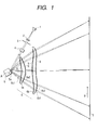
- Fig. 1 is a sectional view (main scanning sectional view) of the main part of the scanning optical system in the main scanning direction according to the first embodiment of the present invention.
- the direction in which a light beam is reflected/deflected (deflected/scanned) by a deflecting means is defined as a main scanning direction
- a direction perpendicular to the optical axis of the scanning optical means and the main scanning direction is defined as a sub-scanning direction.
- a light source means 1 is formed from, for example, a semiconductor laser.
- a collimator lens 2 converts the divergent light beam emitted from the light source means 1 into a substantially parallel light beam.
- An aperture stop 3 limits a light beam that passes therethrough and shapes it into a beam shape.
- a cylindrical lens 4 has a predetermined power only in the sub-scanning direction and forms the light beam having passed through the aperture stop 3 into an almost line image on a deflecting surface (reflecting surface) 5a of a light deflector 5 (to be described later) within a sub-scanning cross-section.
- the light deflector 5 serves as a deflecting means and is formed from, for example, a polygon mirror (rotating polyhedral mirror) having a tetrahedral arrangement.
- the light deflector 5 is rotated by a driving means (not shown) such as a motor at constant speed in the direction indicated by an arrow A in Fig. 1.
- a scanning lens system 6 serves as a scanning optical means having a focusing function and f- ⁇ characteristics and is formed from first and second scanning lenses 6a and 6b made of a plastic material.
- the scanning lens system 6 forms the light beam based on image information, which is reflected/deflected by the light deflector 5, into an image on a photosensitive drum surface 7 serving as a scanning target surface, and has an optical face tangle error correction function of making the deflecting surface 5a of the light deflector 5 and the photosensitive drum surface 7 have a conjugate relationship within a sub-scanning cross-section.
- a light beam from the light source means 1 may be directly incident on the light deflector 5 without using the optical elements 2, 3, and 4 described above.
- Each of the lens surfaces of the first and second scanning lenses 6a and 6b in this embodiment has a curved surface, i.e., a spherical or aspherical surface within the main scanning cross-section shown in Fig. 1, and also has a known special aspherical surface as a base shape whose curvature changes from an on-axis position (scanning center) to an off-axis position (scanning periphery) within a sub-scanning cross-section perpendicular to the main scanning cross-section.
- microstructure lattices 8 made of a transparent resin or glass material (to be described later) are entirely formed on an incident surface 6a1 and exit surface 6a2 of the first scanning lens 6a and an incident surface 6b1 and exit surface 6b2 of the second scanning lens 6b.
- the divergent light beam emitted from the semiconductor laser 1 is converted into a substantially parallel light beam by the collimator lens 2.
- This light beam (light amount) is then limited by the aperture stop 3 and incident on the cylindrical lens 4.
- the substantially parallel light beam incident on the cylindrical lens 4 the light in a main scanning cross-section emerges without any change.
- the light in a sub-scanning cross-section is focused and substantially formed into a line image (elongated in the main scanning direction) on the deflecting surface 5a of the light deflector 5.
- the light beam reflected/deflected by the deflecting surface 5a of the light deflector 5 is formed into a spot on the photosensitive drum surface 7 via the first and second scanning lenses 6a and 6b.
- This light beam is then scanned on the photosensitive drum surface 7 at constant speed in the direction indicated by an arrow B (main scanning direction) by rotating the light deflector 5 in the direction indicated by the arrow A. With this operation, an image is recorded on the photosensitive drum surface 7 as a recording medium.
- the semiconductor laser 1 serving as a light source is so positioned as to cause light to be incident as almost P-polarized light on the scanning lens system 6. That is, the semiconductor laser 1 is so positioned as to make its transverse mode almost parallel to the photosensitive drum surface 7.
- the incident surface 6a1 and exit surface 6a2 of the first scanning lens 6a and the incident surface 6b1 and exit surface 6b2 of the second scanning lens 6b of the scanning optical means 6 have special aspherical surface shapes as base shapes.
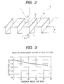
- the microstructure lattice 8 shown in Fig. 2 is entirely formed on each of these surfaces. This makes it possible to arbitrarily control transmission and properly adjust the illuminance distribution on the scanning target surface 7.
- the microstructure lattice 8 may be formed on a given one optical surface (having the highest incidence angle dependency) that most influences the illuminance distribution on the scanning target surface 7.
- one or a plurality of microstructure lattices 8 may be formed to make the illuminance distribution on the scanning target surface 7 uniform.
- the microstructure lattice 8 may be formed on a spherical surface, aspherical surface, rotational asymmetrical curved surface, diffracting surface, mirror surface, or flat surface.
- the microstructure lattice 8 has a repetitive structure in which pairs of lattice portions 81 and non-lattice portions 82 are arrayed in the one-dimensional direction (main scanning direction).
- Letting P be a lattice pitch equal to a length of one period of the lattice portion 81 and non-lattice portion 82, and F be a lattice constant, a length L of the lattice portion 81 in the array direction is given by L F x P.
- D the depth of the lattice.
- the microstructure lattice 8 may be integrally formed with a substrate (glass substrate or transparent resin substrate) on which an optical surface is formed.
- a lattice pitch P that satisfies a condition for a so-called zero-order lattice is selected.
- the microstructure lattice 8 is called SWS (subwave structure), which has a lattice pitch 1/10 to 1/100 that of a general diffraction grating and is designed to be used for zeroth-order light having no diffracting effect.
- a zero-order lattice is a lattice that produces no diffracted light other than zeroth-order light in a periodic microstructure lattice (see Optical Society of America Vol. 11, No. 10/October 1994/J. Opt. Soc. Am. A, p. 2965).
- diffracted light is generally produced at a diffraction angle that satisfies the following conditional expression for diffraction:
- P(Ns ⁇ sin ⁇ m - Ni ⁇ sin ⁇ i) m ⁇ ...(1)
- P is the lattice pitch
- Ni is the refractive index (of the medium of the microstructure lattice) on the incident side
- ⁇ i is the incidence angle
- ⁇ m is the m-order diffraction angle
- Ns is the refractive index (of the medium of the microstructure lattice) on the light incidence side
- m is the diffraction order
- ⁇ is the operating wavelength.
- ⁇ be the wavelength of the light beam from the light source means 1
- ⁇ i be the incidence angle of the light beam at the position y
- Ni be the refractive index of the medium of the microstructure lattice 8 on the incident side
- Ns be the refractive index of the medium of the microstructure lattice 8 on the exit side
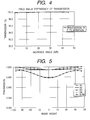
- This graph shows the maximum pitch that satisfies the condition for a zero-order lattice; no diffracted light other than zeroth-order light is produced below this pitch. It is obvious from this graph that if the lattice pitch P of the microstructure lattice is 0.5 ⁇ m when the incidence angle ⁇ i is zero, i.e., in the case of normal incidence, the lattice behaves as a zero-order lattice.
- the condition for a zero-order lattice is not satisfied when the lattice pitch P of the microstructure lattice is 0.5 ⁇ m.
- the lattice pitch P for a zero-order lattice must be smaller than 0.35 ⁇ m.
- the incidence angle ⁇ i of an incident light beam is determined at the position y on each lens surface of the scanning lens system 6, i.e., the incident surface 6a1 and exit surface 6a2 of the first scanning lens 6a and the incident surface 6b1 and exit surface 6b2 of the second scanning lens 6b. Therefore, the maximum pitch that satisfies the condition for a zero-order lattice can be determined at each position on each lens surface.
- the microstructure lattice 8 may be formed at the lattice pitch P given by P ⁇ Pymax
- a pitch equal to or smaller than Pymax may be set as the lattice pitch P.
- a microstructure lattice is formed such that the lattice array direction coincides with the polarization direction of a light beam, i.e., each groove of the lattice becomes perpendicular to the polarization direction of a light beam.
- the polarization direction of a light beam coincides with P polarization (a direction parallel to the drawing surface of Fig. 1).
- the lattice array direction may be made parallel or perpendicular to the polarization direction of a light beam.
- the microstructure lattice is optimized to reduce a change in the transmission of P polarization of zeroth-order light regardless of the incidence angle.
- Fig. 4 shows the transmission characteristic of P polarization with respect to the incidence angle with this lattice shape.
- This microstructure lattice 8 is formed on each optical surface, i.e., the incident surface 6a1 and exit surface 6a2 of the first scanning lens 6a and the incident surface 6b1 and exit surface 6b2 of the second scanning lens 6b.
- Fig. 5 shows the transmission of each optical surface and the transmission of the overall system in this arrangement.
- the microstructure lattice 8 formed on each optical surface of the scanning lens means 6 can greatly reduce a change in the amount of light transmitted which is caused as the incidence angle changes from an on-axis position (scanning center) to an off-axis position (scanning periphery). This makes it possible to reduce a change in the total amount of light transmitted in the overall scanning lens means 6 and make the illuminance distribution on the scanning target surface 7 almost uniform.
- a lattice pitch, lattice depth, and lattice constant are determined in accordance with the incidence angle at a position where a light beam reaching a predetermined image height passes through so as to reduce the difference between the amount of light transmitted at an on-axis position (scanning center) and that at an off-axis position (scanning periphery) on each optical surface.
- each of the lens surfaces of the first and second scanning lenses 6a and 6b has a spherical or aspherical surface within a main scanning cross-section, and also has a known special aspherical surface as a base shape whose curvature changes from an on-axis position to an off-axis position within a sub-scanning cross-section.
- the present invention is not limited to this shape as long as each lens is a so-called f- ⁇ lens having a function (f- ⁇ characteristics) of forming a polarized light beam into a spot on the scanning target surface 7 and scanning it at constant speed.
- the light source means 1 is formed from a single-beam laser.
- the present invention is not limited to this.
- a composite multi-beam light source may be used, which is formed by combining the optical paths of mono-chip multi-beam or single-beam laser having a plurality of light-emitting portions through a beam combining means and the like.
- the semiconductor laser 1 is so positioned as to cause a light beam to be incident as almost P-polarized light on the scanning lens means 6.
- a light beam may be incident as S-polarized light or an arbitrary polarization direction may be set.
- the shape of the microstructure lattice 8 may be optimized in accordance with the polarization direction of a light beam incident on the scanning lens means 6.
- the lattice shape obtained by arraying rectangular cross-sections in a one-dimensional direction has been exemplified.
- the present invention is not limited to this. This shape may be optimized by using triangular, trapezoidal, or wavy cross-sections and arraying them in a two-dimensional direction as well as in a one-dimensional direction.
- a technique of forming the shape of a microstructure lattice in an injection mold and molding a microstructure lattice As a method of forming a microstructure lattice on a lens surface, a technique of forming the shape of a microstructure lattice in an injection mold and molding a microstructure lattice.
- the scanning lens means 6 is comprised of two lenses.
- this means may be formed from a single or three or more lenses.
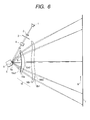
- Fig. 6 is a sectional view (main scanning cross-section) of the main part of the second embodiment of the present invention in the main scanning direction.
- the same reference numerals as in Fig. 1 denote the same parts in Fig. 6.
- This embodiment differs from the first embodiment in that a microstructure lattice 8 is formed on only an incident surface 16a1 of a first lens 16a of a scanning optical means 16.
- Other arrangements and optical effects are the same as those in the first embodiment, and hence the same effects as those of the first embodiment are obtained.
- the scanning lens system 16 serves as a scanning optical means having a focusing function and f- ⁇ characteristics.
- the scanning optical means 16 is formed from two scanning lenses, i.e., first and second lenses 16a and 16b, made of a plastic material.
- the scanning lens means 16 forms the light beam based on image information, which is reflected/deflected by a light deflector 5, into an image on a photosensitive drum surface 7 serving as a scanning target surface, and has an optical face tangle error correction function of making a deflecting surface 5a of the light deflector 5 and the photosensitive drum surface 7 have a conjugate relationship within a sub-scanning cross-section.
- each of the lens surfaces of the first and second scanning lenses 16a and 16b has a curved surface, i.e., a spherical or aspherical surface within a main scanning cross-section in Fig. 6, and also has a known special aspherical surface as a base shape whose curvature changes from an on-axis (scanning center) position to an off-axis position (scanning periphery) within a sub-scanning cross-section.
- the microstructure lattice 8 is formed on only the incident surface 16a1 of the first lens 16a of the scanning optical means 16.
- a lattice constant F is set as follows.
- the incidence angle ⁇ i of a light beam is determined at a position y on the lens surface of the incident surface 16a1 of the first lens 16a of the scanning optical means 16. It suffices if the amount of light transmitted (transmission) through the incident surface 16a1 of the first lens 16a is determined on this result to make the total amount of light transmitted through the scanning optical means 16 at an arbitrary image height almost constant. That is, the lattice constant F may be optimized in correspondence with the incidence angle ⁇ i such that a desired transmission is set at the position y on the incident surface 16a1 of the first lens 16a.
- an optimal transmission can be set by setting different lattice constants F at an on-axis position (scanning center) and off-axis position (scanning periphery) on the microstructure lattice 8 in accordance with the incidence angle at the position where a light beam reaching a predetermined image height passes through the microstructure lattice 8.
- Fig. 8 shows the result obtained by optimization according to the above procedure.
- Fig. 8 shows the transmission of each of optical surfaces including the incident surface 16a1 and exit surface 16a2 of the first lens 16a and the incident surface 16b1 and exit surface 16b2 of the scanning lens 16b and the transmission of the overall system.
- ⁇ be the scanning angle of a deflected light beam corresponding to an arbitrary image height
- Id( ⁇ ) be the amount of light transmitted through the microstructure lattice 8 on the incident surface 16a1 of the first lens 16a of the scanning optical means 16 at the scanning angle ⁇
- It( ⁇ ) be the total amount of light transmitted through the respective optical surfaces other than the surface on which the microstructure lattice 8 is formed, i.e., the exit surface 16a2 of the first lens 16a and the incident surface 16b1 and exit surface 16b2 of the scanning lens 16b at the scanning angle ⁇
- the following inequality is satisfied within the scanning angle: 0.8 ⁇ (Id( ⁇ ) ⁇ It( ⁇ ))/(Id(0) ⁇ It(0)) ⁇ 1.2 ...(6)
- the illuminance distribution on the scanning target surface 7 can be kept almost uniform by making settings such that a change in the amount of light transmitted which is caused as the incidence angle changes from an on-axis position (scanning center) to an off-axis position (scanning periphery) on the microstructure lattice 8 of the scanning optical means 16 cancels out a change in the total amount of light transmitted which is caused as the incidence angle changes from an on-axis position to an off-axis position on each optical surface other than the optical surface on which the microstructure lattice 8 is formed.
- a change in the total amount of light transmitted through the scanning optical means 16 is based on the transmission originating from a change in the incidence angle of a light beam from a scanning center to a scanning periphery on a refracting surface.
- the illuminance distribution on the scanning target surface 7 is made almost uniform by making the field angle characteristic of the antireflection function of the microstructure lattice 8 cancel out the field angle characteristic based on the transmission from an on-axis position to an off-axis position on each optical surface other than the optical surface on which the microstructure lattice 8 is formed.
- the microstructure lattice 8 is set on the incident surface 16a1 of the first lens 16a of the scanning optical means 16.
- a microstructure lattice may be set on another optical surface as in the embodiment described later, or microstructure lattices may be set on a plurality of optical surfaces.
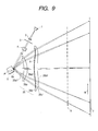
- Fig. 9 is a sectional view (main scanning cross-section) showing the main part of the third embodiment of the present invention in the main scanning direction.
- the same reference numerals as in Fig. 1 denote the same parts in Fig. 9.
- This embodiment differs from the first embodiment in that a microstructure lattice 8 is formed on only an incident surface 26b1 of a second lens 26b of a scanning optical means 26, and an optical path folding mirror 9 is placed between the second lens 26b and a scanning target surface 7.
- Other arrangements and optical effects are the same as those in the first embodiment, and hence the same effects as those of the first embodiment are obtained.
- the scanning lens system 26 serves as a scanning optical means having a focusing function and f- ⁇ characteristics.
- the scanning optical means 26 is formed from two scanning lenses, i.e., first and second lenses 26a and 26b, made of a plastic material.
- the scanning lens means; 16 forms the light beam based on image information, which is reflected/deflected by a light deflector 5, into an image on a photosensitive drum surface 7 serving as a scanning target surface, and has an optical face tangle error correction function of making a deflecting surface 5a of the light deflector 5 and the photosensitive drum surface 7 have a conjugate relationship within a sub-scanning cross-section.
- each of the lens surfaces of the first and second scanning lenses 26a and 26b has a curved surface, i.e., a spherical or aspherical surface within a main scanning cross-section in Fig. 9, and also has a known special aspherical surface as a base shape whose curvature changes from an on-axis (scanning center) position to an off-axis position (scanning periphery) within a sub-scanning cross-section.
- the microstructure lattice 8 is formed on only the incident surface 26b1 of the first lens 26b of the scanning optical means 26.
- a lattice depth D is set as follows.
- the incidence angle ⁇ i of a light beam is determined at a position y on the lens surface of the incident surface 26b1 of the second lens 26b of the scanning optical means 26. It suffices if the amount of light transmitted (transmission) through the incident surface 26b1 of the second lens 26b is determined on this result to make the total amount of light transmitted through the scanning optical means 26 at an arbitrary image height almost constant. That is, the lattice depth D may be optimized in correspondence with the incidence angle ⁇ i such that a desired transmission is set at the position y on the incident surface 26b1 of the second lens 26b.
- an optimal transmission can be set by setting different lattice depths D at an on-axis position (scanning center) and off-axis position (scanning periphery) on the microstructure lattice 8 in accordance with the incidence angle at the position where a light beam reaching a predetermined image height passes through the microstructure lattice 8.
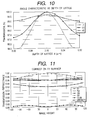
- Fig. 11 shows the result obtained by optimization according to the above procedure.
- Fig. 11 shows the transmission of each of optical surfaces including the incident surface 26a1 and exit surface 26a2 of the first lens 26a and the incident surface 26b1 and exit surface 26b2 of the scanning lens 26b, the reflectance of the optical surface of the optical path folding mirror 9, and the transmission of the overall system.
- ⁇ be the scanning angle of a deflected light beam corresponding to an arbitrary image height
- Id( ⁇ ) be the amount of light transmitted through the microstructure lattice 8 on the incident surface 26b1 of the second lens 26b of the scanning optical means 26 at the scanning angle ⁇
- It( ⁇ ) be the total amount of light transmitted at the scanning angle ⁇ , which is calculated from the transmissions of the respective optical surfaces other than the surface on which the microstructure lattice 8 is formed, i.e., the incident surface 26a1 and exit surface 26a2 of the first lens 26a and the exit surface 26b2 of the second lens 26b and the reflectance of the reflecting surface of the optical path folding mirror 9, the following inequality is satisfied within the scanning angle: 0.8 ⁇ (Id( ⁇ ) ⁇ It( ⁇ ))/(Id(0) ⁇ It(0)) ⁇ 1.2 ...(6)
- the illuminance distribution on the scanning target surface 7 can be kept almost uniform by making settings such that a change in the amount of light transmitted which is caused as the incidence angle changes from an on-axis position (scanning center) to an off-axis-position (scanning periphery) on the microstructure lattice 8 of the scanning optical means 26 cancels out a change in the total amount of light transmitted which is caused as the incidence angle changes from an on-axis position to an off-axis position on each optical surface other than the optical surface on which the microstructure lattice 8 is formed.
- a change in the total amount of light beam transmitted through the scanning optical means 26 originates from a change in transmission which is caused as the incidence angle of a light beam changes from a scanning center to a scanning periphery on a refracting surface and a change in reflectance which is caused by a change in the incidence angle of a light beam from a scanning center to a scanning periphery on a reflecting surface.
- microstructure lattice 8 is set on the incident surface 26b1 of the second lens 26b of the scanning optical means 26.
- a microstructure lattice may be set on the optical surface of an optical path folding mirror having a plane diffracting or reflecting surface, or microstructure lattices may be set on a plurality of optical surfaces.
- the transmission is optimized by setting different lattice constants F or lattice depths D at an on-axis position (scanning center) and an off-axis position (scanning periphery) on the microstructure lattice 8 in accordance with the incidence angle at the position where a light beam reaching a predetermined image height passes through the microstructure lattice 8.
- the present invention is not limited to this.
- different lattice pitches P, lattice depths D, and lattice constants F may be set altogether.
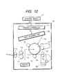
- Fig. 12 is a sectional view showing the main part of an image forming apparatus (electrophotographic printer) in a sub-scanning cross-section, which uses the scanning optical system according to the first, second, or third embodiment described above.
- an image forming apparatus 104 receives code data Dc from an external device 117 such as a personal computer. This code data Dc is converted into image data (dot data) Di by the printer controller 111 in the apparatus.
- the image data Di is input to an optical scanning unit 100 having the arrangement exemplified by each of the first, second, and third embodiments.
- a light beam 103 modulated in accordance with the image data Di emerges from the optical scanning unit (scanning optical system) 100.
- the photosensitive surface of a photosensitive drum 101 is scanned with this light beam 103 in the main scanning direction.
- the photosensitive drum 101 serving as an electrostatic latent image bearing member is rotated clockwise by a motor 115. With this rotation, the photosensitive surface of the photosensitive drum 101 moves in the sub-scanning direction perpendicular to the main scanning direction.
- a charge roller 102 is placed above the surface of the photosensitive drum 101 to be in contact with its surface so as to uniformly charge it.
- the surface of the photosensitive drum 101 charged by the charge roller 102 is irradiated with the light beam 103 scanned by the optical scanning unit 100.
- the light beam 103 is modulated on the basis of the image data Di.
- an electrostatic latent image is formed on the surface.
- This electrostatic latent image is developed into a toner image by a developing device 107 placed downstream from the irradiation position of the light beam 103 within a rotating cross-section of the photosensitive drum 101 so as to be in contact with the photosensitive drum 101.
- the toner image developed by the developing device 107 is transferred onto a paper sheet 112 serving as a transfer member by a transferring roller (transferring device) 108.
- the paper sheet 112 is stored in a paper cassette 109 in front of the photosensitive drum 101 (on the right side in Fig. 12). However, a paper sheet can also be fed manually.
- a pickup roller 110 is placed at an end portion of the paper cassette 109 to feed the paper sheet 112 from the paper cassette 109 into a convey path.
- the paper sheet 112 on which the unfixed toner image is transferred is conveyed to a fixing device behind the photosensitive drum 101 (on the left side in Fig. 12).
- the fixing device is constituted by a fixing roller 113 incorporating a fixing heater (not shown) and a press roller 114 placed in contact with the fixing roller 113.
- the fixing device fixes the unfixed toner image on the paper sheet 112 by heating the paper sheet 112 conveyed from the transferring unit while pressing it between the fixing roller 113 and the press portion of the press roller 114.
- the image-fixed paper sheet 112 is discharged from the image forming apparatus by using a sheet discharging roller 116 placed behind the fixing roller 113.
- the printer controller 111 controls the respective units in the image forming apparatus including the motor 115 and the polygon motor in the optical scanning unit 100 as well as the data conversion described above.
- the optical element having the microstructure lattice designed to adjust a change in the amount of light transmitted which is caused as the incidence angle of a light beam changes from the central portion to the peripheral portion is applied to the scanning optical system to implement an optical element which can easily adjust the amount of light transmitted which is caused as the incidence angle of a light beam changes and a scanning optical system having the optical element.
- an optical element which can make the light amount distribution on the scanning target surface uniform by reducing Fresnel reflection on the lens surface which causes flare or ghost without increasing a step such as a coating step, and an optical system having the optical element can be implemented.
- an optical element which can make the illuminance distribution almost uniform in a wide area on an image surface and an optical system using the optical element can be implemented.
Landscapes
- Physics & Mathematics (AREA)
- General Physics & Mathematics (AREA)
- Optics & Photonics (AREA)
- Facsimile Scanning Arrangements (AREA)
- Mechanical Optical Scanning Systems (AREA)
- Lenses (AREA)
- Diffracting Gratings Or Hologram Optical Elements (AREA)
- Facsimile Heads (AREA)
Abstract
Description
Fig. 8 shows the transmission of each of optical surfaces including the incident surface 16a1 and exit surface 16a2 of the
This code data Dc is converted into image data (dot data) Di by the
Claims (29)
- An optical element having a microstructure lattice formed on at least one optical surface, characterized in that
said microstructure lattice is formed from an arrangement for collecting a change in an amount of light transmitted which is caused as an incidence angle of a light beam changes from a central portion to a peripheral portion. - An optical element according to claim 1, characterized in that said microstructure lattice is a zero-order lattice.
- An optical element according to claim 1 or 2, characterized in that the optical surface is a lens surface, diffracting surface, or mirror surface, and comprises a flat or curved surface.
- An optical element according to claim 1, 2, or 3, characterized in that said microstructure lattice is integrally formed with a substrate on which the optical surface is formed.
- An optical element according to any one of claims 1 to 4, characterized in that the arrangement for collecting the change in the amount of light transmitted is based on at least one of a lattice pitch, lattice depth, and lattice constant of said microstructure lattice.
- An optical element according to any one of claims 1 to 5, characterized in that a material for said microstructure lattice is a transparent resin or glass material.
- An optical system characterized by comprising said optical element according to any one of claims 1 to 6.
- A scanning optical system for deflecting a light beam emitted from light source means by using deflecting means, guiding the light beam deflected by said deflecting means onto a scanning surface by using scanning optical means, and scanning the scanning surface, characterized in that
said scanning optical means includes an optical element having a microstructure lattice formed on at least one optical surface, and said microstructure lattice is formed from an arrangement for collecting a change in an amount of light transmitted which is caused as an incidence angle of a light beam incident on said optical element from an on-axis position to an off-axis position. - A scanning optical system according to claim 8, characterized in that the optical surface on which said microstructure lattice is formed is a surface, of optical surfaces of said scanning optical means, which exhibits a largest change in incidence angle due to a field angle.
- A scanning optical system according to claim 8, characterized in that said microstructure lattice is configured such that a direction of change in the total amount of light transmitted changing from a scanning center of an optical surface on which said microstructure lattice is provided to a scanning periphery is opposite to a direction of change in the total amount of light transmitted changing from a scanning center of an optical surface on which said microstructure lattice is not provided to a scanning periphery.
- A scanning optical system according to claim 8, characterized in that said microstructure lattice is formed on all optical surfaces of said scanning optical means.
- A scanning optical system according to claim 8, characterized in that said microstructure lattice is a zero-order lattice.
- A scanning optical system according to claim 8, characterized in that each optical surface other than the surface on which said microstructure lattice is formed is formed from a refracting surface or/and a reflecting surface, and the change in the total amount of light beam transmitted said scanning optical means is based on a transmission produced when an incidence angle of a light beam changes from a scanning center to a scanning periphery on the refracting surface or/and a reflectance produced when an incidence angle of a light beam changes from a scanning center to a scanning periphery on the reflecting surface.
- A scanning optical system according to claim 8, characterized in that letting be a scanning angle, Id() be the total amount of light transmitted through said microstructure lattice at the scanning angle , and It() be the total amount of light transmitted, at the scanning angle , through an optical surface other than the optical surface on which said microstructure lattice is formed,
- A scanning optical system for deflecting a light beam emitted from light source means by using deflecting means, guiding the light beam deflected by said deflecting means onto a scanning surface by using scanning optical system, and scanning the scanning surface, characterized in that
said scanning optical means includes an optical element having a microstructure lattice formed on at least one optical surface, and - A scanning optical system according to claim 15, characterized in that in order to reduce a light amount difference between a scanning center and a scanning periphery on a scanning surface, at least one of a lattice pitch, lattice depth, and lattice constant is determined for said microstructure lattice in accordance with an incidence angle at a position where a light beam reaching a predetermined image height passes through said microstructure lattice.
- A scanning optical system according to claim 15, characterized in that letting Pymax be a lattice pitch determined when a maximum incidence angle of a light beam incident on said microstructure lattice is set to ymax, said microstructure lattice is formed at a pitch P given by
- A scanning optical system according to claim 15, characterized in that at least one of a lattice pitch, lattice depth, and lattice constant is changed at a scanning center and a scanning periphery on said microstructure lattice in accordance with an incidence angle at a position where a light beam reaching a predetermined image height passes through said microstructure lattice.
- A scanning optical system according to any one of claims 15 to 18, characterized in that the optical surface on which said microstructure lattice is formed is a surface, of optical surfaces of said scanning optical means, which exhibits a largest change in incidence angle due to a field angle.
- A scanning optical system according to any one of claims 15 to 18, characterized in that said microstructure lattice is configured such that a direction of change in the total amount of light transmitted changing from a scanning center of an optical surface on which said microstructure lattice is provided to a scanning periphery is opposite to a direction of change in the total amount of light transmitted changing from a scanning center of an optical surface on which said microstructure lattice is not provided to a scanning periphery.
- A scanning optical system according to any one of claims 15 to 18, characterized in that said microstructure lattice is formed on all optical surfaces of said scanning optical means.
- A scanning optical system according to any one of claims 15 to 21, characterized in that said microstructure lattice is formed on an optical surface which is a spherical surface, aspherical surface, rotational asymmetrical curved surface, or diffracting surface.
- A scanning optical system according to any one of claims 15 to 21, characterized in that said microstructure lattice is formed on a flat optical surface.
- A scanning optical system according to any one of claims 15 to 23, characterized in that a material for said microstructure lattice is a transparent resin or glass material.
- An image forming apparatus characterized by comprising said scanning optical system according to any one of claims 8 to 24, a photosensitive member placed on the scanning surface, a developing device which develops an electrostatic latent image, formed on said photosensitive member by a light beam scanned by said scanning optical system, as a toner image, a transferring device which transfers the developed toner image onto a transfer material, and a fixing deice which fixes the transferred toner image onto the transfer material.
- An image forming apparatus characterized by comprising said scanning optical system according to any one of claims 8 to 24, and a printer controller which converts code data input from an external device into an image signal, and inputs the image signal to said scanning optical system.
- An optical element according to claim 1,
characterized in that, when the incidence angle of the light beam to be incident to said microstructure lattice is set and an amount of light transmitted on said microstructure lattice surface is set Is(), - A scanning optical system according to claim 8, characterized in that, when the incidence angle of the light beam to be incident to said microstructure lattice is set and an amount of light transmitted on said microstructure lattice surface is set Is(),
- A scanning optical system according to claim 15, characterized in that, when the incidence angle of the light beam to be incident to said microstructure lattice is set and an amount of light transmitted on said microstructure lattice surface is set Is(),
Applications Claiming Priority (2)
| Application Number | Priority Date | Filing Date | Title |
|---|---|---|---|
| JP2001157368 | 2001-05-25 | ||
| JP2001157368A JP2002350624A (en) | 2001-05-25 | 2001-05-25 | Optical element, scanning optical system having the same, and image forming apparatus |
Publications (3)
| Publication Number | Publication Date |
|---|---|
| EP1260847A2 true EP1260847A2 (en) | 2002-11-27 |
| EP1260847A3 EP1260847A3 (en) | 2004-01-21 |
| EP1260847B1 EP1260847B1 (en) | 2008-08-06 |
Family
ID=19001245
Family Applications (1)
| Application Number | Title | Priority Date | Filing Date |
|---|---|---|---|
| EP02253613A Expired - Lifetime EP1260847B1 (en) | 2001-05-25 | 2002-05-22 | Scanning optical system with microstructure grating, and image forming apparatus |
Country Status (7)
| Country | Link |
|---|---|
| US (1) | US6927917B2 (en) |
| EP (1) | EP1260847B1 (en) |
| JP (1) | JP2002350624A (en) |
| KR (1) | KR100499880B1 (en) |
| CN (1) | CN1388385A (en) |
| DE (1) | DE60228018D1 (en) |
| ES (1) | ES2307710T3 (en) |
Cited By (5)
| Publication number | Priority date | Publication date | Assignee | Title |
|---|---|---|---|---|
| EP1391771A3 (en) * | 2002-08-08 | 2004-06-16 | Canon Kabushiki Kaisha | Optical scanning device and image forming apparatus using the same |
| EP1507152A1 (en) * | 2003-08-13 | 2005-02-16 | Canon Kabushiki Kaisha | Optical element having minute periodic structure |
| EP1345062A3 (en) * | 2002-03-13 | 2005-03-30 | Canon Kabushiki Kaisha | Scanning optical system and image forming apparatus using the same |
| EP1456696A4 (en) * | 2001-12-17 | 2006-03-01 | Canon Kk | Optical element and scanning optical system having the same, and image forming apparatus |
| EP1643546A3 (en) * | 2004-10-01 | 2009-04-22 | Canon Kabushiki Kaisha | Method for manufacturing a nanostructure |
Families Citing this family (23)
| Publication number | Priority date | Publication date | Assignee | Title |
|---|---|---|---|---|
| JP4393049B2 (en) * | 2002-09-17 | 2010-01-06 | キヤノン株式会社 | Scanning optical system and image forming apparatus using the same |
| JP4593886B2 (en) * | 2003-06-04 | 2010-12-08 | キヤノン株式会社 | Optical scanning device and image forming apparatus using the same |
| US7633033B2 (en) | 2004-01-09 | 2009-12-15 | General Lasertronics Corporation | Color sensing for laser decoating |
| US7268948B2 (en) * | 2004-03-31 | 2007-09-11 | Canon Kabushiki Kaisha | Optical element and optical scanning device using the same |
| WO2007018149A1 (en) * | 2005-08-08 | 2007-02-15 | Matsushita Electric Industrial Co., Ltd. | Imaging optical system |
| WO2007053242A2 (en) * | 2005-09-19 | 2007-05-10 | Wayne State University | Transparent hydrophobic article having self-cleaning and liquid repellant features and method of fabricating same |
| US20090231714A1 (en) * | 2005-09-19 | 2009-09-17 | Yang Zhao | Transparent anti-reflective article and method of fabricating same |
| WO2007142186A1 (en) * | 2006-06-06 | 2007-12-13 | Panasonic Corporation | Optical member |
| US8536483B2 (en) * | 2007-03-22 | 2013-09-17 | General Lasertronics Corporation | Methods for stripping and modifying surfaces with laser-induced ablation |
| WO2009005840A1 (en) * | 2007-07-05 | 2009-01-08 | General Lasertronics Corporation | Aperture adapters for laser-based coating removal end-effector |
| JP5106033B2 (en) * | 2007-10-16 | 2012-12-26 | キヤノン株式会社 | Optical scanning device and image forming apparatus using the same |
| US10112257B1 (en) | 2010-07-09 | 2018-10-30 | General Lasertronics Corporation | Coating ablating apparatus with coating removal detection |
| US8891147B2 (en) * | 2011-05-27 | 2014-11-18 | Hitachi-Lg Data Storage, Inc. | Optical beam scanning device and image display device using the same |
| KR101548445B1 (en) * | 2011-06-22 | 2015-08-28 | 히다치 막셀 가부시키가이샤 | Image display device |
| JP5309234B2 (en) * | 2012-02-27 | 2013-10-09 | 京セラドキュメントソリューションズ株式会社 | Optical scanning device and image forming apparatus using the same |
| US9895771B2 (en) | 2012-02-28 | 2018-02-20 | General Lasertronics Corporation | Laser ablation for the environmentally beneficial removal of surface coatings |
| US10086597B2 (en) | 2014-01-21 | 2018-10-02 | General Lasertronics Corporation | Laser film debonding method |
| CN106486883A (en) * | 2015-08-28 | 2017-03-08 | 高准精密工业股份有限公司 | Light emitting device |
| CN105824125A (en) * | 2016-05-25 | 2016-08-03 | 西安炬光科技股份有限公司 | Method and device for laser beam expanding |
| CN109477961B (en) * | 2016-07-19 | 2021-02-26 | 麦克赛尔株式会社 | Projection type image display device |
| US10527923B2 (en) * | 2018-02-07 | 2020-01-07 | Yazaki Corporation | Scanning projector transmissive screen, and scanning projector system |
| CN112771420B (en) * | 2018-09-28 | 2023-04-14 | 富士胶片株式会社 | Optical elements and light polarizing devices |
| CN111913166B (en) * | 2019-05-10 | 2023-08-18 | 苏州旭创科技有限公司 | Multi-angle light beam expanding system and laser radar |
Family Cites Families (14)
| Publication number | Priority date | Publication date | Assignee | Title |
|---|---|---|---|---|
| JPS58174906A (en) | 1982-04-07 | 1983-10-14 | Ricoh Co Ltd | Method for preventing surface reflection of optical element |
| US5355244A (en) * | 1991-09-18 | 1994-10-11 | Ricoh Company Ltd. | Optical scanner for reducing shading |
| US5208701A (en) * | 1991-12-24 | 1993-05-04 | Xerox Corporation | Wobble correction lens with binary diffractive optic surface and refractive cylindrical surface |
| JPH09500459A (en) | 1994-05-02 | 1997-01-14 | フィリップス エレクトロニクス ネムローゼ フェンノートシャップ | Light transmitting optical element having anti-reflection diffraction grating |
| JPH08146333A (en) * | 1994-11-22 | 1996-06-07 | Minolta Co Ltd | Laser scanning optical device |
| US5838480A (en) * | 1996-04-29 | 1998-11-17 | The University Of Rochester | Optical scanning system with diffractive optics |
| JPH10160906A (en) | 1996-11-29 | 1998-06-19 | Sony Corp | Lens with antireflection film and method of forming antireflection film |
| JP2000075229A (en) * | 1998-09-01 | 2000-03-14 | Canon Inc | Scanning optical system |
| JP2000137109A (en) | 1998-10-30 | 2000-05-16 | Shimadzu Corp | Antireflection device using diffraction grating |
| JP3684094B2 (en) * | 1999-01-19 | 2005-08-17 | ペンタックス株式会社 | Scanning optical system |
| JP3495951B2 (en) * | 1999-05-28 | 2004-02-09 | キヤノン株式会社 | Scanning optical device and image forming apparatus |
| JP4174171B2 (en) * | 1999-06-16 | 2008-10-29 | キヤノン株式会社 | Multi-beam scanning optical system and image forming apparatus using the same |
| JP4266490B2 (en) | 2000-04-25 | 2009-05-20 | キヤノン株式会社 | Scanning optical device and image forming apparatus using the same |
| JP2002182003A (en) | 2000-12-14 | 2002-06-26 | Canon Inc | Anti-reflection function element, optical element, optical system and optical equipment |
-
2001
- 2001-05-25 JP JP2001157368A patent/JP2002350624A/en not_active Withdrawn
-
2002
- 2002-05-20 US US10/147,896 patent/US6927917B2/en not_active Expired - Fee Related
- 2002-05-22 DE DE60228018T patent/DE60228018D1/en not_active Expired - Lifetime
- 2002-05-22 EP EP02253613A patent/EP1260847B1/en not_active Expired - Lifetime
- 2002-05-22 ES ES02253613T patent/ES2307710T3/en not_active Expired - Lifetime
- 2002-05-25 KR KR10-2002-0029127A patent/KR100499880B1/en not_active Expired - Fee Related
- 2002-05-27 CN CN02120653A patent/CN1388385A/en active Pending
Cited By (9)
| Publication number | Priority date | Publication date | Assignee | Title |
|---|---|---|---|---|
| EP1456696A4 (en) * | 2001-12-17 | 2006-03-01 | Canon Kk | Optical element and scanning optical system having the same, and image forming apparatus |
| US7149016B2 (en) | 2001-12-17 | 2006-12-12 | Canon Kabushiki Kaisha | Optical element and scanning optical system having the same and image forming apparatus |
| EP1345062A3 (en) * | 2002-03-13 | 2005-03-30 | Canon Kabushiki Kaisha | Scanning optical system and image forming apparatus using the same |
| EP1391771A3 (en) * | 2002-08-08 | 2004-06-16 | Canon Kabushiki Kaisha | Optical scanning device and image forming apparatus using the same |
| US7034859B2 (en) | 2002-08-08 | 2006-04-25 | Canon Kabushiki Kaisha | Optical scanning device and image forming apparatus using the same |
| US7248279B2 (en) | 2002-08-08 | 2007-07-24 | Canon Kabushiki Kaisha | Optical scanning device and image forming apparatus using the same |
| EP1507152A1 (en) * | 2003-08-13 | 2005-02-16 | Canon Kabushiki Kaisha | Optical element having minute periodic structure |
| US7023630B2 (en) | 2003-08-13 | 2006-04-04 | Canon Kabushiki Kaisha | Optical element having minute periodic structure |
| EP1643546A3 (en) * | 2004-10-01 | 2009-04-22 | Canon Kabushiki Kaisha | Method for manufacturing a nanostructure |
Also Published As
| Publication number | Publication date |
|---|---|
| EP1260847A3 (en) | 2004-01-21 |
| US20020179827A1 (en) | 2002-12-05 |
| CN1388385A (en) | 2003-01-01 |
| KR100499880B1 (en) | 2005-07-07 |
| KR20020090165A (en) | 2002-11-30 |
| US6927917B2 (en) | 2005-08-09 |
| DE60228018D1 (en) | 2008-09-18 |
| ES2307710T3 (en) | 2008-12-01 |
| JP2002350624A (en) | 2002-12-04 |
| EP1260847B1 (en) | 2008-08-06 |
Similar Documents
| Publication | Publication Date | Title |
|---|---|---|
| EP1260847B1 (en) | Scanning optical system with microstructure grating, and image forming apparatus | |
| JP4393049B2 (en) | Scanning optical system and image forming apparatus using the same | |
| JP4454898B2 (en) | Scanning optical system and image forming apparatus having the same | |
| JP3870111B2 (en) | Scanning optical system and image forming apparatus using the same | |
| KR100374276B1 (en) | Optical scanning apparatus and image-forming apparatus using it | |
| JP4617004B2 (en) | Scanning optical device and image forming apparatus using the same | |
| US6424446B2 (en) | Optical scanner and image forming apparatus | |
| JP2000002847A (en) | Scanning optical device and multi-beam scanning optical device | |
| US6639704B2 (en) | Scanning optical apparatus, and image forming apparatus using the same | |
| JP3733294B2 (en) | Scanning optical device and image forming apparatus using the same | |
| JP4817526B2 (en) | Optical scanning device and image forming apparatus using the same | |
| JP4266490B2 (en) | Scanning optical device and image forming apparatus using the same | |
| JP3390118B2 (en) | Optical scanning device, image reading device and image forming device using the same | |
| JP2008116965A (en) | Scanning optical system and image forming apparatus having the same | |
| US20020044357A1 (en) | Imaging element and image reading apparatus | |
| JP2012128085A (en) | Optical scanner and image forming apparatus including the same | |
| JP2025084164A (en) | Optical Scanning Device |
Legal Events
| Date | Code | Title | Description |
|---|---|---|---|
| PUAI | Public reference made under article 153(3) epc to a published international application that has entered the european phase |
Free format text: ORIGINAL CODE: 0009012 |
|
| AK | Designated contracting states |
Kind code of ref document: A2 Designated state(s): AT BE CH CY DE DK ES FI FR GB GR IE IT LI LU MC NL PT SE TR |
|
| AX | Request for extension of the european patent |
Free format text: AL;LT;LV;MK;RO;SI |
|
| PUAL | Search report despatched |
Free format text: ORIGINAL CODE: 0009013 |
|
| AK | Designated contracting states |
Kind code of ref document: A3 Designated state(s): AT BE CH CY DE DK ES FI FR GB GR IE IT LI LU MC NL PT SE TR |
|
| AX | Request for extension of the european patent |
Extension state: AL LT LV MK RO SI |
|
| RIC1 | Information provided on ipc code assigned before grant |
Ipc: 7G 02B 26/12 A Ipc: 7G 02B 1/11 B Ipc: 7G 02B 5/18 B |
|
| 17P | Request for examination filed |
Effective date: 20040611 |
|
| 17Q | First examination report despatched |
Effective date: 20040727 |
|
| AKX | Designation fees paid |
Designated state(s): DE ES FR GB IT NL |
|
| GRAP | Despatch of communication of intention to grant a patent |
Free format text: ORIGINAL CODE: EPIDOSNIGR1 |
|
| RTI1 | Title (correction) |
Free format text: SCANNING OPTICAL SYSTEM WITH MICROSTRUCTURE GRATING, AND IMAGE FORMING APPARATUS |
|
| GRAS | Grant fee paid |
Free format text: ORIGINAL CODE: EPIDOSNIGR3 |
|
| GRAJ | Information related to disapproval of communication of intention to grant by the applicant or resumption of examination proceedings by the epo deleted |
Free format text: ORIGINAL CODE: EPIDOSDIGR1 |
|
| GRAS | Grant fee paid |
Free format text: ORIGINAL CODE: EPIDOSNIGR3 |
|
| 17Q | First examination report despatched |
Effective date: 20040727 |
|
| GRAP | Despatch of communication of intention to grant a patent |
Free format text: ORIGINAL CODE: EPIDOSNIGR1 |
|
| GRAS | Grant fee paid |
Free format text: ORIGINAL CODE: EPIDOSNIGR3 |
|
| GRAA | (expected) grant |
Free format text: ORIGINAL CODE: 0009210 |
|
| AK | Designated contracting states |
Kind code of ref document: B1 Designated state(s): DE ES FR GB IT NL |
|
| REG | Reference to a national code |
Ref country code: GB Ref legal event code: FG4D |
|
| REF | Corresponds to: |
Ref document number: 60228018 Country of ref document: DE Date of ref document: 20080918 Kind code of ref document: P |
|
| REG | Reference to a national code |
Ref country code: ES Ref legal event code: FG2A Ref document number: 2307710 Country of ref document: ES Kind code of ref document: T3 |
|
| PLBE | No opposition filed within time limit |
Free format text: ORIGINAL CODE: 0009261 |
|
| STAA | Information on the status of an ep patent application or granted ep patent |
Free format text: STATUS: NO OPPOSITION FILED WITHIN TIME LIMIT |
|
| 26N | No opposition filed |
Effective date: 20090507 |
|
| PGFP | Annual fee paid to national office [announced via postgrant information from national office to epo] |
Ref country code: NL Payment date: 20120516 Year of fee payment: 11 Ref country code: DE Payment date: 20120531 Year of fee payment: 11 |
|
| PGFP | Annual fee paid to national office [announced via postgrant information from national office to epo] |
Ref country code: GB Payment date: 20120517 Year of fee payment: 11 Ref country code: FR Payment date: 20120620 Year of fee payment: 11 |
|
| PGFP | Annual fee paid to national office [announced via postgrant information from national office to epo] |
Ref country code: IT Payment date: 20120514 Year of fee payment: 11 |
|
| PGFP | Annual fee paid to national office [announced via postgrant information from national office to epo] |
Ref country code: ES Payment date: 20120503 Year of fee payment: 11 |
|
| REG | Reference to a national code |
Ref country code: NL Ref legal event code: V1 Effective date: 20131201 |
|
| GBPC | Gb: european patent ceased through non-payment of renewal fee |
Effective date: 20130522 |
|
| PG25 | Lapsed in a contracting state [announced via postgrant information from national office to epo] |
Ref country code: DE Free format text: LAPSE BECAUSE OF NON-PAYMENT OF DUE FEES Effective date: 20131203 |
|
| PG25 | Lapsed in a contracting state [announced via postgrant information from national office to epo] |
Ref country code: NL Free format text: LAPSE BECAUSE OF NON-PAYMENT OF DUE FEES Effective date: 20131201 Ref country code: IT Free format text: LAPSE BECAUSE OF NON-PAYMENT OF DUE FEES Effective date: 20130522 |
|
| REG | Reference to a national code |
Ref country code: DE Ref legal event code: R119 Ref document number: 60228018 Country of ref document: DE Effective date: 20131203 |
|
| REG | Reference to a national code |
Ref country code: FR Ref legal event code: ST Effective date: 20140131 |
|
| PG25 | Lapsed in a contracting state [announced via postgrant information from national office to epo] |
Ref country code: GB Free format text: LAPSE BECAUSE OF NON-PAYMENT OF DUE FEES Effective date: 20130522 |
|
| PG25 | Lapsed in a contracting state [announced via postgrant information from national office to epo] |
Ref country code: FR Free format text: LAPSE BECAUSE OF NON-PAYMENT OF DUE FEES Effective date: 20130531 |
|
| REG | Reference to a national code |
Ref country code: ES Ref legal event code: FD2A Effective date: 20140606 |
|
| PG25 | Lapsed in a contracting state [announced via postgrant information from national office to epo] |
Ref country code: ES Free format text: LAPSE BECAUSE OF NON-PAYMENT OF DUE FEES Effective date: 20130523 |