EP1260066B1 - Interconnection link redundancy in a modular switch node - Google Patents
Interconnection link redundancy in a modular switch node Download PDFInfo
- Publication number
- EP1260066B1 EP1260066B1 EP01906482A EP01906482A EP1260066B1 EP 1260066 B1 EP1260066 B1 EP 1260066B1 EP 01906482 A EP01906482 A EP 01906482A EP 01906482 A EP01906482 A EP 01906482A EP 1260066 B1 EP1260066 B1 EP 1260066B1
- Authority
- EP
- European Patent Office
- Prior art keywords
- link
- switch
- links
- routing
- data packets
- Prior art date
- Legal status (The legal status is an assumption and is not a legal conclusion. Google has not performed a legal analysis and makes no representation as to the accuracy of the status listed.)
- Expired - Lifetime
Links
- 238000000034 method Methods 0.000 claims description 9
- 238000004891 communication Methods 0.000 claims description 7
- 230000000903 blocking effect Effects 0.000 claims 2
- 238000013519 translation Methods 0.000 description 8
- 230000014616 translation Effects 0.000 description 8
- 230000009977 dual effect Effects 0.000 description 5
- 230000008859 change Effects 0.000 description 3
- 238000010586 diagram Methods 0.000 description 3
- 238000012545 processing Methods 0.000 description 3
- 230000008901 benefit Effects 0.000 description 2
- 230000005540 biological transmission Effects 0.000 description 2
- 238000001514 detection method Methods 0.000 description 2
- 230000003993 interaction Effects 0.000 description 2
- 230000008569 process Effects 0.000 description 2
- 238000012360 testing method Methods 0.000 description 2
- 230000009471 action Effects 0.000 description 1
- 238000013461 design Methods 0.000 description 1
- 238000012986 modification Methods 0.000 description 1
- 230000004048 modification Effects 0.000 description 1
Images



Classifications
-
- H—ELECTRICITY
- H04—ELECTRIC COMMUNICATION TECHNIQUE
- H04L—TRANSMISSION OF DIGITAL INFORMATION, e.g. TELEGRAPHIC COMMUNICATION
- H04L49/00—Packet switching elements
- H04L49/30—Peripheral units, e.g. input or output ports
- H04L49/3081—ATM peripheral units, e.g. policing, insertion or extraction
- H04L49/309—Header conversion, routing tables or routing tags
-
- H—ELECTRICITY
- H04—ELECTRIC COMMUNICATION TECHNIQUE
- H04L—TRANSMISSION OF DIGITAL INFORMATION, e.g. TELEGRAPHIC COMMUNICATION
- H04L49/00—Packet switching elements
- H04L49/15—Interconnection of switching modules
- H04L49/1553—Interconnection of ATM switching modules, e.g. ATM switching fabrics
-
- H—ELECTRICITY
- H04—ELECTRIC COMMUNICATION TECHNIQUE
- H04L—TRANSMISSION OF DIGITAL INFORMATION, e.g. TELEGRAPHIC COMMUNICATION
- H04L49/00—Packet switching elements
- H04L49/25—Routing or path finding in a switch fabric
- H04L49/256—Routing or path finding in ATM switching fabrics
-
- H—ELECTRICITY
- H04—ELECTRIC COMMUNICATION TECHNIQUE
- H04L—TRANSMISSION OF DIGITAL INFORMATION, e.g. TELEGRAPHIC COMMUNICATION
- H04L49/00—Packet switching elements
- H04L49/55—Prevention, detection or correction of errors
- H04L49/552—Prevention, detection or correction of errors by ensuring the integrity of packets received through redundant connections
-
- H—ELECTRICITY
- H04—ELECTRIC COMMUNICATION TECHNIQUE
- H04L—TRANSMISSION OF DIGITAL INFORMATION, e.g. TELEGRAPHIC COMMUNICATION
- H04L12/00—Data switching networks
- H04L12/54—Store-and-forward switching systems
- H04L12/56—Packet switching systems
- H04L12/5601—Transfer mode dependent, e.g. ATM
- H04L2012/5625—Operations, administration and maintenance [OAM]
- H04L2012/5627—Fault tolerance and recovery
-
- H—ELECTRICITY
- H04—ELECTRIC COMMUNICATION TECHNIQUE
- H04L—TRANSMISSION OF DIGITAL INFORMATION, e.g. TELEGRAPHIC COMMUNICATION
- H04L49/00—Packet switching elements
- H04L49/15—Interconnection of switching modules
- H04L49/1515—Non-blocking multistage, e.g. Clos
- H04L49/1523—Parallel switch fabric planes
-
- H—ELECTRICITY
- H04—ELECTRIC COMMUNICATION TECHNIQUE
- H04L—TRANSMISSION OF DIGITAL INFORMATION, e.g. TELEGRAPHIC COMMUNICATION
- H04L49/00—Packet switching elements
- H04L49/25—Routing or path finding in a switch fabric
Definitions
- This invention relates to ATM switches, and more particularly to interconnection link redundancy within an ATM node.
- ATM based telecommunications networks are arranged with a number of ATM switch nodes communicating with one another.
- a design and structure of switch nodes are well known and may take a variety of different forms.
- the physical structure for the node may (and likely will) exceed one physical switch module of boards (for example, one rack).
- the physical infrastructure for the node is often based on several physical switch modules, each containing a number of boards.
- the modules communicate with one another via internal links such that the entire system of modules acts as a single cohesive node unit.
- the reliability of the interconnection links between the several modules in such a large node is crucial. If any link fails between the number of modules, the entire operation of the node is jeopardized. Accordingly, physical redundancy in the interconnection links between modules within a node is preferable.
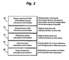
- switch node is viewed as a number of layers ranging from, in the example of Figure 2, power distribution in the bottom layer 28 up to network layer routing and/or connection termination functions with application processing in the upper layer 20.
- the problem commonly associated with the prior art is that the upper layers (20) that run an application are involved in a changeover process from one interconnection link to another (at layer 22). Redundancy operations at layer 22 should occur independently, as much as possible, of the operations of the application in layer 20. If possible, redundancy changeovers at layer 22 should have no or very small interaction with other layers in Figure 2.
- the present invention isolates the interconnection link redundancy layer by means of specific methods for re-routing of traffic flows, either packets or cells, from a failed first interconnection link to another redundant such link between interconnected switch modules, without any involvement of functions in the higher layer.
- a state condition is determined as to "which one within a pair of switch module interconnection links is the primary link over which the packet flow on the connection shall be routed.
- a corresponding routing tag is then attached to each packet on the node-internal connection. If the state of the selected interconnection links changes to a non-operational state, the packet routing will be changed by means of changing the translation of the routing tag within the interconnection link layer so that the packets will be forwarded via the secondary link.”
- interconnection link redundancy is obtained with minimal interaction to the application layer.
- FIG. 1 illustrates an example embodiment of the telecommunications system, within which the present invention may be employed.
- Telecommunications system 10 includes a number of switch nodes A-E communicating with each other through various communication paths.
- Switch nodes A, B, D, and E provide access points for external devices and networks, such as LAN hub 16, PBX 18, Internet 12, host 20, wireless telecommunications network 14, etc.
- external devices and networks such as LAN hub 16, PBX 18, Internet 12, host 20, wireless telecommunications network 14, etc.
- the present invention could be employed in any one of the switch nodes A-E of Figure 1.
- switch node A for example, increases in size (meaning that its capacity to handle data from LAN hub 16, PBX 18, or new external devices increases)
- the physical structure of switch node A will begin to exceed the practical capacity of a physical rack.
- the switch node A is typically divided into two modules communicating with each other. Together, the two modules then comprise the switch node A. Further division can also be envisioned (and frequently occurs) such that one switch node may comprise a number of switch modules communicating one with the others via internal switch node links.
- switch node 30 includes switch module 31 and switch module 32.
- Switch module 31 includes a certain number of device boards (DEV1, DEV2... DEVn) 35 communicating with a switch core 36. The device boards are for application processing and/or node external interfaces.
- On the other end of the switch core 36 is a link termination board (LTa1) 37 communicating with Link A 33.
- Link 33 is a switch module interconnection link in accordance with the present invention. Since switch module 31 and switch module 32 must communicate with each other in order to coherently form together the switch node, it is imperative that link 33 be secure. For that reason, a second link 34 (link R) is provided between switch module 31 and switch module 32 to guarantee operation in the event Link 33 fails.
- link termination board 38 is included within switch module 31 to communicate with switch core 36.
- switch module 32 includes link termination board 39, redundant link termination board 40, switch core 41, and a number of device boards DEV1, DEV2...DEVn 42.
- the present invention is sometimes described herein will reference to "cell" processing, but the invention applies equally well to data packets of variable lengths and to any other data unit switched by the switch core provided the node-internal routing of the data unit over the interconnection links is controlled by a routing tag which can be modified as described.
- Each switch module 31 and 32 can be viewed in terms of its layering, as shown in Figure 2.
- the lowest layer of switch module 31 is power distribution 28. Moving up from the power distribution layer 28, one would find, in order, clock functions 26, ATM switch planes 24, interconnection links 22, and network layer routing and termination devices 20.
- each of the layers 20-28 includes its own redundancy which is as independent as possible from other layers.
- power distribution layer 28 is redundancy terminated (e.g., via diodes), if possible with supervision. Redundancy operations for layer 28 will detect a faulty timer unit or clock reference and will change the unit or reference source when needed. For layer 24, the redundancy operation detects a faulty switch plane and redirects devices to another plane.
- the redundancy termination of the interconnection links is as described in the present invention herein. Specifically, layer 22 redundancy operates to detect a faulty link and re-direct devices to another link. As described above, ideally the network layer routing and termination devices redundancy terminations should be independent of the layers 22-28, to the greatest extent possible.
- each layer should be as orthogonal as possible to all others.
- power distribution to a module is fed via the switch boards that also interconnect exchange terminals, then a redundancy termination relationship exists that must be handled properly in the system.
- the present invention focuses primarily on the interconnection link redundancy at layer 22.
- the present invention re-routes data flow between the switch modules via the alternative physical connection link. Routine testing running in the background over the links 33 and 34 can also be used in addition to the traditional STM/SDH level alarms to discover all link faults, although such routine testing will result in a longer fault period before discovery than the traditional STM/SDH level alarms.
- a switch module such as switch module 31 ( Figure 3) is shown composed of device boards 35 communicating with switch core 36 to link terminations 37 and 38.
- the connection When a connection is set up, the connection is configured as normal on the device boards 35 using, for example, data packet routing tag "a" when Link A 33 is intended for use (in normal circumstances).
- the connection is configured on both of the link terminations 37 and 38 with the same switch segment VCI and the same link segment VPI/VCI.
- the link terminations 37 and 38 include Switch Port Interface Modules (SPIM) communicating with the switch core 36.
- SPIM Switch Port Interface Module
- ATM lay er modules ALM communicate with line termination modules LTM, which provide data packets streams to the respective links 33 and 34.
- the switch port interface modules SPIM of the link termination boards 37 and 38 are informed of all changes in the current link 33 or 34 being used. That is, in normal operation, link A33 may be the current link of choice, such that both SPIMs of link termination 37 and link termination 38 know that all data packets will run between switch modules 31 and 32 via link 33.
- link 33 fails, the dual link state is changed to define the other link 34 as the active link and the SPIMs of the link terminations 37 and 38 and of the device boards 35 are informed of the state change.
- the advantage of the latter embodiment is: by only sending the data packets to the first link A and not to the second link B, the switch core does not need to support multi-cast.
- the support of multi-cast functions in a switch core is in some cases difficult and puts higher requirements on the capacity of the switch since data packets are duplicated.
- the most appropriate position of a routing tag translation table to perform the routing tag addition/translation described above is at the ingress to the switch, i.e., at the "a" close to 35.
- the content of the routing tag translation table at "a" will be changed to redirect the data packets to link B at the detection of a fault in link A. Up until that time no data packets are sent to the link B port, i.e., the SPIM in 38.
- SPIM of link termination board 38 receives and blocks further progress of the data packet, while SPIM of link termination board 37 provides the data packet to the ATM layer module ALM (for ultimate application to link 33).
- link 33 fails, link 34 becomes the active communication link between switch module 31 and 32, such that SPIM 37 no longer applies the data packets from devices 35 to the point a1, while SPIM of link termination board 38 provides the data packets to point a2.
- the switch module is similar to that of Figure 4 except that the "a" tag routing functions are located in the switch core 36' rather than on devices 35. Otherwise elements identified by a "prime” are similarly operating in Figure 4A as described with respect to their counterpart numbers in Figure 4.
- Figures 4 and 4A illustrate that the routing tag translation function can be in the SPIMs or in the switch core.
- the "a" function When operating in the multi-cast mode the "a" function will continuously duplicate the data packets to both the "a1" and the "a2" destinations and the SPIMs on exchange 37' and 38' will either transmit or discard the data packets depending on the active or stand-by state of the links A33' and B34'.
- the devices 35' send data packets with tag "a" and the SPIMs of the link termination boards (in the uni-cast mode) or the "a" re-direction function of the switch core (in the uni-cast mode) determine which of the link A33' or B34' that is used. In either multi-cast or uni-cast mode, to the devices 35', the dual linking operation is essentially invisible.
- the reconfiguration can cause a loss of data packets which have been previously queued on the link termination board handling the faulty link. It is necessary to ensure that the transmission of data packets via the faulty link has definitely ceased before transmission is switched over to the other link, in order to guarantee the data packet sequence order.
- both the first link 33 and the second link 34 by using two different routing tag values with different translations, as long as both links are operational. That is, both of the links 33 and 34 can be operational in a normal mode until a link fault occurs, at which time only one link becomes operational. It is also contemplated in the present invention to implement two independent internal links on the same link termination board (for example 37) by providing the internal links with different data packet routing tags.
- Figures 4 and 4A illustrate the path of data packets from the devices 35 onto the links 33 and/or 34.
- Figure 5 illustrates the flow of data packets from the links 33 and/or 34 to a device 35. Since each connection is configured on both of the link termination boards 37 and 38, data packets arriving from links 33 and/or 34 will automatically be forwarded to the destination device 35 from whichever link they are received. There is thus no need to inform the link termination boards 37 or 38 about the dual link state since the arriving data packets from the links 33 and 34 will be destined for the appropriate device 35 regardless of the link from which they are received. Thus, no specific action is needed after a link fault in order to accommodate data packets being received from the active link into the devices 35.
- a switchover procedure from a first link to a second link must ensure that data packets in the ingress queue from the first link are forwarded to the destination device before data packets on the same user connections arrive via the second link.
- both directions of data packet flow are relocated to another link when a fault is detected in one link, even if the fault is only in one direction.
- the invention is not limited to that
- the set of interconnection links can be considered as a pool of links in which the identity of the active link carrying traffic is of no importance. In other words, once a switch occurs from use of a first link to use of a second link, traffic need not revert back to the first link until (and if) there is a subsequent failure in the second link.
- FIG. 6 illustrates another aspect of an example embodiment of the present invention.
- switch modules 62, 63, 64, and 65 are shown comprising a switch node between user 60 and user 61.
- ATM switching is provided at the end-points, where users 60 and 61 are located. That is, switch module 62 and 65 provide ATM switching. Between switch module 62 and 65, space switching is provided.
Landscapes
- Engineering & Computer Science (AREA)
- Computer Networks & Wireless Communication (AREA)
- Signal Processing (AREA)
- Computer Security & Cryptography (AREA)
- Data Exchanges In Wide-Area Networks (AREA)
Description
- This invention relates to ATM switches, and more particularly to interconnection link redundancy within an ATM node.
- ATM based telecommunications networks are arranged with a number of ATM switch nodes communicating with one another. A design and structure of switch nodes are well known and may take a variety of different forms. As the switch nodes become increasingly large in terms of their capacity to handle data, the physical structure for the node may (and likely will) exceed one physical switch module of boards (for example, one rack). Thus, for many telecommunication nodes, the physical infrastructure for the node is often based on several physical switch modules, each containing a number of boards. The modules communicate with one another via internal links such that the entire system of modules acts as a single cohesive node unit. The reliability of the interconnection links between the several modules in such a large node is crucial. If any link fails between the number of modules, the entire operation of the node is jeopardized. Accordingly, physical redundancy in the interconnection links between modules within a node is preferable.
- A number of methods, as disclosed for example in US-A-5 959 972, for link redundancy are present on the market that require the applications running at the node to closely participate in any changeover process from a first link to a redundant second one. Thus, as shown in Figure 2, switch node is viewed as a number of layers ranging from, in the example of Figure 2, power distribution in the
bottom layer 28 up to network layer routing and/or connection termination functions with application processing in theupper layer 20. The problem commonly associated with the prior art is that the upper layers (20) that run an application are involved in a changeover process from one interconnection link to another (at layer 22). Redundancy operations atlayer 22 should occur independently, as much as possible, of the operations of the application inlayer 20. If possible, redundancy changeovers atlayer 22 should have no or very small interaction with other layers in Figure 2. - The present invention isolates the interconnection link redundancy layer by means of specific methods for re-routing of traffic flows, either packets or cells, from a failed first interconnection link to another redundant such link between interconnected switch modules, without any involvement of functions in the higher layer. When a connection is set up, a state condition is determined as to "which one within a pair of switch module interconnection links is the primary link over which the packet flow on the connection shall be routed. A corresponding routing tag is then attached to each packet on the node-internal connection. If the state of the selected interconnection links changes to a non-operational state, the packet routing will be changed by means of changing the translation of the routing tag within the interconnection link layer so that the packets will be forwarded via the secondary link."
- With the present invention, interconnection link redundancy is obtained with minimal interaction to the application layer.
- These, as well as other objects and advantages of this invention, will be more completely understood and appreciated by careful study of the following more detailed description of a presently preferred exemplary embodiment of the invention taken in conjunction with the accompanying drawings, of which:
-
- FIGURE 1 is a schematic diagram of an example of a telecommunications network;
- FIGURE 2 is a schematic representation of a switch node redundancy layering;
- FIGURE 3 is a schematic diagram of a switch node in accordance with an example embodiment of the present invention;
- FIGURES 4, 4A, and 5 are example embodiments of switch modules in accordance with the present invention; and
- FIGURE 6 is a schematic diagram of various switch modules in accordance with another example embodiment of the present invention.
- Figure 1 illustrates an example embodiment of the telecommunications system, within which the present invention may be employed.
Telecommunications system 10 includes a number of switch nodes A-E communicating with each other through various communication paths. Switch nodes A, B, D, and E provide access points for external devices and networks, such asLAN hub 16, PBX 18, Internet 12,host 20,wireless telecommunications network 14, etc. Of course, many other types of external devices and networks may be associated with the network as a whole by simply adding additional switch nodes or by linking them to one of the pre-existing switch nodes. The present invention is not meant to be limited to the embodiment of Figure 1, but such embodiment is shown to provide an example application in which the present invention may be embodied. - The present invention could be employed in any one of the switch nodes A-E of Figure 1. As switch node A, for example, increases in size (meaning that its capacity to handle data from
LAN hub 16,PBX 18, or new external devices increases), the physical structure of switch node A will begin to exceed the practical capacity of a physical rack. In such a case, the switch node A is typically divided into two modules communicating with each other. Together, the two modules then comprise the switch node A. Further division can also be envisioned (and frequently occurs) such that one switch node may comprise a number of switch modules communicating one with the others via internal switch node links. - Figure 3 illustrates an example embodiment of such a two module system. There,
switch node 30 includes switch module 31 and switch module 32. Switch module 31 includes a certain number of device boards (DEV1, DEV2... DEVn) 35 communicating with aswitch core 36. The device boards are for application processing and/or node external interfaces. On the other end of theswitch core 36 is a link termination board (LTa1) 37 communicating withLink A 33.Link 33 is a switch module interconnection link in accordance with the present invention. Since switch module 31 and switch module 32 must communicate with each other in order to coherently form together the switch node, it is imperative thatlink 33 be secure. For that reason, a second link 34 (link R) is provided between switch module 31 and switch module 32 to guarantee operation in theevent Link 33 fails. Toservice Link 34,link termination board 38 is included within switch module 31 to communicate withswitch core 36. - In the same way, switch module 32 includes
link termination board 39, redundantlink termination board 40,switch core 41, and a number of device boards DEV1, DEV2...DEVn 42. - Note that although the present embodiment described in Figure 3 shows a one-plus-one system, that is a system in which one
redundant link 34 is provided for eachlink 33, the present invention could also be employed in a link redundancy system using a n-plus-one or n-plus-m principle, meaning that one or a set of common redundant links is used to service a number of links. - Further, the present invention is sometimes described herein will reference to "cell" processing, but the invention applies equally well to data packets of variable lengths and to any other data unit switched by the switch core provided the node-internal routing of the data unit over the interconnection links is controlled by a routing tag which can be modified as described.
- Each switch module 31 and 32 can be viewed in terms of its layering, as shown in Figure 2. In the example embodiment of Figure 2, the lowest layer of switch module 31 is
power distribution 28. Moving up from thepower distribution layer 28, one would find, in order,clock functions 26,ATM switch planes 24,interconnection links 22, and network layer routing andtermination devices 20. Ideally, each of the layers 20-28 includes its own redundancy which is as independent as possible from other layers. Thus, as shown in Figure 2,power distribution layer 28 is redundancy terminated (e.g., via diodes), if possible with supervision. Redundancy operations forlayer 28 will detect a faulty timer unit or clock reference and will change the unit or reference source when needed. Forlayer 24, the redundancy operation detects a faulty switch plane and redirects devices to another plane. Thus, one can see in Figure 3, a number of switch planes for switchcore 36 with the switch planes being redundant to each other for secure operation oflayer 24. Atlayer 22, the redundancy termination of the interconnection links is as described in the present invention herein. Specifically,layer 22 redundancy operates to detect a faulty link and re-direct devices to another link. As described above, ideally the network layer routing and termination devices redundancy terminations should be independent of the layers 22-28, to the greatest extent possible. - Ideally, each layer should be as orthogonal as possible to all others. As an example, if power distribution to a module is fed via the switch boards that also interconnect exchange terminals, then a redundancy termination relationship exists that must be handled properly in the system.
- The present invention focuses primarily on the interconnection link redundancy at
layer 22. When link faults are discovered using traditional STM/SDH level alarms LOS, AIS, RAI, etc., the present invention re-routes data flow between the switch modules via the alternative physical connection link. Routine testing running in the background over thelinks - Referring now to Figures 4 and 5, the routing system in accordance with an example embodiment of the present invention is described. In Figure 4, the ingress of data packets onto
links links - In Figure 4, a switch module, such as switch module 31 (Figure 3) is shown composed of
device boards 35 communicating withswitch core 36 to linkterminations device boards 35 using, for example, data packet routing tag "a" whenLink A 33 is intended for use (in normal circumstances). The connection is configured on both of thelink terminations switch core 36. Also, ATM lay er modules ALM communicate with line termination modules LTM, which provide data packets streams to therespective links - The switch port interface modules SPIM of the
link termination boards current link link termination 37 andlink termination 38 know that all data packets will run between switch modules 31 and 32 vialink 33. Whenlink 33 fails, the dual link state is changed to define theother link 34 as the active link and the SPIMs of thelink terminations device boards 35 are informed of the state change. - Thus, when the data packets with data packets routing tag "a" is sent through
switch core 36 bydevice 35, it is translated by ingress SPIM to either the a1 position shown in Figure 4 or the a2 position shown in Figure 4, depending on the dual link state information known by the SPIMs. Thus, in normal operation, data packets routing tag "a" is sent throughswitch core 36 to linktermination 37 and/or 38. Note that the SPIM can operate in alternating embodiments: first, where tag "a" is used to send data packets to bothlink terminations 37 and 38 (multi-cast mode) or to only theactive termination 37 or 38 (uni-cast mode). The advantage of the latter embodiment is: by only sending the data packets to the first link A and not to the second link B, the switch core does not need to support multi-cast. The support of multi-cast functions in a switch core is in some cases difficult and puts higher requirements on the capacity of the switch since data packets are duplicated. In most cases the most appropriate position of a routing tag translation table to perform the routing tag addition/translation described above is at the ingress to the switch, i.e., at the "a" close to 35. The content of the routing tag translation table at "a" will be changed to redirect the data packets to link B at the detection of a fault in link A. Up until that time no data packets are sent to the link B port, i.e., the SPIM in 38. - In the multi-cast mode, SPIM of
link termination board 38 receives and blocks further progress of the data packet, while SPIM oflink termination board 37 provides the data packet to the ATM layer module ALM (for ultimate application to link 33). Whenlink 33 fails, link 34 becomes the active communication link between switch module 31 and 32, such thatSPIM 37 no longer applies the data packets fromdevices 35 to the point a1, while SPIM oflink termination board 38 provides the data packets to point a2. - In Figure 4A, the switch module is similar to that of Figure 4 except that the "a" tag routing functions are located in the switch core 36' rather than on
devices 35. Otherwise elements identified by a "prime" are similarly operating in Figure 4A as described with respect to their counterpart numbers in Figure 4. In other words, Figures 4 and 4A illustrate that the routing tag translation function can be in the SPIMs or in the switch core. - In Figure 4A, and with the switch operating in uni-cast mode, the following applies: when the dual link state is changed the routing tag translation functions in the switch core are informed so that they can change the tag translation from the devices as required.
- When operating in the multi-cast mode the "a" function will continuously duplicate the data packets to both the "a1" and the "a2" destinations and the SPIMs on exchange 37' and 38' will either transmit or discard the data packets depending on the active or stand-by state of the links A33' and B34'.
- Thus, the devices 35' send data packets with tag "a" and the SPIMs of the link termination boards (in the uni-cast mode) or the "a" re-direction function of the switch core (in the uni-cast mode) determine which of the link A33' or B34' that is used. In either multi-cast or uni-cast mode, to the devices 35', the dual linking operation is essentially invisible.
- The reconfiguration can cause a loss of data packets which have been previously queued on the link termination board handling the faulty link. It is necessary to ensure that the transmission of data packets via the faulty link has definitely ceased before transmission is switched over to the other link, in order to guarantee the data packet sequence order.
- In an alternative embodiment, it is possible to use both the
first link 33 and thesecond link 34 by using two different routing tag values with different translations, as long as both links are operational. That is, both of thelinks - Figures 4 and 4A illustrate the path of data packets from the
devices 35 onto thelinks 33 and/or 34. Figure 5 illustrates the flow of data packets from thelinks 33 and/or 34 to adevice 35. Since each connection is configured on both of thelink termination boards links 33 and/or 34 will automatically be forwarded to thedestination device 35 from whichever link they are received. There is thus no need to inform thelink termination boards links appropriate device 35 regardless of the link from which they are received. Thus, no specific action is needed after a link fault in order to accommodate data packets being received from the active link into thedevices 35. - Of course, a switchover procedure from a first link to a second link must ensure that data packets in the ingress queue from the first link are forwarded to the destination device before data packets on the same user connections arrive via the second link.
- In accordance with the preferred embodiment of the present invention, both directions of data packet flow are relocated to another link when a fault is detected in one link, even if the fault is only in one direction. The invention is not limited to that
- Once a faulty link is repaired, traffic can be reverted back to the repaired link, again leaving the other link available as a backup. Alternatively, the set of interconnection links can be considered as a pool of links in which the identity of the active link carrying traffic is of no importance. In other words, once a switch occurs from use of a first link to use of a second link, traffic need not revert back to the first link until (and if) there is a subsequent failure in the second link.
- Various protocols are contemplated for when the changeover should occur following fault detection. It could be a requirement to state a maximum time to changeover on a fault, regardless of the type of fault.
- Figure 6 illustrates another aspect of an example embodiment of the present invention. There,
switch modules user 60 anduser 61. In accordance with the example embodiment of Figure 6, ATM switching is provided at the end-points, whereusers switch module switch module - While the invention has been described in connection with what is presently considered to be the most practical and preferred embodiment, it is to be understood that the invention is not to be limited to the disclosed embodiment, but on the contrary, is intended to cover various modifications and equivalent arrangements included within the scope of the appended claims.
Claims (19)
- A method of interlinking first (31) and second (32) switch modules in a common switch node (30), comprising the steps of:providing first (33) and second (34) redundant links between said first (31) and second (32) switch modules, said first redundant link associated with a first routing tag and said second redundant link associated with a second routing tag different from said first routing tag;identifying an active one of the first and second redundant links;receiving a data packet with a standard routing tag (a);over-writing said standard routing tag (a) with a modified routing tag (a1 and a2) identifying the first routing tag if the first redundant link is identified as active or the second routing tag if the second redundant link is identified as active;receiving at a link terminal of the switch node the data packet with the modified routing tag; androuting the data packet to said first redundant link if the modified tag identifies the first routing tag and outputting the data packet to the second redundant link if the modified tag identifies the second routing tag.
- A method according to claim 1, further including the step of simultaneously receiving at first (37) and second (38) link terminals in said first switch module the data having the routing tag.
- A method according to claim 1, further including the steps of:passing the data packet through a switch core (36) and therein performing the overwriting step.
- A method according to claim 1, further including the steps of:detecting a fault condition in the active one of said first and second links; and thereafterthe over-writing step overwrites said destination address with the routing tag (a2) identifying the other of said first and second links.
- A switch node (30), comprising first and second switch modules (31 and 32) operatively linked to each other, each module having:a set of device boards (35 and 42) outputting data packets having standard routing tags;a switch core (36 and 41) in communication with the set of device boards (35 and 42) to receive the data packets and overwrite the standard routing tags (a) with modified routing tags (a1 and a2);first and second redundant link terminals (37-40) in communication with the switch core (36 and 41);a first link (33) coupled to the first link terminal and to the other of said modules, said first link associated with a first unique one of said modified routing tags; anda second link (34), redundant to the first link, coupled to the second link terminal and to the other of said modules, said second link associated with a second unique modified routing tag,wherein:at least one of said first and second link terminals comprising means for receiving said data packets, and wherein:said first link terminal passing said data packets to the first link when the switch core overwrites said standard routing tag with said first unique one of said modified routing tags, andsaid second link terminal passes said data packets to the second link when the switch core overwrites said standard routing tag with said second unique one of said modified routing tag.
- A switch node according to claim 5, further including:a third module (63) between said first and second modules, comprising a space switching module.
- A switch node according to claim 5, further including:a plurality of modules (63 and 64) between said first and second modules, each comprising a space switching module.
- A switch node as in claim 5, wherein both the first and second link terminals comprising means for receiving said data packets, and one of the first and second link terminals comprising means for blocking the passage of said data packets to a corresponding one of the first and second links.
- A switch node as in claim 5, wherein both the first and second link terminals comprising means for receiving said data packets, and one of the first and second link terminals also comprising means for blocking the passage of said data packets to a corresponding one of the first and second links until the overwrite changes from a current one of the first and second routing tags to the other of the first and second routing tags.
- A switch node according to claim 5, wherein:said set of device boards (35) comprising means for creating said data packets without regard to the redundancy of the first and second links.
- A switch node according to claim 5, wherein:said switch core (36) comprising means for overwriting the standard addresses (a) with the first unique one of said routing tags (a1) under a first operational condition, andsaid switch core comprising means for overwriting the standard addresses (a) with the second unique one of said routing tags (a2) under a second operational condition different from said first operational condition.
- A switch node according to claim 11, wherein the first operational condition identifies a detected normal condition in the first link and the second operational condition identifies a detected fault condition in the first link.
- A switch node according to claim 5, where each module further comprises:a power distribution layer (28);a clock functions layer (26) in communication with the power distribution layer;ATM switch planes (24) in communication with the clock functions layer;an interconnection links layer (22) connecting to another interconnection links layer of another of said set of ATM switch modules via at least the first and second redundant links; andan applications layer (20) in communication with the interconnections links and providing data packets to said interconnection links layer, said applications layer operating independently of said detecting and re-directing aspects of said interconnection links layer.
- A switch node according to claim 5, further comprising:a number N of first links and a number M of second links, all connecting the first and second switch modules, each switch module further including:a fault detector to determine N number of currently operable ones of said N and M first and second links;the switch core communicating between at least one of said device boards and the first and second links to route data packets from the at least one of the device boards to at least the N number of currently operable first and second links; anda device-side switch port interface between the at least one of the device boards and the switch core to add internal routing tags to the data packets identifying only the N number of currently operable first and second links; anda link-side switch port interface between the switch core and the links to read the internal routing tags and route the data packets to the N number of currently operable first and second links.
- A switch node according to claim 14, wherein:N is one and M is one.
- A switch node according to claim 14, wherein:N is at least two and M is one.
- A switch node according to claim 14, wherein:N is at least two and M is at least two.
- A switch node according to claim 14, further including:N+M number of link exchanges coupled between the switch core and corresponding ones of the first and second links; and wherein:the link-side switch port interface includes N+M link-side switch port interfaces, one per link exchange.
- A switch node according to claim 14, wherein:the device-side switch port interface includes multiple device-side switch port interfaces, one per device board.
Applications Claiming Priority (3)
| Application Number | Priority Date | Filing Date | Title |
|---|---|---|---|
| US09/514,144 US7002908B1 (en) | 2000-02-28 | 2000-02-28 | Interconnection link redundancy in a modular switch node |
| US514144 | 2000-02-28 | ||
| PCT/SE2001/000354 WO2001065783A1 (en) | 2000-02-28 | 2001-02-16 | Interconnection link redundancy in a modular switch node |
Publications (2)
| Publication Number | Publication Date |
|---|---|
| EP1260066A1 EP1260066A1 (en) | 2002-11-27 |
| EP1260066B1 true EP1260066B1 (en) | 2007-01-10 |
Family
ID=24045978
Family Applications (1)
| Application Number | Title | Priority Date | Filing Date |
|---|---|---|---|
| EP01906482A Expired - Lifetime EP1260066B1 (en) | 2000-02-28 | 2001-02-16 | Interconnection link redundancy in a modular switch node |
Country Status (8)
| Country | Link |
|---|---|
| US (1) | US7002908B1 (en) |
| EP (1) | EP1260066B1 (en) |
| AR (1) | AR030271A1 (en) |
| AU (1) | AU2001234306A1 (en) |
| DE (1) | DE60125912T2 (en) |
| ES (1) | ES2280340T3 (en) |
| TW (1) | TW516290B (en) |
| WO (1) | WO2001065783A1 (en) |
Families Citing this family (22)
| Publication number | Priority date | Publication date | Assignee | Title |
|---|---|---|---|---|
| US7085225B2 (en) | 2001-09-27 | 2006-08-01 | Alcatel Canada Inc. | System and method for providing detection of faults and switching of fabrics in a redundant-architecture communication system |
| EP1298868B1 (en) * | 2001-09-27 | 2015-04-22 | Alcatel Lucent | System and method for selection of redundant control path links in a multi-shelf network element |
| US6868509B2 (en) * | 2001-12-07 | 2005-03-15 | Invensys Systems, Inc. | Method and apparatus for network fault correction via adaptive fault router |
| EP1331759B1 (en) * | 2002-01-24 | 2006-03-29 | Alcatel Canada Inc. | System and method for providing management of communication links connecting components in a network element |
| CA2369201A1 (en) | 2002-01-24 | 2003-07-24 | Alcatel Canada Inc. | System and method for providing maintenance of fabric links for a network element |
| US7639601B2 (en) * | 2002-07-05 | 2009-12-29 | Nortel Networks Limited | Methods and apparatus for data communication |
| US7558193B2 (en) * | 2002-08-12 | 2009-07-07 | Starent Networks Corporation | Redundancy in voice and data communications systems |
| US20040131072A1 (en) | 2002-08-13 | 2004-07-08 | Starent Networks Corporation | Communicating in voice and data communications systems |
| US20040037558A1 (en) | 2002-08-20 | 2004-02-26 | Nortel Networks Limited | Modular high-capacity switch |
| US7573832B2 (en) * | 2004-11-05 | 2009-08-11 | Cisco Technology, Inc. | Method and apparatus for conveying link state information in a network |
| US7352693B2 (en) * | 2005-01-31 | 2008-04-01 | Nextel Communications Inc. | Fault tolerant wireless communication systems and methods |
| ATE392097T1 (en) * | 2005-06-20 | 2008-04-15 | Alcatel Lucent | FAULT TOLERANT SWITCHING MATRIX WITH ONE LEVEL FOR A TELECOMMUNICATIONS SYSTEM |
| US8619554B2 (en) * | 2006-08-04 | 2013-12-31 | Arm Limited | Interconnecting initiator devices and recipient devices |
| US8499336B2 (en) | 2010-11-23 | 2013-07-30 | Cisco Technology, Inc. | Session redundancy among a server cluster |
| JP5704647B2 (en) | 2011-06-10 | 2015-04-22 | 日本電気株式会社 | Switch device and frame transmission / reception control method |
| US9577955B2 (en) * | 2013-03-12 | 2017-02-21 | Forrest Lawrence Pierson | Indefinitely expandable high-capacity data switch |
| US10171430B2 (en) | 2015-07-27 | 2019-01-01 | Forrest L. Pierson | Making a secure connection over insecure lines more secure |
| US11675587B2 (en) | 2015-12-03 | 2023-06-13 | Forrest L. Pierson | Enhanced protection of processors from a buffer overflow attack |
| US10564969B2 (en) | 2015-12-03 | 2020-02-18 | Forrest L. Pierson | Enhanced protection of processors from a buffer overflow attack |
| EP3420708B1 (en) | 2016-02-26 | 2020-01-01 | Telefonaktiebolaget LM Ericsson (PUBL) | Dynamic re-route in a redundant system of a packet network |
| US10110424B1 (en) * | 2017-06-30 | 2018-10-23 | Bank Of American Corporation | Node failure recovery tool |
| US10938626B2 (en) * | 2018-07-25 | 2021-03-02 | Microsoft Technology Licensing, Llc | Fast failover for gateway instances |
Family Cites Families (9)
| Publication number | Priority date | Publication date | Assignee | Title |
|---|---|---|---|---|
| US5278977A (en) * | 1991-03-19 | 1994-01-11 | Bull Hn Information Systems Inc. | Intelligent node resident failure test and response in a multi-node system |
| DE4303233A1 (en) | 1993-02-04 | 1994-08-11 | Siemens Ag | Fault-tolerant adaptive method for message transmission |
| DE4416718C2 (en) * | 1994-05-11 | 1997-08-21 | Siemens Ag | Circuit arrangement for the trouble-free rerouting of a message cell stream to an alternative path |
| US5729527A (en) * | 1995-12-29 | 1998-03-17 | Tellabs Operations, Inc. | Fault management in a multichannel transmission system |
| US5822299A (en) * | 1996-10-29 | 1998-10-13 | Nothern Telecom Limited | Path protection in a telecommunications network |
| US6760302B1 (en) * | 1996-12-20 | 2004-07-06 | The Trustees Of Columbia University In The City Of New York | Automatic protection switching system in a network |
| US5959972A (en) | 1997-05-27 | 1999-09-28 | 3Com Corporation | Method of port/link redundancy in an ATM switch |
| US6549513B1 (en) * | 1999-10-12 | 2003-04-15 | Alcatel | Method and apparatus for fast distributed restoration of a communication network |
| US6917986B2 (en) * | 2002-01-07 | 2005-07-12 | Corrigent Systems Ltd. | Fast failure protection using redundant network edge ports |
-
2000
- 2000-02-28 US US09/514,144 patent/US7002908B1/en not_active Expired - Lifetime
-
2001
- 2001-02-15 TW TW090103414A patent/TW516290B/en not_active IP Right Cessation
- 2001-02-16 DE DE60125912T patent/DE60125912T2/en not_active Expired - Lifetime
- 2001-02-16 ES ES01906482T patent/ES2280340T3/en not_active Expired - Lifetime
- 2001-02-16 WO PCT/SE2001/000354 patent/WO2001065783A1/en not_active Ceased
- 2001-02-16 AU AU2001234306A patent/AU2001234306A1/en not_active Abandoned
- 2001-02-16 EP EP01906482A patent/EP1260066B1/en not_active Expired - Lifetime
- 2001-02-27 AR ARP010100896A patent/AR030271A1/en active IP Right Grant
Also Published As
| Publication number | Publication date |
|---|---|
| EP1260066A1 (en) | 2002-11-27 |
| DE60125912T2 (en) | 2007-10-25 |
| TW516290B (en) | 2003-01-01 |
| WO2001065783A1 (en) | 2001-09-07 |
| AR030271A1 (en) | 2003-08-20 |
| US7002908B1 (en) | 2006-02-21 |
| DE60125912D1 (en) | 2007-02-22 |
| AU2001234306A1 (en) | 2001-09-12 |
| ES2280340T3 (en) | 2007-09-16 |
Similar Documents
| Publication | Publication Date | Title |
|---|---|---|
| US7002908B1 (en) | Interconnection link redundancy in a modular switch node | |
| US6011780A (en) | Transparant non-disruptable ATM network | |
| US6714549B1 (en) | High resiliency network infrastructure | |
| US6229787B1 (en) | Mechanism to achieve very fast failover in ATM backbone networks using multi-homed circuits | |
| US6292463B1 (en) | Method and apparatus for recovering from a signalling failure in a switched connection data transmission network | |
| US5398236A (en) | Asynchronous transfer mode link recovery mechanism | |
| US7356028B2 (en) | Redundant switched full-duplex Ethernet type communication network | |
| EP0897627B1 (en) | Atm lan emulation | |
| US6154770A (en) | Internetwork communication system using tiers of configurable multiple bandwidth capacity modes of operation | |
| EP1471698B1 (en) | Network fabric access device with multiple system side interfaces | |
| EP0909525B1 (en) | Atm telecommunications systems and method for routing narrow band traffic | |
| US6996116B2 (en) | Switching nodes and interface modules for data networks | |
| US20090092044A1 (en) | Selector in switching matrix, line redundant method, and line redundant system | |
| JPH05507605A (en) | Connectionless replacement method for ATM switches | |
| US20100085960A1 (en) | ATM Telecommunications Systems and Method for Routing Narrow Band Traffic | |
| CN100495982C (en) | Method and system for implementing failover in a communication environment | |
| JP2001508618A (en) | Asynchronous network system | |
| US6389022B1 (en) | Method for controlling the asynchronous transfer mode call in an ATM switching system | |
| US20050249229A1 (en) | Dynamically scalable edge router | |
| US7428299B2 (en) | Media gateway bulk configuration provisioning | |
| KR100468291B1 (en) | System And Method For Duplexing Inband Data Communication Network In ATM Network | |
| EP1835673B1 (en) | Network fabric access device with multiple system side interfaces | |
| US7911937B1 (en) | Communication network architecture with diverse-distributed trunking and controlled protection schemes |
Legal Events
| Date | Code | Title | Description |
|---|---|---|---|
| PUAI | Public reference made under article 153(3) epc to a published international application that has entered the european phase |
Free format text: ORIGINAL CODE: 0009012 |
|
| 17P | Request for examination filed |
Effective date: 20020629 |
|
| AK | Designated contracting states |
Kind code of ref document: A1 Designated state(s): AT BE CH CY DE DK ES FI FR GB GR IE IT LI LU MC NL PT SE TR |
|
| AX | Request for extension of the european patent |
Free format text: AL;LT;LV;MK;RO;SI |
|
| RAP1 | Party data changed (applicant data changed or rights of an application transferred) |
Owner name: TELEFONAKTIEBOLAGET LM ERICSSON (PUBL) |
|
| GRAP | Despatch of communication of intention to grant a patent |
Free format text: ORIGINAL CODE: EPIDOSNIGR1 |
|
| GRAS | Grant fee paid |
Free format text: ORIGINAL CODE: EPIDOSNIGR3 |
|
| GRAA | (expected) grant |
Free format text: ORIGINAL CODE: 0009210 |
|
| AK | Designated contracting states |
Kind code of ref document: B1 Designated state(s): AT BE CH CY DE DK ES FI FR GB GR IE IT LI LU MC NL PT SE TR |
|
| PG25 | Lapsed in a contracting state [announced via postgrant information from national office to epo] |
Ref country code: FI Free format text: LAPSE BECAUSE OF FAILURE TO SUBMIT A TRANSLATION OF THE DESCRIPTION OR TO PAY THE FEE WITHIN THE PRESCRIBED TIME-LIMIT Effective date: 20070110 Ref country code: LI Free format text: LAPSE BECAUSE OF FAILURE TO SUBMIT A TRANSLATION OF THE DESCRIPTION OR TO PAY THE FEE WITHIN THE PRESCRIBED TIME-LIMIT Effective date: 20070110 Ref country code: AT Free format text: LAPSE BECAUSE OF FAILURE TO SUBMIT A TRANSLATION OF THE DESCRIPTION OR TO PAY THE FEE WITHIN THE PRESCRIBED TIME-LIMIT Effective date: 20070110 Ref country code: CH Free format text: LAPSE BECAUSE OF FAILURE TO SUBMIT A TRANSLATION OF THE DESCRIPTION OR TO PAY THE FEE WITHIN THE PRESCRIBED TIME-LIMIT Effective date: 20070110 Ref country code: NL Free format text: LAPSE BECAUSE OF FAILURE TO SUBMIT A TRANSLATION OF THE DESCRIPTION OR TO PAY THE FEE WITHIN THE PRESCRIBED TIME-LIMIT Effective date: 20070110 Ref country code: DK Free format text: LAPSE BECAUSE OF FAILURE TO SUBMIT A TRANSLATION OF THE DESCRIPTION OR TO PAY THE FEE WITHIN THE PRESCRIBED TIME-LIMIT Effective date: 20070110 |
|
| REG | Reference to a national code |
Ref country code: GB Ref legal event code: FG4D |
|
| REG | Reference to a national code |
Ref country code: IE Ref legal event code: FG4D |
|
| REF | Corresponds to: |
Ref document number: 60125912 Country of ref document: DE Date of ref document: 20070222 Kind code of ref document: P |
|
| PG25 | Lapsed in a contracting state [announced via postgrant information from national office to epo] |
Ref country code: MC Free format text: LAPSE BECAUSE OF NON-PAYMENT OF DUE FEES Effective date: 20070228 |
|
| PG25 | Lapsed in a contracting state [announced via postgrant information from national office to epo] |
Ref country code: SE Free format text: LAPSE BECAUSE OF FAILURE TO SUBMIT A TRANSLATION OF THE DESCRIPTION OR TO PAY THE FEE WITHIN THE PRESCRIBED TIME-LIMIT Effective date: 20070410 |
|
| PG25 | Lapsed in a contracting state [announced via postgrant information from national office to epo] |
Ref country code: PT Free format text: LAPSE BECAUSE OF FAILURE TO SUBMIT A TRANSLATION OF THE DESCRIPTION OR TO PAY THE FEE WITHIN THE PRESCRIBED TIME-LIMIT Effective date: 20070611 |
|
| NLV1 | Nl: lapsed or annulled due to failure to fulfill the requirements of art. 29p and 29m of the patents act | ||
| REG | Reference to a national code |
Ref country code: CH Ref legal event code: PL |
|
| ET | Fr: translation filed | ||
| REG | Reference to a national code |
Ref country code: ES Ref legal event code: FG2A Ref document number: 2280340 Country of ref document: ES Kind code of ref document: T3 |
|
| PLBE | No opposition filed within time limit |
Free format text: ORIGINAL CODE: 0009261 |
|
| STAA | Information on the status of an ep patent application or granted ep patent |
Free format text: STATUS: NO OPPOSITION FILED WITHIN TIME LIMIT |
|
| 26N | No opposition filed |
Effective date: 20071011 |
|
| PG25 | Lapsed in a contracting state [announced via postgrant information from national office to epo] |
Ref country code: BE Free format text: LAPSE BECAUSE OF FAILURE TO SUBMIT A TRANSLATION OF THE DESCRIPTION OR TO PAY THE FEE WITHIN THE PRESCRIBED TIME-LIMIT Effective date: 20070110 |
|
| PG25 | Lapsed in a contracting state [announced via postgrant information from national office to epo] |
Ref country code: IE Free format text: LAPSE BECAUSE OF NON-PAYMENT OF DUE FEES Effective date: 20070216 |
|
| PG25 | Lapsed in a contracting state [announced via postgrant information from national office to epo] |
Ref country code: GR Free format text: LAPSE BECAUSE OF FAILURE TO SUBMIT A TRANSLATION OF THE DESCRIPTION OR TO PAY THE FEE WITHIN THE PRESCRIBED TIME-LIMIT Effective date: 20070411 |
|
| PG25 | Lapsed in a contracting state [announced via postgrant information from national office to epo] |
Ref country code: CY Free format text: LAPSE BECAUSE OF FAILURE TO SUBMIT A TRANSLATION OF THE DESCRIPTION OR TO PAY THE FEE WITHIN THE PRESCRIBED TIME-LIMIT Effective date: 20070110 |
|
| PG25 | Lapsed in a contracting state [announced via postgrant information from national office to epo] |
Ref country code: LU Free format text: LAPSE BECAUSE OF NON-PAYMENT OF DUE FEES Effective date: 20070216 |
|
| PG25 | Lapsed in a contracting state [announced via postgrant information from national office to epo] |
Ref country code: TR Free format text: LAPSE BECAUSE OF FAILURE TO SUBMIT A TRANSLATION OF THE DESCRIPTION OR TO PAY THE FEE WITHIN THE PRESCRIBED TIME-LIMIT Effective date: 20070110 |
|
| REG | Reference to a national code |
Ref country code: FR Ref legal event code: PLFP Year of fee payment: 16 |
|
| REG | Reference to a national code |
Ref country code: FR Ref legal event code: PLFP Year of fee payment: 17 |
|
| REG | Reference to a national code |
Ref country code: FR Ref legal event code: PLFP Year of fee payment: 18 |
|
| PGFP | Annual fee paid to national office [announced via postgrant information from national office to epo] |
Ref country code: GB Payment date: 20200227 Year of fee payment: 20 Ref country code: DE Payment date: 20200227 Year of fee payment: 20 Ref country code: IT Payment date: 20200220 Year of fee payment: 20 Ref country code: ES Payment date: 20200302 Year of fee payment: 20 |
|
| PGFP | Annual fee paid to national office [announced via postgrant information from national office to epo] |
Ref country code: FR Payment date: 20200225 Year of fee payment: 20 |
|
| REG | Reference to a national code |
Ref country code: DE Ref legal event code: R071 Ref document number: 60125912 Country of ref document: DE |
|
| REG | Reference to a national code |
Ref country code: GB Ref legal event code: PE20 Expiry date: 20210215 |
|
| PG25 | Lapsed in a contracting state [announced via postgrant information from national office to epo] |
Ref country code: GB Free format text: LAPSE BECAUSE OF EXPIRATION OF PROTECTION Effective date: 20210215 |
|
| REG | Reference to a national code |
Ref country code: ES Ref legal event code: FD2A Effective date: 20210625 |
|
| PG25 | Lapsed in a contracting state [announced via postgrant information from national office to epo] |
Ref country code: ES Free format text: LAPSE BECAUSE OF EXPIRATION OF PROTECTION Effective date: 20210217 |