EP1258945A2 - Line-shaped antenna - Google Patents
Line-shaped antenna Download PDFInfo
- Publication number
- EP1258945A2 EP1258945A2 EP02010173A EP02010173A EP1258945A2 EP 1258945 A2 EP1258945 A2 EP 1258945A2 EP 02010173 A EP02010173 A EP 02010173A EP 02010173 A EP02010173 A EP 02010173A EP 1258945 A2 EP1258945 A2 EP 1258945A2
- Authority
- EP
- European Patent Office
- Prior art keywords
- line
- meander
- corner portion
- corner
- shaped
- Prior art date
- Legal status (The legal status is an assumption and is not a legal conclusion. Google has not performed a legal analysis and makes no representation as to the accuracy of the status listed.)
- Withdrawn
Links
Images




Classifications
-
- H—ELECTRICITY
- H01—ELECTRIC ELEMENTS
- H01Q—ANTENNAS, i.e. RADIO AERIALS
- H01Q11/00—Electrically-long antennas having dimensions more than twice the shortest operating wavelength and consisting of conductive active radiating elements
- H01Q11/12—Resonant antennas
- H01Q11/14—Resonant antennas with parts bent, folded, shaped or screened or with phasing impedances, to obtain desired phase relation of radiation from selected sections of the antenna or to obtain desired polarisation effect
- H01Q11/16—Resonant antennas with parts bent, folded, shaped or screened or with phasing impedances, to obtain desired phase relation of radiation from selected sections of the antenna or to obtain desired polarisation effect in which the selected sections are collinear
-
- H—ELECTRICITY
- H01—ELECTRIC ELEMENTS
- H01Q—ANTENNAS, i.e. RADIO AERIALS
- H01Q1/00—Details of, or arrangements associated with, antennas
- H01Q1/36—Structural form of radiating elements, e.g. cone, spiral, umbrella; Particular materials used therewith
- H01Q1/38—Structural form of radiating elements, e.g. cone, spiral, umbrella; Particular materials used therewith formed by a conductive layer on an insulating support
-
- Y—GENERAL TAGGING OF NEW TECHNOLOGICAL DEVELOPMENTS; GENERAL TAGGING OF CROSS-SECTIONAL TECHNOLOGIES SPANNING OVER SEVERAL SECTIONS OF THE IPC; TECHNICAL SUBJECTS COVERED BY FORMER USPC CROSS-REFERENCE ART COLLECTIONS [XRACs] AND DIGESTS
- Y10—TECHNICAL SUBJECTS COVERED BY FORMER USPC
- Y10T—TECHNICAL SUBJECTS COVERED BY FORMER US CLASSIFICATION
- Y10T29/00—Metal working
- Y10T29/49—Method of mechanical manufacture
- Y10T29/49002—Electrical device making
- Y10T29/49016—Antenna or wave energy "plumbing" making
Definitions
- the present invention relates to a small-sized line-shaped antenna for use in terminal apparatuses such as a cellular phone, portable information terminal, and radio local area network (LAN).
- terminal apparatuses such as a cellular phone, portable information terminal, and radio local area network (LAN).
- LAN radio local area network
- a line-shaped antenna (hereinafter referred to simply as the "antenna”) includes, for example, a conductor in which an antenna element is formed in a meander form (hereinafter referred to sometimes as the “meander antenna”).
- the antenna element of the meander antenna is formed by etching a pattern of a metal plate attached to a dielectric substrate or by punching the element from the metal plate. Therefore, the antenna element is a thin strip-shaped conductor which has a certain degree of width.
- the meander antenna tends to have a narrowed bandwidth.
- an antenna of the antenna element formed integrally with a resin molded material is known.
- the line-shaped antenna is manufactured by an insert molding.
- the antenna element is set in a cavity of a mold, and a resin is injection-molded.
- the antenna element has a meander pattern (the conductor has a thin strip shape) punched or etched from the thin metal plate as described above (all patterns are meander patterns in some case and some of the patterns are meander patterns in other case)
- the meander pattern is easily deformed by a flow of resin during the injection molding.
- the antenna element is formed as follows.
- An integral conductor pattern is formed such that the antenna element is connected to a broad frame provided outside the element via a large number of connection portions.
- the frame and connection portions are held by the mold so that the meander pattern is not deformed.
- the meander pattern when the meander pattern is complicated, the meander pattern cannot be connected to the frame via the connection portion in a certain portion, and the corresponding portion is easily deformed.
- An object of the present invention is to provide an improved antenna.
- a line-shaped antenna according to a first aspect of the present invention is a line-shaped antenna having broader band.
- a line-shaped antenna according to the first aspect of the present invention comprises an antenna element in which a strip-shaped conductor is bent in a width direction of a strip, and is characterized in that a chamfered portion is provided on an outer edge of a bent portion of the strip-shaped conductor.
- the chamfered portion is provided, it is possible to broaden the band of the antenna.
- a size of the chamfered portion (a length of one of two equal sides of a chamfered isosceles triangular portion) is preferably 0.7 times or more as much as a conductor width of a strip-shaped conductor.
- a line-shaped antenna according to a second aspect of the present invention is a line-shaped antenna in which deformation of a meander antenna does not easily occur during molding of a resin molded material, and antenna properties are stable.
- a line-shaped antenna according to the second aspect of the present invention is characterized in that a size of the chamfered portion (a length of one side of two equal sides of the chamfered portion in an isosceles triangular shape) is set to be 0.7 times or more as much as a conductor width of the strip-shaped conductor.
- the corner portion on which the fillet portion is provided is a corner portion which is easily deformed during resin molding.
- the corner portion with the fillet portion provided therein is positioned apart from a connection portion which connects the meander pattern to a frame.
- the corner portion with the meander direction changed therein cannot generally be provided in the connection portion with the frame, and is easily deformed during the resin molding. Therefore, it is preferable to provide a fillet portion in this corner portion.
- the antenna element having the meander pattern it is preferable to chamfer the outer surface of the corner portion of the meander pattern as described above. However, it is preferable not to chamfer the outer surface of the corner portion in which the fillet portion is provided. This is because for the corner portion reinforced by providing the fillet portion, it is preferable not to chamfer the portion and to further reinforce the portion.
- the fillet portion is not provided and the corner portion closer to a center of the resin molded material of the antenna element is not chamfered, and the fillet portion is preferably provided and the corner portion apart from the center is not chamfered. As a reason for this, when the corner portion closer to the center of the antenna element is thickened, a frequency fluctuation increases.
- first and second meander patterns different from each other in the meander direction are provided so that meander pitch directions cross at right angles to each other.
- the first meander pattern has a corner portion provided in the vicinity of a gate via which a resin is injected during the resin molding, and a corner portion provided apart from the gate.
- the fillet portion is preferably provided in a corner portion which is adjacent to the corner portion provided in the vicinity of the gate.
- the antenna element includes a meander pattern in which two meander patterns having different meander directions and different widths are connected to each other via a connection portion, and the connection portion and two corner portions on a broader meander pattern side connected via the connection portion are not chamfered.
- the antenna element further includes at least one of a third corner portion on which the chamfer is not formed, and a fourth corner portion having a fillet portion.
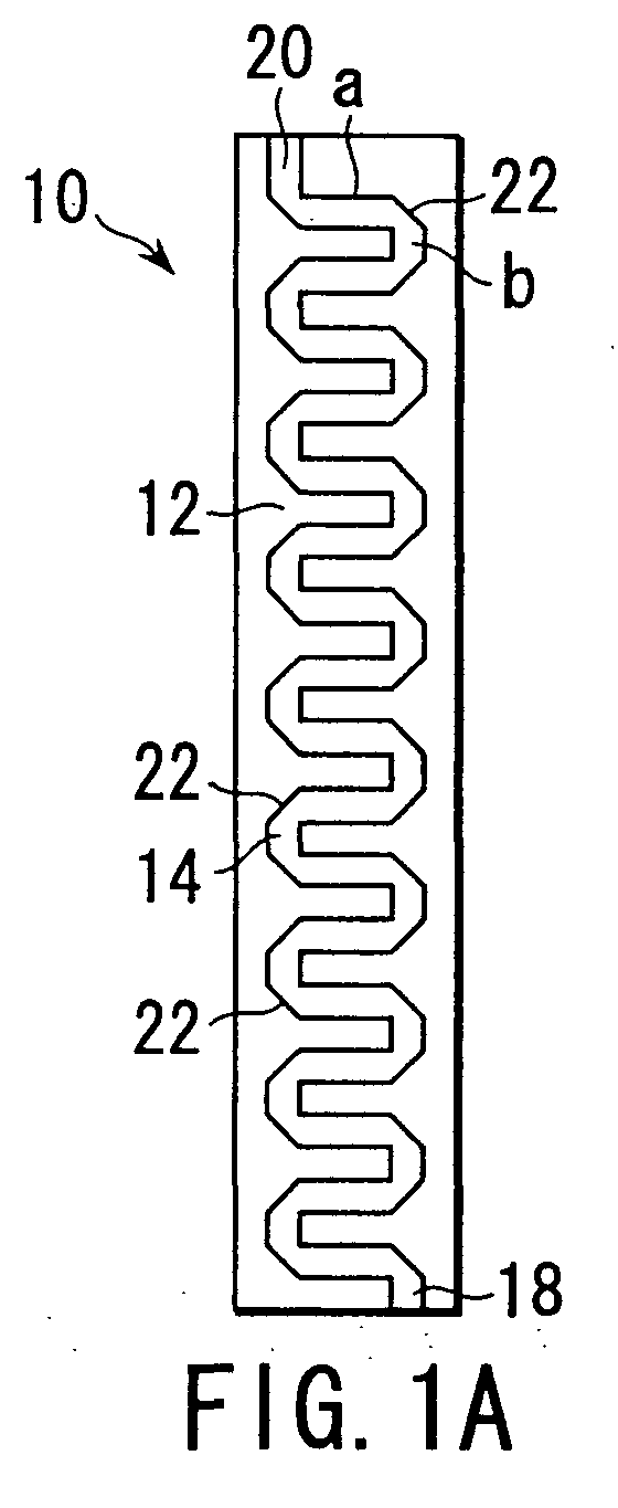
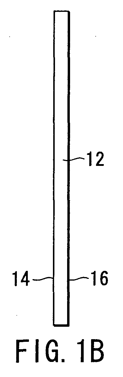
- FIGS. 1A to 1C are diagrams showing a line-shaped antenna according to a first embodiment of the present invention.
- a line-shaped antenna 10 includes an antenna element 14 having a strip-shaped conductor formed in a meander form on one surface of a dielectric substrate 12, and a metal plate 16 formed on the other surface thereof.
- the antenna element 14 has a length of substantially 1/4 wavelength, one end thereof is a power supply portion 18, and the other end is a release end 20. That is, the metal plate 16 functions as a parasitic element, not as a ground plate.
- the antenna element 14 has a width direction straight portion a extending straight in a width direction of a meander and a pitch direction straight portion b extending straight of a pitch direction of the meander, and the width direction straight portion a and pitch direction straight portion b form right angles. That is, the antenna element 14 is formed so as to be bent at right angles.
- the line-shaped antenna 10 according to the first embodiment is manufactured, for example, as follows.
- a double-sided copper foil substrate (thickness of a copper foil is 36 ⁇ m) cut in a predetermined with and length is prepared.
- the copper foil on one surface of the substrate is etched, punching-molded, or printed to form the antenna element 14.
- the line-shaped antenna 10 according to the first embodiment is characterized in that an outer edge of a portion of the strip-shaped conductor of the antenna element 14 bent at right angles is cut in an isosceles triangular shape. That is, the first embodiment is characterized in that each of chamfered portions 22 is cut along a line crossing at right angles to a line by which an angle formed by the straight portions a and b is equally divided into two. Concretely, the chamfered portion 22 is cut at an angle of 45° with respect to the pitch direction.
- the line-shaped antenna 10 having the chamfered portions 22 as shown in FIGS. 1A to 1C are experimentally manufactured.
- the dielectric substrate 12 has a length of 36 mm, width of 8 mm, and thickness of 1.6 mm.
- the antenna element 14 has a conductor width of 1 mm, conductor interval of 1 mm, and meander width of 6 mm.
- the metal plate 16 has the same length and width as those of the dielectric substrate 12.
- the line-shaped antenna 10 shown in FIGS. 2A to 2C is experimentally manufactured, and is the same as the line-shaped antenna 10 of FIGS. 1A to 1C except that the bent portions of the antenna element 14 are not chamfered.
- Changes of voltage standing wave ratios (VSWR) of a time at which the frequencies of the line-shaped antenna according to the first embodiment and conventional line-shaped antenna are changed are measured. Measurement results are shown in a graph of FIG. 3.
- a bold line with cuts (with the chamfered portions) shows properties of the line-shaped antenna according to the first embodiment, and a thin line without any cut shows the properties of the conventional line-shaped antenna.
- FIG. 4B three types of line-shaped antennas having conductor widths of 5 mm, 10 mm, and 15 mm are prepared. Moreover, the bandwidths are measured, when the size (length L of one of two equal sides of the portion chamfered in a right-angled isosceles triangle) of the chamfered portion is changed in a range of 0 to twice the conductor width W. Measurement results are shown in FIG. 4A. As shown in FIG. 4A, when the bandwidth without any chamfered portion is set to 1, and when the chamfered portions are provided, it is seen that the respective bandwidths change as follows.
- the change amount of the bandwidth is ⁇ M/2 or more, when the size of the chamfered portion is 0.7 times or more as much as the conductor width W, and the effect of the broadened band is remarkable especially in this range. Therefore, the size of the chamfered portion is preferably set to 0.7 times or more as much as the conductor width W.
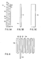
- FIGS. 5A to 5C are diagrams showing the line-shaped antenna according to a second embodiment of the present invention.
- the same part as that of FIGS. 1A to 1C is denoted with the same reference numerals, and detailed description thereof will be omitted.
- the antenna element 14 having the meandering strip-shaped conductor is formed on one surface of the dielectric substrate 12, but the metal plate is not provided on the other surface of the dielectric substrate 12.
- the band of the antenna can be broadened.
- FIG. 6 shows a third embodiment showing an example in which the line-shaped antenna according to the present invention is applied to a 2-frequencies master antenna.
- a conductor antenna is branched into two in the vicinity of a power supply portion 30 (referred to as the "branched portion"), and a first antenna element 14a is connected to a second antenna element 14b.
- the branched portion is cut substantially in a V shape, the chamfered portion 22 is formed.
- the first to third embodiments show most effective chamfered portions 22 formed by cutting the corners of the strip-shaped conductors along straight lines.
- the chamfered portion may be formed by cutting the outer surface of the (bent) corner in which the straight portions intersect each other along a curve such as a circular arc having a predetermined radius.
- the portion may of course have a shape such that the conductor is swelled to the inside of the corner, that is, such that the inner side of the corner is also chamfered.
- the antenna having a band broader than conventional can be obtained.
- a fourth embodiment is an embodiment for solving this problem.
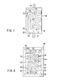
- FIG. 7 is a diagram showing the line-shaped antenna according to the fourth embodiment of the present invention.
- the line-shaped antenna according to the fourth embodiment includes the antenna element 14 having two meander patterns 14a, 14b whose meander directions are different.
- the antenna element 14 is buried in the resin molded material 12 having a flat plate shape.
- the power supply terminal 18 is formed on one end of the antenna element 14 so as to extend out of the resin molded material 12, and the fixed terminal 20 is formed on the other end of the element so as to extend out of the resin molded material 12.
- the above-described line-shaped antenna is manufactured as follows.
- a conductor pattern 40 shown in FIG. 8 is formed by punching or etching a thin metal plate (e.g., a copper plate).
- the conductor pattern 40 holds the antenna element 14 having two meander patterns 14a, 14b which are provided in a quadrangular broad frame 24 and which have different meander directions.
- the antenna element 14 is connected to the frame 24 via connection portions 26 in a plurality of positions.
- One end of the antenna element 14 is connected to the frame 24 via the power supply terminal 18.
- the other end of the antenna element 14 is connected to the frame 24 via the fixed terminal 20. Thereby, the antenna element 14 is held in a predetermined positions in the frame 24.
- FIG. 8 shows positioning holes formed in four corners of the frame 24.
- the conductor pattern 40 is set in a mold, and then the injection molding is performed.
- the conductor pattern 40 is held between an upper mold and a lower mold.
- a cavity 42 is formed in a frame shown by a two-dots chain line. Therefore, in FIG. 8, the portion outside the two-dots chain line (outer ends of the connection portions 26 of the conductor pattern 40, outer ends of the terminals 18, 20, and frame 24) is held between the molds.
- a gate for injecting a resin in the cavity 42 is provided on a surface 42a of the cavity 42 provided on the side of the fixed terminal 20 of the antenna element 14.
- the antenna element 14 of the line-shaped antenna according to the fourth embodiment has two meander patterns 14a, 14b whose meander directions are different. Therefore, the meander pattern is complicated.
- the connection portions 26 cannot be formed in some corner portions.
- the connection portions cannot be formed in corner portions T 1 , T 2 .
- These corner portions T 1 , T 2 are easily deformed by the flow of resin during the resin molding.
- the connection portion cannot be formed also in a corner portion T 4 inside the second meander pattern 14b.
- the second meander pattern 14b has a narrow meander width, and is not easily deformed, and there is no problem as it is.
- the broadened band it is preferable for the broadened band to provide the chamfered portions 22 in the outer surfaces of all the corner portions.
- the chamfered portions 22 are provided on the corner portions T 1 and T 2, which are easily deformed during the resin molding, the reduction of the mechanical strength of the portions is lowered and as a result the deformation is promoted.
- the outer surface of the portion is not chamfered, so that the mechanical strength is enhanced.
- the first and second meander patterns 14a and 14b are provided so that the pitch directions of the meanders cross at right angles to each other.
- the first meander pattern 14a has a larger meander width than that of the second meander pattern 14b.
- one end of the first meander pattern 14a in the meander width direction is provided in the vicinity of the surface 42a in which the gate of the cavity 42 is provided, and the other end thereof is provided in a position apart from the surface 42a. It is predicted that the resin flowing into the cavity during the resin molding flows substantially along the meander width direction of the first meander pattern 14a.
- the corner portion T 2 is provided in a position closer to the gate than the adjacent corner portion T 1 during the resin molding.
- the corner portion T 2 is provided in the position closer to the gate than an adjacent corner portion T 3 .
- the corner portion T 2 is closest to the gate, and the corner portions T 1 and T 3 are provided adjacent to each other to sandwich the corner portion T 2 .
- the chamfered portions outside these corner portions T 1 , T 2 , T 3 are omitted.
- the gate for injecting the resin during the resin molding usually remains as a gate trace in the resin molded material 30.
- the portions in which the connection portions of the first meander pattern 14a cannot be made, particularly the periphery of the corner portion T 2 are reinforced. Therefore, the antenna element 14 can be prevented from being deformed during the resin molding. As a result, the line-shaped antenna whose properties are stabilized can be obtained.
- three corner portions T 1 , T 2 , T 3 are not chamfered, but the other corner portions are all chamfered. Therefore, most of the corner portions are chamfered. There is little possibility that three non-chamfered corner portions T 1 , T 2 , T 3 inhibit the band enlargement.
- FIG. 10 is a diagram showing the line-shaped antenna according to a fifth embodiment of the present invention.
- FIG. 11 is a diagram showing the conductor pattern 40 for use in the line-shaped antenna according to the fifth embodiment.
- the same part as that of FIGS. 7 and 8 is denoted with the same reference numerals.
- the fillet portion 44 is provided inside the corner portions T 1 , T 3 , that is, the corner portion whose mechanical strength is weak. Thereby, the conductor width is locally thickened, and the mechanical strength is enhanced.
- the "fillet portion” is the portion 44 extending inwards from a corner portion in which straight sides intersect each other inside the antenna element 14 on the corner portion T in which the antenna element 14 is bent.
- the corner portion is reinforced. Therefore, the deformation of the corner portion does not easily occur during the resin molding.
- the conductor width of the corresponding portion is broadened. However, since the conductor width is locally broadened, the resonance frequency can be prevented from rising.
- FIGS. 12A and 12B show an example in which the corner portion is not chamfered.
- the chamfered portion 22 may be provided in the portion in which the fillet portion 44 is provided as in the first to third embodiments. In this manner, even when the chamfered portion 22 is provided, the sufficient strength of the corner portion can be kept.
- the strength is preferable for the strength to provide the fillet portion 44 also on the corner portion T 2 similarly as the corner portion T 1 .
- the fillet portions 44 are provided on the corner portions provided adjacent to each other, it is not preferable because of increasing the frequency fluctuation. This is supposedly because the electric length of a crank-shaped portion including these corner portions is remarkably reduced.
- the fillet portion 44 is provided on the corner portion T 2 closer to the resin molded material center of the antenna element 14.
- a volume of a dielectric material provided around the conductor is considered to be a cause.
- the reason is as follows. Since the conductor buried in the vicinity of the periphery of a dielectric chip (resin molded material) is positioned in the peripheral portion of the chip, a dielectric constant contributes also with an outside state (air).
- the conductor in the vicinity of the middle of the conductor chip has a small air contribution ratio as compared with the conductor provided in the peripheral portion.
- the effective dielectric constant of the conductor in the vicinity of the chip middle is high, and the wavelength reduction effect is also large. Therefore, it is considered that a slight conductor length change produces a large frequency change.
- the fillet portion is not provided on the corner portion T 2 closer to the resin molded material center of the antenna element 14, but the fillet portion 44 is provided on the corner portions T 1 , T 3 closer to the outer surface of the resin molded material 12 (on the corner portion apart from the center). This enhances the mechanical strength of whole antenna element, and further reduces the frequency fluctuation.
- the fillet portions 44 are provided both on the corner portions T 1 , T 3 .
- the outer surfaces of these corner portions T 1 , T 2 , T 3 are chamfered, but the mechanical strength of the antenna element may be more improved with no chamfers.
- the antenna element 14 may be provided integrally in the surface of the resin molded material 12.
- the cavity is formed in either one of the upper and lower molds.
- the antenna element may be set in the mold surface of the mold with no cavity formed therein in order to perform the injection molding.
- the meander pattern in the line-shaped antenna in which the antenna element including the meander pattern is formed integrally in the resin molded material, the meander pattern can be prevented from being deformed during the molding of the resin molded material. Therefore, the line-shaped antenna whose antenna properties are stabilized can be obtained.
Landscapes
- Details Of Aerials (AREA)
Abstract
Description
| Bandwidth | ||
| Antenna of the present invention with chamfered portions | Conventional antenna without chamfered portions | |
| VSWR < 3 | 259 MHz | 226 MHz |
| VSWR < 2.5 | 207 MHz | 185 MHz |
| VSWR < 2 | 154 MHz | 135 MHz |
| VSWR < 1.5 | 103 MHz | 74 MHz |
Claims (11)
- A line-shaped antenna comprising:characterized in thatan antenna element (14) in which a strip-shaped conductor is bent in a width direction of a strip,
a chamfered portion (22) is provided on an outer
edge of a bent portion of the strip-shaped conductor. - The line-shaped antenna according to claim 1, characterized in that a size of the chamfered portion (a length of one side of two equal sides of the chamfered portion in an isosceles triangular shape) is set to be 0.7 times or more as much as a conductor width of the strip-shaped conductor.
- A line-shaped antenna characterized by comprising:an antenna element (14) having a meander pattern of a strip-shaped conductor;a resin molded material (16) molded to be integral with the antenna element; anda fillet portion (44) provided on an inner surface of at least one corner portion of a plurality of corner portions of the meander pattern.
- The line-shaped antenna according to claim 3, characterized in that the corner portion on which the fillet portion is provided is a corner portion which is easily deformed during resin molding.
- The line-shaped antenna according to claim 3, characterized in that the corner portion with the fillet portion provided therein is positioned apart from a connection portion (26) which connects the meander pattern to a frame (24).
- The line-shaped antenna according to claim 3, characterized in that the antenna element (14) includes a plurality of meander patterns (14a, 14b) whose meander directions are different, and the fillet portion (44) is provided on the corner portion (T1) in which the meander direction changes.
- The line-shaped antenna according to claim 3, characterized in that the antenna element includes a first corner portion (T4) whose outer surface is chamfered, and a second corner portion (T1) whose outer surface is not chamfered and on which the fillet portion (44) is provided.
- The line-shaped antenna according to claim 7, characterized in that
when the deformation easily occurred during the resin molding, the corner portion (T2) provided on a portion close to a resin molded material center of the antenna element (14) among two adjacent corner constituting one straight line portion which is easily deformed is not chamfered, and the fillet portion (44) is provided on the corner portion (T1) provided in a portion apart from the center. - The line-shaped antenna according to claim 3, characterized in that
the antenna element includes a first meander pattern (14a) and a second meander pattern (14b) whose meander directions are different and which meander pitch directions cross at right angles to each other, and
the first meander pattern includes a first corner portion provided in a position close to a gate via which a resin is injected during resin molding and a second corner portion provided in a position apart from the first corner portion, and the fillet portion (44) is provided on a corner portion provided in a position adjacent to the corner portion provided in the position close to the gate. - The line-shaped antenna according to claim 1 or 3, characterized in that the antenna element includes a meander pattern in which two meander patterns having different meander directions and different widths are connected to each other via a connection portion, and
the connection portion and two corner portions on a broader meander pattern side connected via the connection portion are not chamfered. - The line-shaped antenna according to claim 7, characterized in that the antenna element further includes at least one of a third corner portion (T2) on which the chamfer is not formed, and a fourth corner portion (T4) having a fillet portion (44).
Applications Claiming Priority (4)
| Application Number | Priority Date | Filing Date | Title |
|---|---|---|---|
| JP2001146662 | 2001-05-16 | ||
| JP2001146662 | 2001-05-16 | ||
| JP2001378639 | 2001-12-12 | ||
| JP2001378639 | 2001-12-12 |
Publications (2)
| Publication Number | Publication Date |
|---|---|
| EP1258945A2 true EP1258945A2 (en) | 2002-11-20 |
| EP1258945A3 EP1258945A3 (en) | 2003-11-05 |
Family
ID=26615197
Family Applications (1)
| Application Number | Title | Priority Date | Filing Date |
|---|---|---|---|
| EP02010173A Withdrawn EP1258945A3 (en) | 2001-05-16 | 2002-05-14 | Line-shaped antenna |
Country Status (4)
| Country | Link |
|---|---|
| US (1) | US6894646B2 (en) |
| EP (1) | EP1258945A3 (en) |
| KR (1) | KR20020087878A (en) |
| CN (1) | CN1385924A (en) |
Cited By (1)
| Publication number | Priority date | Publication date | Assignee | Title |
|---|---|---|---|---|
| CN101055940B (en) * | 2006-04-10 | 2013-03-13 | 日立金属株式会社 | Antenna device and multiple frequency band type radio communication device using the same |
Families Citing this family (46)
| Publication number | Priority date | Publication date | Assignee | Title |
|---|---|---|---|---|
| WO2004042866A1 (en) * | 2002-11-08 | 2004-05-21 | Eung-Soon Chang | Folded monopole antenna for cellular phone |
| US6870506B2 (en) * | 2003-06-04 | 2005-03-22 | Auden Techno Corp. | Multi-frequency antenna with single layer and feeding point |
| USD587691S1 (en) * | 2004-03-29 | 2009-03-03 | Impinj, Inc. | Radio frequency identification tag antenna assembly |
| FR2869467A1 (en) * | 2004-04-23 | 2005-10-28 | Amphenol Socapex Soc Par Actio | RF COMPACT ANTENNA |
| US7202821B2 (en) * | 2004-06-18 | 2007-04-10 | Matsushita Electric Industrial Co., Ltd. | Antenna |
| WO2006098587A1 (en) * | 2005-03-15 | 2006-09-21 | Electronics And Telecommunications Research Institute | Freuqency selective surface for the filtering of freuqency band and design method thereof |
| KR100682996B1 (en) * | 2005-05-17 | 2007-02-15 | 한국전자통신연구원 | FSS Architecture for Single Frequency Band Filtering |
| EP1764866A1 (en) * | 2005-09-15 | 2007-03-21 | Infineon Tehnologies AG | Miniaturized integrated monopole antenna |
| USD592192S1 (en) * | 2005-09-30 | 2009-05-12 | Impinj, Inc. | Race flag feature for a radio frequency identification tag antenna layout |
| DE102005049820A1 (en) * | 2005-10-18 | 2007-04-19 | Benq Mobile Gmbh & Co. Ohg | Multi-resonant antenna unit, associated printed circuit board and radio communication device |
| TWI293819B (en) * | 2005-11-14 | 2008-02-21 | Chant Sincere Co Ltd | Chip antenna |
| US20070164909A1 (en) * | 2006-01-13 | 2007-07-19 | Ogawa Harry K | Embedded antenna of a mobile device |
| TW200803038A (en) * | 2006-06-23 | 2008-01-01 | Wistron Neweb Corp | A flat mini type digital television antenna |
| USD589500S1 (en) * | 2006-11-02 | 2009-03-31 | First Impression Systems, Llc | EAS antenna |
| USD555154S1 (en) * | 2007-05-11 | 2007-11-13 | Cheng Uei Precision Industry Co., Ltd. | Multi-band antenna |
| USD573589S1 (en) * | 2007-06-22 | 2008-07-22 | Skycross, Inc. | Antenna structure |
| USD573590S1 (en) * | 2007-07-24 | 2008-07-22 | Skycross, Inc. | Antenna structure |
| USD581400S1 (en) * | 2007-08-17 | 2008-11-25 | Skycross, Inc. | Antenna structure |
| JP5114177B2 (en) * | 2007-12-12 | 2013-01-09 | 富士通テン株式会社 | Information recording device |
| USD585054S1 (en) * | 2008-08-06 | 2009-01-20 | Cheng Uei Precision Industry Co., Ltd. | Multi-band antenna |
| USD608770S1 (en) * | 2008-08-21 | 2010-01-26 | Panasonic Corporation | Antenna |
| USD611039S1 (en) * | 2008-08-21 | 2010-03-02 | Panasonic Corporation | Antenna |
| USD611038S1 (en) * | 2008-08-21 | 2010-03-02 | Panasonic Corporation | Antenna |
| USD611037S1 (en) * | 2008-10-15 | 2010-03-02 | Impinj, Inc. | RFID tag antenna |
| USD602480S1 (en) * | 2008-11-14 | 2009-10-20 | Murata Manufacturing Co., Ltd. | Antenna for wireless tag |
| USD602479S1 (en) * | 2008-11-14 | 2009-10-20 | Murata Manufacturing Co., Ltd. | Antenna for wireless tag |
| US8395233B2 (en) * | 2009-06-24 | 2013-03-12 | Harris Corporation | Inductor structures for integrated circuit devices |
| USD612838S1 (en) * | 2009-09-08 | 2010-03-30 | Tracker Inc. | Antenna structure for radio tracking receiver |
| US8179221B2 (en) * | 2010-05-20 | 2012-05-15 | Harris Corporation | High Q vertical ribbon inductor on semiconducting substrate |
| TWI506864B (en) * | 2010-06-30 | 2015-11-01 | Chi Mei Comm Systems Inc | Global position system antenna |
| US8304855B2 (en) | 2010-08-04 | 2012-11-06 | Harris Corporation | Vertical capacitors formed on semiconducting substrates |
| CN102064385A (en) * | 2010-12-16 | 2011-05-18 | 上海华申泰格软件有限公司 | Fusion-packaged ultra-high frequency antenna |
| USD749063S1 (en) | 2011-02-16 | 2016-02-09 | Callas Enterprises Llc | Combined mat and eas antenna |
| USD715274S1 (en) | 2011-02-16 | 2014-10-14 | Callas Enterprises, LLC | Combined mat and EAS antenna |
| USD695278S1 (en) * | 2011-10-05 | 2013-12-10 | Upm Rfid Oy | RFID sticker |
| USD681611S1 (en) * | 2011-11-17 | 2013-05-07 | Cheng Uei Precision Industry Co., Ltd. | Antenna |
| USD749062S1 (en) | 2013-01-02 | 2016-02-09 | Callas Enterprises Llc | Combined floor mat and EAS antenna |
| USD716773S1 (en) * | 2013-09-10 | 2014-11-04 | Avery Dennison Corporation | RFID inlay |
| USD760205S1 (en) * | 2014-03-28 | 2016-06-28 | Lorom Industrial Co., Ltd. | Antenna for glass |
| USD715782S1 (en) * | 2014-04-04 | 2014-10-21 | Avery Dennison Corporation | RFID inlay |
| USD768118S1 (en) * | 2015-04-29 | 2016-10-04 | Airgain Incorporated | Antenna |
| USD773444S1 (en) * | 2016-02-25 | 2016-12-06 | Airgain Incorporated | Antenna |
| CN109560375B (en) * | 2018-11-23 | 2020-09-25 | 中山大学 | Periodic orthogonal meander line leaky-wave antenna |
| JP1654576S (en) * | 2019-06-18 | 2020-03-09 | ||
| JP1654577S (en) * | 2019-06-18 | 2020-03-09 | ||
| TWI738343B (en) * | 2020-05-18 | 2021-09-01 | 為昇科科技股份有限公司 | Meander antenna structure |
Family Cites Families (18)
| Publication number | Priority date | Publication date | Assignee | Title |
|---|---|---|---|---|
| JPS5799804A (en) | 1980-12-12 | 1982-06-21 | Toshio Makimoto | Microstrip line antenna |
| DE4005613A1 (en) | 1990-02-22 | 1991-08-29 | Vaw Ver Aluminium Werke Ag | METHOD FOR THE PRODUCTION OF GALLOSILICATES AND THEIR USE FOR THE PRODUCTION OF CATALYSTS AND / OR ADSORBENTS |
| DE4121333A1 (en) * | 1991-06-25 | 1993-01-14 | Hagenuk Telecom Gmbh | FILM ANTENNA |
| US6111545A (en) * | 1992-01-23 | 2000-08-29 | Nokia Mobile Phones, Ltd. | Antenna |
| JP2000223928A (en) * | 1999-01-28 | 2000-08-11 | Smk Corp | Antenna device |
| US5955997A (en) * | 1996-05-03 | 1999-09-21 | Garmin Corporation | Microstrip-fed cylindrical slot antenna |
| JPH1056313A (en) | 1996-08-08 | 1998-02-24 | Kokusai Electric Co Ltd | Small antenna |
| JP3669117B2 (en) * | 1997-07-23 | 2005-07-06 | 松下電器産業株式会社 | Helical antenna and manufacturing method thereof |
| US6163300A (en) * | 1997-08-07 | 2000-12-19 | Tokin Corporation | Multi-band antenna suitable for use in a mobile radio device |
| US5949383A (en) * | 1997-10-20 | 1999-09-07 | Ericsson Inc. | Compact antenna structures including baluns |
| JPH11163620A (en) | 1997-11-27 | 1999-06-18 | Sharp Corp | Frequency switching type antenna |
| US6184833B1 (en) * | 1998-02-23 | 2001-02-06 | Qualcomm, Inc. | Dual strip antenna |
| EP0954054A1 (en) * | 1998-04-30 | 1999-11-03 | Kabushiki Kaisha Yokowo | Folded antenna |
| JP3982098B2 (en) | 1999-03-15 | 2007-09-26 | ソニー株式会社 | Antenna and portable terminal device |
| US6356244B1 (en) * | 1999-03-30 | 2002-03-12 | Ngk Insulators, Ltd. | Antenna device |
| JP3788115B2 (en) * | 1999-07-23 | 2006-06-21 | 松下電器産業株式会社 | Method for manufacturing antenna device |
| JP2001111322A (en) * | 1999-10-14 | 2001-04-20 | Matsushita Graphic Communication Systems Inc | Antenna fixing structure and antenna fixing method |
| US6337663B1 (en) * | 2001-01-02 | 2002-01-08 | Auden Techno Corp. | Built-in dual frequency antenna |
-
2002
- 2002-05-14 EP EP02010173A patent/EP1258945A3/en not_active Withdrawn
- 2002-05-15 KR KR1020020026612A patent/KR20020087878A/en not_active Withdrawn
- 2002-05-15 US US10/150,138 patent/US6894646B2/en not_active Expired - Fee Related
- 2002-05-16 CN CN02119769A patent/CN1385924A/en active Pending
Cited By (1)
| Publication number | Priority date | Publication date | Assignee | Title |
|---|---|---|---|---|
| CN101055940B (en) * | 2006-04-10 | 2013-03-13 | 日立金属株式会社 | Antenna device and multiple frequency band type radio communication device using the same |
Also Published As
| Publication number | Publication date |
|---|---|
| US6894646B2 (en) | 2005-05-17 |
| EP1258945A3 (en) | 2003-11-05 |
| US20030006940A1 (en) | 2003-01-09 |
| KR20020087878A (en) | 2002-11-23 |
| CN1385924A (en) | 2002-12-18 |
Similar Documents
| Publication | Publication Date | Title |
|---|---|---|
| US6894646B2 (en) | Line-shaped antenna | |
| US7274334B2 (en) | Stacked multi-resonator antenna | |
| US7277055B2 (en) | Compact antenna | |
| KR101571345B1 (en) | 2 system for interconnecting two substrates each comprising at least one transmission line | |
| EP1605397B1 (en) | Radio frequency IC tag and method for manufacturing the same | |
| EP1270168B1 (en) | Chip antenna and method of manufacturing the same | |
| US20050057401A1 (en) | Small-size, low-height antenna device capable of easily ensuring predetermined bandwidth | |
| US9570803B2 (en) | Multi-band antenna | |
| US7642981B2 (en) | Wide-band slot antenna apparatus with constant beam width | |
| EP1223639A1 (en) | Chip antenna and method of manufacturing the same | |
| US11476580B2 (en) | Antenna and communication device | |
| EP1936739B1 (en) | Improvement to radiating slot planar antennas | |
| US20090179800A1 (en) | Antenna structure | |
| EP4075601B1 (en) | Antenna structure and wireless communication device | |
| EP1443596A1 (en) | Multi-segmented planar antenna with built-in ground plane | |
| EP1483803B1 (en) | Microwave antenna | |
| KR101891562B1 (en) | Array antenna using dual band loop antenna | |
| KR100361938B1 (en) | Resonating apparatus for a dielectric substrate | |
| CN108808253B (en) | A Cavity-Backed Slot Antenna Based on Substrate Integrated Waveguide Loaded with Shorting Pins | |
| JP2005203971A (en) | Antenna device and antenna system | |
| JP4751674B2 (en) | Planar antenna | |
| CN118315797A (en) | Patch antenna and terminal equipment | |
| KR100858969B1 (en) | Bowtie-type wideband monopole antenna with improved bandstop characteristics | |
| KR20240046428A (en) | Transmitting devices and antennas | |
| JP6232235B2 (en) | converter |
Legal Events
| Date | Code | Title | Description |
|---|---|---|---|
| PUAI | Public reference made under article 153(3) epc to a published international application that has entered the european phase |
Free format text: ORIGINAL CODE: 0009012 |
|
| AK | Designated contracting states |
Kind code of ref document: A2 Designated state(s): AT BE CH CY DE DK ES FI FR GB GR IE IT LI LU MC NL PT SE TR |
|
| AX | Request for extension of the european patent |
Free format text: AL;LT;LV;MK;RO;SI |
|
| PUAL | Search report despatched |
Free format text: ORIGINAL CODE: 0009013 |
|
| AK | Designated contracting states |
Kind code of ref document: A3 Designated state(s): AT BE CH CY DE DK ES FI FR GB GR IE IT LI LU MC NL PT SE TR |
|
| AX | Request for extension of the european patent |
Extension state: AL LT LV MK RO SI |
|
| RIC1 | Information provided on ipc code assigned before grant |
Ipc: 7H 01Q 1/24 B Ipc: 7H 01Q 1/36 B Ipc: 7H 01Q 5/00 B Ipc: 7H 01Q 1/38 A |
|
| 17P | Request for examination filed |
Effective date: 20040123 |
|
| AKX | Designation fees paid |
Designated state(s): DE |
|
| 17Q | First examination report despatched |
Effective date: 20040621 |
|
| GRAP | Despatch of communication of intention to grant a patent |
Free format text: ORIGINAL CODE: EPIDOSNIGR1 |
|
| STAA | Information on the status of an ep patent application or granted ep patent |
Free format text: STATUS: THE APPLICATION IS DEEMED TO BE WITHDRAWN |
|
| 18D | Application deemed to be withdrawn |
Effective date: 20060830 |