EP1258859A1 - Method for a segmented inverse gamma correction for a plasma display panel - Google Patents
Method for a segmented inverse gamma correction for a plasma display panel Download PDFInfo
- Publication number
- EP1258859A1 EP1258859A1 EP01112260A EP01112260A EP1258859A1 EP 1258859 A1 EP1258859 A1 EP 1258859A1 EP 01112260 A EP01112260 A EP 01112260A EP 01112260 A EP01112260 A EP 01112260A EP 1258859 A1 EP1258859 A1 EP 1258859A1
- Authority
- EP
- European Patent Office
- Prior art keywords
- gray level
- video signal
- range
- pdp
- gamma
- Prior art date
- Legal status (The legal status is an assumption and is not a legal conclusion. Google has not performed a legal analysis and makes no representation as to the accuracy of the status listed.)
- Granted
Links
- 238000000034 method Methods 0.000 title claims abstract description 70
- 238000009877 rendering Methods 0.000 abstract description 2
- 238000006243 chemical reaction Methods 0.000 description 7
- 230000000694 effects Effects 0.000 description 1
- 238000012986 modification Methods 0.000 description 1
- 230000004048 modification Effects 0.000 description 1
Images



Classifications
-
- G—PHYSICS
- G09—EDUCATION; CRYPTOGRAPHY; DISPLAY; ADVERTISING; SEALS
- G09G—ARRANGEMENTS OR CIRCUITS FOR CONTROL OF INDICATING DEVICES USING STATIC MEANS TO PRESENT VARIABLE INFORMATION
- G09G3/00—Control arrangements or circuits, of interest only in connection with visual indicators other than cathode-ray tubes
- G09G3/20—Control arrangements or circuits, of interest only in connection with visual indicators other than cathode-ray tubes for presentation of an assembly of a number of characters, e.g. a page, by composing the assembly by combination of individual elements arranged in a matrix no fixed position being assigned to or needed to be assigned to the individual characters or partial characters
- G09G3/2007—Display of intermediate tones
-
- G—PHYSICS
- G09—EDUCATION; CRYPTOGRAPHY; DISPLAY; ADVERTISING; SEALS
- G09G—ARRANGEMENTS OR CIRCUITS FOR CONTROL OF INDICATING DEVICES USING STATIC MEANS TO PRESENT VARIABLE INFORMATION
- G09G2320/00—Control of display operating conditions
- G09G2320/02—Improving the quality of display appearance
- G09G2320/0271—Adjustment of the gradation levels within the range of the gradation scale, e.g. by redistribution or clipping
-
- G—PHYSICS
- G09—EDUCATION; CRYPTOGRAPHY; DISPLAY; ADVERTISING; SEALS
- G09G—ARRANGEMENTS OR CIRCUITS FOR CONTROL OF INDICATING DEVICES USING STATIC MEANS TO PRESENT VARIABLE INFORMATION
- G09G2320/00—Control of display operating conditions
- G09G2320/02—Improving the quality of display appearance
- G09G2320/0271—Adjustment of the gradation levels within the range of the gradation scale, e.g. by redistribution or clipping
- G09G2320/0276—Adjustment of the gradation levels within the range of the gradation scale, e.g. by redistribution or clipping for the purpose of adaptation to the characteristics of a display device, i.e. gamma correction
-
- G—PHYSICS
- G09—EDUCATION; CRYPTOGRAPHY; DISPLAY; ADVERTISING; SEALS
- G09G—ARRANGEMENTS OR CIRCUITS FOR CONTROL OF INDICATING DEVICES USING STATIC MEANS TO PRESENT VARIABLE INFORMATION
- G09G3/00—Control arrangements or circuits, of interest only in connection with visual indicators other than cathode-ray tubes
- G09G3/20—Control arrangements or circuits, of interest only in connection with visual indicators other than cathode-ray tubes for presentation of an assembly of a number of characters, e.g. a page, by composing the assembly by combination of individual elements arranged in a matrix no fixed position being assigned to or needed to be assigned to the individual characters or partial characters
- G09G3/22—Control arrangements or circuits, of interest only in connection with visual indicators other than cathode-ray tubes for presentation of an assembly of a number of characters, e.g. a page, by composing the assembly by combination of individual elements arranged in a matrix no fixed position being assigned to or needed to be assigned to the individual characters or partial characters using controlled light sources
- G09G3/28—Control arrangements or circuits, of interest only in connection with visual indicators other than cathode-ray tubes for presentation of an assembly of a number of characters, e.g. a page, by composing the assembly by combination of individual elements arranged in a matrix no fixed position being assigned to or needed to be assigned to the individual characters or partial characters using controlled light sources using luminous gas-discharge panels, e.g. plasma panels
Definitions
- the present invention relates to PDPs (plasma display panels) and more particularly to a method of effecting various anti compensation processes on segmented gray level of input image on PDP, thereby significantly improving image quality of PDP.
- the relationship of input gray level (voltage) versus output brightness of color TV may be plotted as a curve (FIG. 1b).
- a Gamma ( ⁇ ) compensation process (called compensation process hereinafter) is performed on the original video signal by utilizing above physical characteristic thereof. That is, a compensation process is performed with respect to ⁇ in equation (1).
- the relationship of input brightness versus output gray level (voltage) of color TV may be plotted as a curve (FIG. 1a).
- ⁇ 0.45 (i.e., obtained from 1/2.2)
- the video signal received by color TV is converted into image for showing on screen of CRT of color TV.
- the relationship of input brightness versus output brightness of color TV may be plotted as a straight line (FIG. 1c).
- a high quality image is shown on the typical color TV without distortion.
- brightness of respective discharge unit on panel thereof is controlled by discharge number.
- brightness may be expressed in following equation (2) in terms of discharge number as below (i.e., a straight line):
- the higher discharge number the brighter of PDP. This is similar to the effect that the larger input voltage the brighter of a typical color TV.
- the relationship of input brightness versus output gray level (voltage) of PDP may be plotted as a curve (FIG. 2a).
- the relationship of input gray level (voltage) versus output brightness of PDP may be plotted as a straight line (FIG. 2b).
- video signal received by PDP is converted into image for showing on screen of PDP.
- a distorted image with poor contrast is shown on PDP.
- an anti compensation process is performed for solving above drawbacks.
- the relationship of input gray level (voltage) versus output gray level may be plotted as a curve (FIG. 3b).
- the relationship of input brightness versus output gray level (voltage) may be plotted as a curve (FIG. 3a).
- the relationship of input gray level (voltage) versus output brightness of PDP may be plotted as a straight line (FIG. 3c).
- FIGS. 3a, 3b and 3c By combining FIGS. 3a, 3b and 3c, in PDP the relationship of input brightness versus output brightness may be plotted as a straight line (FIG. 3d). In other words, a linear relationship exists between image shown on PDP and received video signal. As a result, a high quality image is shown on PDP without distortion.
- gray level of PDP is expressed as a power of 2. For example, in PDP eight bits are needed for representing 256 gray levels.
- an image is shown on PDP.
- the previous improvement technique has a disadvantage. That is, a non-integer number (e.g., decimal) can not be expressed by a digital signal. Hence, the decimal has to be converted into an integer.
- a smaller ⁇ is used in the anti compensation process with respect to the video signal in a range of low gray level for increasing the gray level in the range of low gray level.
- a larger ⁇ is used in the anti compensation process with respect to the video signal in a range of high gray level for increasing a gradient in the range of high gray level , thereby obtaining a sharp contrast of image,, improving image quality, and rendering an enhanced image brightness.
- FIGS. 4 to 6 where a method according to the invention is illustrated by respective graphs.
- a processing is performed on the video signal for dividing it into at least two segments based on gray level thereof.
- various anti compensation processes are performed on the video signal in respective segment so as to increase the number of gray level of video signal in the range of low gray level and increase gray level (or brightness) gradient of video signal in the range of high gray level.
- image quality of PDP is greatly improved.
- a false contour is not easily occurred in the range of low gray level. Consequently, a sharp contrast is occurred in the range of high gray level.
- a difference between two gray levels in the range of high gray level is distinguishable visually, resulting in an enhanced image brightness.
- the gray level of an image shown on a typical color TV may be varied depending on input voltage by utilizing the physical characteristic of CRT of color TV. Further, gray level of an output image is related to that of an input video signal.
- an anti compensation process is performed on the received video signal for obtaining an improved image brightness on PDP.
- brightness of an input image of PDP may be expressed in terms of an output gray level.
- a plurality of ⁇ having values smaller than 2.2 e.g., 2.0, 1.8, and 1.6
- ⁇ the higher the output gray level in the range of low gray level.
- a maximum brightness of a PDP is 500 cd/m 2 if gray level thereof is 256.
- a control circuit of PDP will be enabled to divide video signal into three segments based on gray level thereof.
- a plurality of anti compensation processes are performed on the video signal in respective segment with respect to various ⁇ s.
- the number of gray level in the range of low gray level is increased and gradient in the range of high gray level is also increased. As a result, a false contour is not easily occurred in the range of low gray level. Further, a sharp contrast of output image is obtained in the range of high gray level, thereby greatly improving the image quality of PDP.
Landscapes
- Engineering & Computer Science (AREA)
- Physics & Mathematics (AREA)
- Computer Hardware Design (AREA)
- General Physics & Mathematics (AREA)
- Theoretical Computer Science (AREA)
- Control Of Gas Discharge Display Tubes (AREA)
- Control Of Indicators Other Than Cathode Ray Tubes (AREA)
- Picture Signal Circuits (AREA)
Abstract
Description
- The present invention relates to PDPs (plasma display panels) and more particularly to a method of effecting various anti compensation processes on segmented gray level of input image on PDP, thereby significantly improving image quality of PDP.
- The brightness of a typical color television (TV) may be expressed in following equation (1) in terms of input voltage by utilizing the physical characteristic of cathode ray tube (CRT) of color TV:
- As to recently available PDPs (plasma display panels) brightness of respective discharge unit on panel thereof is controlled by discharge number. Hence, brightness may be expressed in following equation (2) in terms of discharge number as below (i.e., a straight line):
- Referring to FIGS. 2a, 2b and 2c, a compensation process is performed on received video signal by PDP by substituting γ = 0.45 into equation (1) by similarly utilizing the physical characteristic of typical color TV. As such, the relationship of input brightness versus output gray level (voltage) of PDP may be plotted as a curve (FIG. 2a). Further, the relationship of input gray level (voltage) versus output brightness of PDP may be plotted as a straight line (FIG. 2b). Furthermore, video signal received by PDP is converted into image for showing on screen of PDP. Hence, the relationship of input brightness versus output brightness of PDP may be plotted as a curve (FIG. 2c) by similarly substituting γ = 0.45 into equation (1). As a result, a distorted image with poor contrast is shown on PDP.
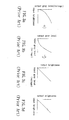
- Typically, an anti compensation process is performed for solving above drawbacks. In detail, in one example, an anti compensation process is performed on received video signal by PDP by substituting γ = 2.2 into equation (1). As such, in PDP the relationship of input gray level (voltage) versus output gray level may be plotted as a curve (FIG. 3b). In another example, an anti compensation process is performed on received video signal by PDP by substituting γ = 0.45 into equation (1). Hence, in PDP the relationship of input brightness versus output gray level (voltage) may be plotted as a curve (FIG. 3a). As to image shown on PDP, the relationship of input gray level (voltage) versus output brightness of PDP may be plotted as a straight line (FIG. 3c). By combining FIGS. 3a, 3b and 3c, in PDP the relationship of input brightness versus output brightness may be plotted as a straight line (FIG. 3d). In other words, a linear relationship exists between image shown on PDP and received video signal. As a result, a high quality image is shown on PDP without distortion.
- As to current PDPs, signal input/output and processing are done by a digital technique. Moreover, in most cases gray level of PDP is expressed as a power of 2. For example, in PDP eight bits are needed for representing 256 gray levels. Typically, in performing a compensation process an analog-to-digital conversion is performed on video signal prior to substituting γ = 0.45 into equation (1). Then an anti compensation process is performed by substituting γ = 2.2 into equation (1) for effecting an inverse transform on video signal. Finally, an image is shown on PDP. However, the previous improvement technique has a disadvantage. That is, a non-integer number (e.g., decimal) can not be expressed by a digital signal. Hence, the decimal has to be converted into an integer. In the case of the original video signal having 256 gray levels, the number of gray level is reduced to 184 after first being processed in a analog-to-digital conversion and subsequently by substituting γ = 2.2 into equation (1) for performing an anti compensation process thereafter. In another case that the original video signal having a gray level in the range of 0 to 40, the number of gray level is reduced to 5 (e.g.,
gray level gray level of original video signal gray level after γ = 2.2 conversion gray level after γ = 2.0 conversion gray level after γ = 1.8 conversion gray level after γ = 1.6 conversion 0-20 0 0-1 0-2 0-4 21-28 1 1-3 2-4 4-7 29-33 2 3-4 5-6 7-9 34-38 3 4-5 6-8 10-12 39-42 4 5-6 8-9 12-14 43-46 5 7-8 10-11 14-16 ... ... ... ... ... 47-61 6-10 8-14 12-19 14-25 Total gray level = 62 Total gray level = 11 Total gray level = 15 Total gray level = 20 Total gray level = 26 - Hence, a problem of insufficient gray level of video signal is occurred in the range of low gray level after such anti compensation process. And in turn a false contour is occurred in the range of low gray level. Consequently, a poor contrast is occurred in the range of high gray level due to extremely low gray level (or brightness) gradient. As a result, a difference between two gray levels is undistinguishable visually.
- It is thus an object of the present invention to provide a process of effecting various anti compensation processes on input image on a plasma display panel comprising the steps of a) performing a Gamma (i.e., γ = 0.45) compensation process on a video signal received by the PDP with respect to a γ ; b) dividing the video signal into at least two segments based on a gray level thereof; and c) performing a variety of anti compensation processes on the video signal in respective segment. A smaller γ is used in the anti compensation process with respect to the video signal in a range of low gray level for increasing the gray level in the range of low gray level. Similarly, a larger γ is used in the anti compensation process with respect to the video signal in a range of high gray level for increasing a gradient in the range of high gray level , thereby obtaining a sharp contrast of image,, improving image quality, and rendering an enhanced image brightness.
- The above and other objects, features and advantages of the present invention will become apparent from the following detailed description taken with the accompanying drawings.
-
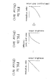
- FIG. 1a is a graph showing a relationship of input brightness versus output gray level (voltage) of a conventional color TV;
- FIG. 1b is a graph showing a relationship of input gray level (voltage) versus output brightness of the conventional color TV;
- FIG. 1c is a graph showing a relationship of input brightness versus output brightness of the conventional color TV;
- FIG. 2a is a graph showing a relationship of input brightness versus output gray level (voltage) of a conventional plasma display panel (PDP);
- FIG. 2b is a graph showing a relationship of input gray level (voltage) versus output brightness of the conventional PDP;
- FIG. 2c is a graph showing a relationship of input brightness versus output brightness of the conventional PDP;
- FIG. 3a is a graph showing a relationship of input brightness versus output gray level (voltage) of the conventional PDP after an anti compensation process is performed thereon;
- FIG. 3b is a graph showing a relationship of input gray level (voltage) versus output gray level of the conventional PDP after the anti compensation process is performed thereon;
- FIG. 3c is a graph showing a relationship of input gray level (voltage) versus output brightness of the conventional PDP after the anti compensation process is performed thereon;
- FIG. 3d is a graph showing a relationship of input brightness versus output brightness of the conventional PDP after the anti compensation process is performed thereon;
- FIG. 4 is a graph showing a relationship of input gray level versus output gray level gradient after performing a method of effecting various anti compensation processes on segmented gray level of input image on PDP according to the invention where three Gamma values are used;
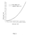
- FIG. 5 is a graph similar to FIG. 4 showing a relationship of input gray level versus output gray level where single Gamma and segmented Gamma curves are plotted for comparison; and
- FIG. 6 is a graph similar to FIG. 4 showing a relationship of input gray level versus output brightness where single Gamma and segmented Gamma curves are plotted for comparison.
-
- Referring to FIGS. 4 to 6, where a method according to the invention is illustrated by respective graphs. Before the method performs an anti compensation process on video signal received by PDP, (i.e., a compensation process is performed on the video signal with respect to γ = 0.45 in equation (1)), a processing is performed on the video signal for dividing it into at least two segments based on gray level thereof. Then various anti compensation processes are performed on the video signal in respective segment so as to increase the number of gray level of video signal in the range of low gray level and increase gray level (or brightness) gradient of video signal in the range of high gray level. As a result, image quality of PDP is greatly improved. Further, a false contour is not easily occurred in the range of low gray level. Consequently, a sharp contrast is occurred in the range of high gray level. As an end, a difference between two gray levels in the range of high gray level is distinguishable visually, resulting in an enhanced image brightness.
- The gray level of an image shown on a typical color TV may be varied depending on input voltage by utilizing the physical characteristic of CRT of color TV. Further, gray level of an output image is related to that of an input video signal. Hence, an output gray level of a typical color TV may be expressed in following equation (3) by deriving itself from equation (1):
- As stated above, a compensation process is performed on the video signal with respect to γ = 0.45 in equation (1)). Thereafter, an anti compensation process is performed on the received video signal for obtaining an improved image brightness on PDP. As a result, brightness of an input image of PDP may be expressed in terms of an output gray level. Similarly, an output gray level of PDP may be expressed in following equation (4) by deriving itself from equation (1):
gray level of original video signal gray level after γ = 2.2 conversion 0-14 0 15-24 1 25-31 2 32-36 3 37-40 4 41-44 5 45-48 6 49-51 7 52-54 8 55-57 9 58-59 10 ... ... 255 255 Total gray level =256 Total gray level = 184 - As to the higher gray level in the range of low gray level, it means that a false contour is not easily occurred. Further, gradient of PDP may be expressed in following equation (5) by differentiating equation (3):
- In view of equation (5), it is found that there is a substantially linear relationship between brightness of PDP and output gray level. Hence, the contrast of image becomes poorer as gradient of output image of PDP becomes smaller. In other words, the contrast of image becomes sharper as gradient of output image of PDP becomes larger. In following cases that a plurality of γ s having values larger than 2.2 (e.g., 2.4 and 2.6) are substituted into γ in equation (5) for obtaining respective output gray level. It is found that the larger the γ the higher the output gray level in the range of high gray level (FIG. 4). This means that the contrast of image becomes sharper. That is, a gray level difference in the range of high gray level of output image is easier to distinguish visually.
- Above fact is obtained and utilized by the invention in which before the method of the invention performs an anti compensation process on the video signal received by PDP, (i.e., a compensation process is performed on the video signal with respect to γ = 0.45 in equation (1)), a processing is performed on the video signal for dividing it into at least two segments based on gray level thereof. Then a plurality of anti compensation processes are performed on the video signal in respective segment with respect to various γ s. A smaller γ is used in the anti compensation process with respect to video signal in the range of low gray level for increasing the number of gray level therein. As a result, a false contour is not easily occurred in the range of low gray level. In contrast, a larger γ is used in the anti compensation process with respect to video signal in the range of high gray level for increasing the number of gray level therein. As a result, a sharp contrast of image is obtained, thereby greatly improving the image quality of PDP.
- In one embodiment of the invention, a maximum brightness of a PDP is 500 cd/m2 if gray level thereof is 256. Also, an anti compensation process on video signal received by PDP is already performed with respect to γ = 0.45 in equation (1). Thus when video signal is received by PDP a control circuit of PDP will be enabled to divide video signal into three segments based on gray level thereof. Then a plurality of anti compensation processes are performed on the video signal in respective segment with respect to various γ s. A γ smaller than 2.2 (e.g., γ = 1.6) is used in the anti compensation process with respect to video signal in the range of low gray level for increasing the number of gray level therein. Similarly, a γ = 2.2 is used in the anti compensation process with respect to video signal in the range of intermediate gray level. A γ larger than 2.2 (e.g., γ = 2.6) is used in the anti compensation process with respect to video signal in the range of high gray level. After the invention performing above anti compensation processes, as to output image of PDP, the number of gray level in the range of low gray level is increased and gradient in the range of high gray level is also increased. As a result, a false contour is not easily occurred in the range of low gray level. Further, a sharp contrast of output image is obtained in the range of high gray level, thereby greatly improving the image quality of PDP.
- While the invention has been described by means of specific embodiments, numerous modifications and variations could be made thereto by those skilled in the art without departing from the scope and spirit of the invention set forth in the claims.
Claims (7)
- A process of effecting various anti compensation processes on input image on a plasma display panel, said process comprising the steps of:a) performing a gamma compensation process on a video signal received by said PDP with respect to a first gamma;b) dividing said video signal into at least two segments based on a gray level thereof; andc) performing a variety of anti compensation processes on said video signal in respective segment.
- The process of claim 1, wherein in said step c) a second gamma smaller than said first gamma is used in said anti compensation process with respect to said video signal in a range of low gray level for increasing said gray level in said range of low gray level.
- The process of claim 1, wherein in said step c) a third gamma larger than said first gamma is used in said anti compensation process with respect to said video signal in a range of high gray level for increasing a gradient in said range of high gray level, thereby obtaining a sharp contrast of said image.
- The process of claim 3, wherein said gamma compensation process has been performed on said video signal received by said PDP in a following equation:
- The process of claim 4, wherein a fourth gamma smaller than 2.2 is used in said anti compensation process with respect to said video signal in said range of low gray level.
- The process of claim 4, wherein a fifth gamma equal to 2.2 is used in said anti compensation process with respect to said video signal in said range of intermediate gray level.
- The process of claim 4, wherein a sixth gamma larger than 2.2 is used in said anti compensation process with respect to said video signal in said range of high gray level.
Priority Applications (1)
| Application Number | Priority Date | Filing Date | Title |
|---|---|---|---|
| EP01112260.3A EP1258859B1 (en) | 2001-05-18 | 2001-05-18 | Method for a segmented inverse gamma correction for a plasma display panel |
Applications Claiming Priority (1)
| Application Number | Priority Date | Filing Date | Title |
|---|---|---|---|
| EP01112260.3A EP1258859B1 (en) | 2001-05-18 | 2001-05-18 | Method for a segmented inverse gamma correction for a plasma display panel |
Publications (2)
| Publication Number | Publication Date |
|---|---|
| EP1258859A1 true EP1258859A1 (en) | 2002-11-20 |
| EP1258859B1 EP1258859B1 (en) | 2015-07-08 |
Family
ID=8177481
Family Applications (1)
| Application Number | Title | Priority Date | Filing Date |
|---|---|---|---|
| EP01112260.3A Expired - Lifetime EP1258859B1 (en) | 2001-05-18 | 2001-05-18 | Method for a segmented inverse gamma correction for a plasma display panel |
Country Status (1)
| Country | Link |
|---|---|
| EP (1) | EP1258859B1 (en) |
Cited By (5)
| Publication number | Priority date | Publication date | Assignee | Title |
|---|---|---|---|---|
| WO2005014296A1 (en) | 2003-08-05 | 2005-02-17 | Hueck Folien Gmbh & Co. Kg | Printed strip-type materials, especially for covering containers |
| CN101075428B (en) * | 2007-06-26 | 2010-07-21 | 四川长虹电器股份有限公司 | Multi-segment Gamma Curve Correction Method |
| CN101546509B (en) * | 2009-04-23 | 2011-08-10 | 北京德为视讯科技股份有限公司 | Method for generating target Gamma curve of display |
| CN110890058A (en) * | 2019-12-06 | 2020-03-17 | 长春希达电子技术有限公司 | Point-by-point correction method of transformation coefficient matrix |
| CN114639346A (en) * | 2022-04-20 | 2022-06-17 | 武汉天马微电子有限公司 | Mura compensation method, apparatus, device, storage medium and computer program product |
Citations (4)
| Publication number | Priority date | Publication date | Assignee | Title |
|---|---|---|---|---|
| JPH06311394A (en) | 1993-04-21 | 1994-11-04 | Fujitsu General Ltd | Gamma correction circuit |
| JPH08317250A (en) | 1995-05-19 | 1996-11-29 | Fujitsu General Ltd | Dynamic video control circuit |
| EP0831643A2 (en) * | 1996-09-18 | 1998-03-25 | Matsushita Electric Industrial Co., Ltd. | Plasma display panel and method of controlling brightness of the same |
| EP0947975A1 (en) * | 1998-04-02 | 1999-10-06 | Hitachi, Ltd. | Gamma correction circuit |
-
2001
- 2001-05-18 EP EP01112260.3A patent/EP1258859B1/en not_active Expired - Lifetime
Patent Citations (4)
| Publication number | Priority date | Publication date | Assignee | Title |
|---|---|---|---|---|
| JPH06311394A (en) | 1993-04-21 | 1994-11-04 | Fujitsu General Ltd | Gamma correction circuit |
| JPH08317250A (en) | 1995-05-19 | 1996-11-29 | Fujitsu General Ltd | Dynamic video control circuit |
| EP0831643A2 (en) * | 1996-09-18 | 1998-03-25 | Matsushita Electric Industrial Co., Ltd. | Plasma display panel and method of controlling brightness of the same |
| EP0947975A1 (en) * | 1998-04-02 | 1999-10-06 | Hitachi, Ltd. | Gamma correction circuit |
Cited By (6)
| Publication number | Priority date | Publication date | Assignee | Title |
|---|---|---|---|---|
| WO2005014296A1 (en) | 2003-08-05 | 2005-02-17 | Hueck Folien Gmbh & Co. Kg | Printed strip-type materials, especially for covering containers |
| CN101075428B (en) * | 2007-06-26 | 2010-07-21 | 四川长虹电器股份有限公司 | Multi-segment Gamma Curve Correction Method |
| CN101546509B (en) * | 2009-04-23 | 2011-08-10 | 北京德为视讯科技股份有限公司 | Method for generating target Gamma curve of display |
| CN110890058A (en) * | 2019-12-06 | 2020-03-17 | 长春希达电子技术有限公司 | Point-by-point correction method of transformation coefficient matrix |
| CN114639346A (en) * | 2022-04-20 | 2022-06-17 | 武汉天马微电子有限公司 | Mura compensation method, apparatus, device, storage medium and computer program product |
| CN114639346B (en) * | 2022-04-20 | 2023-07-21 | 武汉天马微电子有限公司 | Mura compensation method, device, equipment, storage medium and computer program product |
Also Published As
| Publication number | Publication date |
|---|---|
| EP1258859B1 (en) | 2015-07-08 |
Similar Documents
| Publication | Publication Date | Title |
|---|---|---|
| US20020176024A1 (en) | Method of effecting various anti compensation processes on segmented gray level of input image on plasma display panel | |
| US9743073B2 (en) | Image processing device with image compensation function and image processing method thereof | |
| US6600517B1 (en) | System and method for improving the sharpness of a video image | |
| US20050237316A1 (en) | Image processing method for a TFT LCD | |
| JP2005175735A (en) | Video signal processing apparatus, television receiver using the same, and video signal processing method | |
| JPH11288241A (en) | Gamma correction circuit | |
| WO2006115784A2 (en) | Method and system for automatic color hue and color saturation adjustment of a pixel from a video source | |
| CN100397448C (en) | Image gray scale subsection inverse compensation method for input plasma plane display | |
| JP2002534007A (en) | Circuits and methods for digital correction of a linear approximation of gamma | |
| CN1148963C (en) | Image conversion apparatus and method therefor | |
| CN100382568C (en) | Method of Dynamic Contrast Improvement | |
| US6774873B2 (en) | Method for implementing error diffusion on plasma display panel | |
| EP1258859B1 (en) | Method for a segmented inverse gamma correction for a plasma display panel | |
| JPH06350943A (en) | Picture processing circuit | |
| US8289348B2 (en) | Image signal processing device | |
| KR20020089876A (en) | Method of effecting various anti compensation processes on segmented gray level of input image on plasma display panel | |
| JP4379029B2 (en) | Image processing apparatus, image processing method, and image projection apparatus | |
| JP2000197071A (en) | White balance adjustment circuit for matrix type display device and its method | |
| EP1262941A1 (en) | Method for implementing error diffusion on plasma display panel | |
| CN1171190C (en) | Brightness compensation method and device for plasma display | |
| KR100508306B1 (en) | An Error Diffusion Method based on Temporal and Spatial Dispersion of Minor Pixels on Plasma Display Panel | |
| KR100669042B1 (en) | How to Implement Error Diffusion on Plasma Display Panels | |
| JPH08317321A (en) | Image display device | |
| EP2499831B1 (en) | A method of digital signal processing | |
| CN1386005A (en) | Error diffusion method for plasma plane display |
Legal Events
| Date | Code | Title | Description |
|---|---|---|---|
| PUAI | Public reference made under article 153(3) epc to a published international application that has entered the european phase |
Free format text: ORIGINAL CODE: 0009012 |
|
| AK | Designated contracting states |
Kind code of ref document: A1 Designated state(s): AT BE CH CY DE DK ES FI FR GB GR IE IT LI LU MC NL PT SE TR |
|
| AX | Request for extension of the european patent |
Free format text: AL;LT;LV;MK;RO;SI |
|
| 17P | Request for examination filed |
Effective date: 20030319 |
|
| AKX | Designation fees paid |
Designated state(s): DE FR GB IT NL |
|
| 17Q | First examination report despatched |
Effective date: 20071115 |
|
| RAP1 | Party data changed (applicant data changed or rights of an application transferred) |
Owner name: CPT TECHNOLOGY (GROUP) CO., LTD. |
|
| GRAP | Despatch of communication of intention to grant a patent |
Free format text: ORIGINAL CODE: EPIDOSNIGR1 |
|
| INTG | Intention to grant announced |
Effective date: 20150211 |
|
| GRAS | Grant fee paid |
Free format text: ORIGINAL CODE: EPIDOSNIGR3 |
|
| GRAA | (expected) grant |
Free format text: ORIGINAL CODE: 0009210 |
|
| AK | Designated contracting states |
Kind code of ref document: B1 Designated state(s): DE FR GB IT NL |
|
| REG | Reference to a national code |
Ref country code: GB Ref legal event code: FG4D |
|
| REG | Reference to a national code |
Ref country code: DE Ref legal event code: R096 Ref document number: 60149437 Country of ref document: DE |
|
| REG | Reference to a national code |
Ref country code: NL Ref legal event code: FP |
|
| REG | Reference to a national code |
Ref country code: DE Ref legal event code: R097 Ref document number: 60149437 Country of ref document: DE |
|
| REG | Reference to a national code |
Ref country code: FR Ref legal event code: PLFP Year of fee payment: 16 |
|
| PLBE | No opposition filed within time limit |
Free format text: ORIGINAL CODE: 0009261 |
|
| STAA | Information on the status of an ep patent application or granted ep patent |
Free format text: STATUS: NO OPPOSITION FILED WITHIN TIME LIMIT |
|
| 26N | No opposition filed |
Effective date: 20160411 |
|
| REG | Reference to a national code |
Ref country code: FR Ref legal event code: PLFP Year of fee payment: 17 |
|
| REG | Reference to a national code |
Ref country code: FR Ref legal event code: PLFP Year of fee payment: 18 |
|
| PGFP | Annual fee paid to national office [announced via postgrant information from national office to epo] |
Ref country code: GB Payment date: 20180301 Year of fee payment: 18 |
|
| PGFP | Annual fee paid to national office [announced via postgrant information from national office to epo] |
Ref country code: FR Payment date: 20180212 Year of fee payment: 18 |
|
| PGFP | Annual fee paid to national office [announced via postgrant information from national office to epo] |
Ref country code: DE Payment date: 20180214 Year of fee payment: 18 |
|
| PGFP | Annual fee paid to national office [announced via postgrant information from national office to epo] |
Ref country code: NL Payment date: 20180525 Year of fee payment: 18 Ref country code: IT Payment date: 20180523 Year of fee payment: 18 |
|
| REG | Reference to a national code |
Ref country code: DE Ref legal event code: R119 Ref document number: 60149437 Country of ref document: DE |
|
| REG | Reference to a national code |
Ref country code: NL Ref legal event code: MM Effective date: 20190601 |
|
| GBPC | Gb: european patent ceased through non-payment of renewal fee |
Effective date: 20190518 |
|
| PG25 | Lapsed in a contracting state [announced via postgrant information from national office to epo] |
Ref country code: IT Free format text: LAPSE BECAUSE OF NON-PAYMENT OF DUE FEES Effective date: 20190518 Ref country code: GB Free format text: LAPSE BECAUSE OF NON-PAYMENT OF DUE FEES Effective date: 20190518 Ref country code: NL Free format text: LAPSE BECAUSE OF NON-PAYMENT OF DUE FEES Effective date: 20190601 Ref country code: DE Free format text: LAPSE BECAUSE OF NON-PAYMENT OF DUE FEES Effective date: 20191203 |
|
| PG25 | Lapsed in a contracting state [announced via postgrant information from national office to epo] |
Ref country code: FR Free format text: LAPSE BECAUSE OF NON-PAYMENT OF DUE FEES Effective date: 20190531 |