EP1257061A2 - Wireless user terminal and system having signal clipping circuit for switched capacitor sigma delta analog to digital converters - Google Patents
Wireless user terminal and system having signal clipping circuit for switched capacitor sigma delta analog to digital converters Download PDFInfo
- Publication number
- EP1257061A2 EP1257061A2 EP02100428A EP02100428A EP1257061A2 EP 1257061 A2 EP1257061 A2 EP 1257061A2 EP 02100428 A EP02100428 A EP 02100428A EP 02100428 A EP02100428 A EP 02100428A EP 1257061 A2 EP1257061 A2 EP 1257061A2
- Authority
- EP
- European Patent Office
- Prior art keywords
- signal
- coupled
- user terminal
- switch
- analog
- Prior art date
- Legal status (The legal status is an assumption and is not a legal conclusion. Google has not performed a legal analysis and makes no representation as to the accuracy of the status listed.)
- Ceased
Links
- 239000003990 capacitor Substances 0.000 title abstract description 5
- 238000004891 communication Methods 0.000 claims description 9
- 230000008878 coupling Effects 0.000 claims description 6
- 238000010168 coupling process Methods 0.000 claims description 6
- 238000005859 coupling reaction Methods 0.000 claims description 6
- 238000010586 diagram Methods 0.000 description 7
- 238000012545 processing Methods 0.000 description 4
- 239000000969 carrier Substances 0.000 description 3
- 230000001413 cellular effect Effects 0.000 description 3
- 238000006243 chemical reaction Methods 0.000 description 3
- 230000007246 mechanism Effects 0.000 description 3
- 230000003595 spectral effect Effects 0.000 description 3
- 230000009134 cell regulation Effects 0.000 description 2
- 230000005236 sound signal Effects 0.000 description 2
- 238000006467 substitution reaction Methods 0.000 description 2
- 101100458289 Drosophila melanogaster msps gene Proteins 0.000 description 1
- XUIMIQQOPSSXEZ-UHFFFAOYSA-N Silicon Chemical compound [Si] XUIMIQQOPSSXEZ-UHFFFAOYSA-N 0.000 description 1
- 238000007792 addition Methods 0.000 description 1
- 230000010267 cellular communication Effects 0.000 description 1
- 238000001914 filtration Methods 0.000 description 1
- 238000000034 method Methods 0.000 description 1
- 238000010295 mobile communication Methods 0.000 description 1
- 238000012986 modification Methods 0.000 description 1
- 230000004048 modification Effects 0.000 description 1
- 229910052710 silicon Inorganic materials 0.000 description 1
- 239000010703 silicon Substances 0.000 description 1
- 238000001228 spectrum Methods 0.000 description 1
- 238000012360 testing method Methods 0.000 description 1
Images


Classifications
-
- H—ELECTRICITY
- H03—ELECTRONIC CIRCUITRY
- H03M—CODING; DECODING; CODE CONVERSION IN GENERAL
- H03M3/00—Conversion of analogue values to or from differential modulation
- H03M3/30—Delta-sigma modulation
- H03M3/458—Analogue/digital converters using delta-sigma modulation as an intermediate step
- H03M3/478—Means for controlling the correspondence between the range of the input signal and the range of signals the converter can handle; Means for out-of-range indication
- H03M3/48—Means for controlling the correspondence between the range of the input signal and the range of signals the converter can handle; Means for out-of-range indication characterised by the type of range control, e.g. limiting
Definitions
- This invention relates generally to the field of electronic systems and, in particular, to a wireless user terminal and system having signal clipping circuits for switched capacitor sigma delta analog-to-digital converters included within audio codec systems.
- the codifier/decodifier is the algorithm that handles the coding and decoding of audio signals within an electronic system.
- an audio CODEC is a custom mixed-signal core providing analog-to-digital (A/D) and digital-to-analog (D/A) conversion.
- a simple serial interface is used to exchange digital data (D/A input and A/D output) between the application specific integrated circuit (ASIC) and CODEC core.
- Prior art CODEC features delta-sigma A/D and D/A oversampled converters and low power dissipation.
- a typical uplink channel for a mobile phone voiceband or audio CODEC includes a microphone, amplifier, sigma-delta analog-to-digital converter (ADC) and a digital filter coupled together on one chip.
- This first chip couples to a digital signal processor for processing the digital signal received.
- Another chip includes a radio frequency (RF) modulator which is coupled to a last component that includes a RF power amplifier.
- RF radio frequency
- the signal is transmitted over an antenna to a downlink channel for the mobile phone voiceband CODEC.
- the audio CODEC receives an analog voice signal through the microphone and converts it to a digital signal.
- the digital signal is forwarded to a digital signal processor for processing.
- This signal is transmitted to a receiver. In the receiver, the digital signal is processed through the digital signal processor and forwarded to a D/A converter.
- the analog signal is fed to a speaker.
- the sigma-delta ADC is scaled for a maximum output corresponding to the +3dbm0 code of the pulse code modulation (PCM) data.
- the analog signal corresponding to this digital upscale value is far less than the maximum allowable dynamic range, which usually is limited by the supply range. This fact could potentially overload the A/D and consequently the digital filter.
- An FCC test mandatory in the U.S., falls under this category.
- First and second order sigma delta analog modulators are inherently stable under large input level variations. Higher order modulators, however, can become unstable during the overload condition. Clipping the input signal to a predetermined safe operation level, prevents the modulator from going unstable, without having the need to recover stability after the overloading condition is removed. In other cases, even inherently stable sigma-delta structures have to be protected by a clipping mechanism to prevent post digital filtering from generation of a rail-to-rail digital representation of a quasi-square wave which can over-modulate the RF channel in a typical transmit CODEC channel for wireless applications.
- the signal is fed to the A/D directly from external sources, such as a microphone or an RF mixer. Accordingly, many audio CODECs no longer include the microphone and amplifier. Thus, there is a need for a wireless user terminal and system that incorporate a sigma-delta analog-to-digital converter (ADC) that is free of overshoot and settling issues.
- ADC analog-to-digital converter
- a wireless user terminal and system that implement a mixed signal CODEC including an improved sigma-delta ADC limits input signals into a switched capacitor configuration and avoids adding circuit overhead in the signal path. Additionally, the improved sigma-delta ADC substantially reduces overshoot and settling problems common in user terminals.
- This improved sigma-delta ADC having an input signal and an output signal, includes a switch, a clipping circuit, and a sigma-delta ADC. It solves the clipping signal problem in wireless user terminals by limiting the signal right at the input of the sigma-delta ADC.
- the clipping circuit couples to the switch and the sigma-delta ADC for switching the voltage applied to the sigma-delta ADC between the input signal and at least one threshold voltage.
- the fixed threshold voltage is applied to the sigma-delta ADC, which converts fixed threshold voltage into a digital signal.
- the incoming signal is applied to the sigma-delta ADC, which converts the incoming signal.
- the fixed threshold voltage is applied to the sigma-delta ADC, which converts fixed threshold voltage.
- the incoming signal is applied to the sigma-delta ADC, which converts the incoming signal.
- a circuit is presented here, that clips the incoming signal to predetermined levels without disturbing the signal path and adding little overhead to the power and area requirements.
- analog clipping circuits 40 and 42 are coupled to the differential inputs of the sigma-delta A/D 26, to avoid overdriving the sigma-delta A/D 26.
- the analog clipping circuits 40 and 42 add minimum overhead in area and power.
- the maximum allowable dynamic range at the input of the sigma delta A/D 26 is a minimum of 0.625 volts and a maximum 2.375 volts.
- the fully differential signal is 3.5 volts (+1.75 volts to -1.75 volts).
- Each single ended signal is clipped at a low of 0.625 volts (V RL ) and a high of 2.375 volts (V RH ).
- V RL 0.625 volts
- V RH 2.375 volts
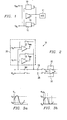
- a voiceband CODEC 18 having an improved sigma-delta A/D converter in accordance with the present invention is shown in Figure 2.
- the incoming signal ⁇ in is connected to the comparators C p 24 and C n 22 (which can be designed for very low current since speed and offset are not a primary concern), as well.
- Threshold voltages, V p and V n (which can be generated from the bandgap or derived from the supply voltage through a resistor/diode division), are coupled to comparators, C p 24 and C n 22, respectively.
- the incoming signal is sensed by comparators C p and C n , comparing the incoming signal with voltages V p and V n .
- Comparators C p and C n are connected to switches, sw p and sw n , respectively for switching in voltage levels, V p and V n , respectively. All three switches, sw 1 , sw p and sw n , couple to a sigma-delta ADC 34. Switch sw 1 couples to receive the incoming signal ⁇ in .
- switch sw 1 In operation, when incoming signal ⁇ in rises above the threshold voltage V p , switch sw 1 opens and comparator C p turns on, closing switch sw p . Accordingly, the fixed voltage V p is supplied to the sigma delta ADC 34. When the value of the signal goes below the threshold voltage, comparator C p shuts off, opening switch sw p . Simultaneously, switch sw 1 closes and incoming signal ⁇ in is supplied directly to sigma-DAC 34.
- switch sw 1 When incoming signal ⁇ in goes below threshold voltage V n , switch sw 1 opens and comparator C n turns on, closing switch sw n . Accordingly, the fixed voltage V n is supplied to the sigma delta ADC 34. When the value of signal ⁇ in rises above the threshold voltage V n , the comparator C n shuts off, opening switch sw n . Simultaneously, switch sw 1 closes and incoming signal ⁇ in is supplied directly to the sigma delta ADC.
- Figure 3a displays the input signal ⁇ in
- Figure 3b shows the clipped input signal ⁇ clip seen by the sigma-delta ADC 34.
- switch sw 1 opens and comparator C p turns on, closing switch sw p .
- the voltage ⁇ clip is equal to the threshold voltage V p .
- the comparator C p shuts off, opening switch sw p .
- Switch sw 1 closes and, as a result, voltage ⁇ clip equals the incoming signal ⁇ in .
- switch sw 1 opens and the comparator C n turns on, closing switch sw n . Accordingly, voltage ⁇ clip equals the fixed voltage V n .
- the signal clipping circuit for switched capacitor sigma delta analog-to-digital converter (ADC) of the present invention can be used in a variety of telecommunication and other applications.
- the signal clipping circuit for improved sigma delta analog-to-digital converters can be implemented in wireless user terminals and base stations operating according to international standards, such as for example CDMA (Code Division Multiple Access) and GSM (Global System for Mobile Communication).
- FIG. 4 illustrates a wireless communication system in which the signal clipping circuit for improved sigma delta analog-to-digital converters of the present invention may be implemented.
- Wireless communication system 40 comprises a wireless user terminal (a cellular handset being illustrated) 42 that communicates with a base station (a cellular base station being illustrated) 44 over an uplink channel 46 and downlink channel 48.
- the base station and the wireless user terminal unit operate in a similar manner.
- Time Domain Duplex the communication between wireless user terminal 42 and base station 44 is on a single channel. Much like a walky-talky, the channel is shared in time by the mobile station transmitter and the base station transmitter. A time slot is dedicated to the uplink and another timeslot is dedicated to a downlink. The relative length of the uplink and downlink time slots can be adjusted to accommodate asymmetric data traffic. If it is found that downlink data traffic is on average twice that of uplink, then the downlink time slot is twice as long as the uplink time slot.
- Frequency Domain Duplex the wireless user terminal 42 and the base station 44 communicate over a pair of radio frequencies.
- the lower frequency is the uplink during which the mobile station sends information to the base station.
- Both uplink and downlink are each composed of a signal source, a transmitter, the propagation path, a receiver and a method of presenting the information.
- Both wireless user terminal and base station embody the invention with transmitters, which convert digital data to analog signals at high speed and with high resolution.
- the base station could convert the entire multi-carrier downlink signal to analog for use in a single RF transmitter.
- the wireless user terminal is explained in the following.
- FIG. 5 presents a top-level block diagram 50 of the wireless user terminal 42.
- radio frequency (RF) signals are received and transmitted by the RF section 52.
- RF section 52 comprises a duplexer 76 coupling an antenna 78 to a receiver 68 and a power amplifier 74.
- a modulator 72 is coupled to power amplifier 74 and to a synthesizer 70.
- Synthesizer 70 is further coupled to receiver 68.
- RF section 52 is further coupled to an analog baseband 54.
- analog baseband 54 comprises an RF interface 56 and an audio interface 58.
- a speaker 88 and a microphone 90 are coupled to audio interface 58.
- RF interface 56 is coupled to both receiver 68 and modulator 72 of RF section 52.
- the analog RF interface 56 includes I and Q analog-to-digital converters (ADCs), according to the present invention, and digital-to-analog converters (DACs), for conversion between the analog and digital domains.
- Audio interface 58 may also include I and Q analog-to-digital converters (ADCs), according to an embodiment of the present invention, and digital-to-analog converters (DACs), for conversion between the digital and analog domains.
- Analog baseband 54 is further coupled to a digital baseband 60.
- digital baseband 60 comprises three elements: digital signal processor (DSP) 62, microcontroller unit (MCU) 64 and application specific integrated circuit (ASIC) 66.
- DSP 62 couples audio interface 54 to RF interface 56 and to microcontroller unit (MCU) 64.
- Digital signal processor (DSP) 62 and microcontroller unit (MCU) 64 are further coupled to ASIC backplane 66.
- Microcontroller unit (MCU) 64 is further coupled to a user interface 80, which comprises at least a user display 82 and a keyboard 84 (an optional SIM card 86 is also disclosed).
- the digital signal processor (DSP) 62 provides programmable speech coding and decoding (vocoder), channel coding and decoding, equalization, demodulation and encryption.
- the microcontroller unit (MCU) handles level 2 & 3 protocol, radio resource management, short message services, man-machine interface and the real-time operating system.
- the ASIC backplane 66 performs all chip-rate processing. While top level diagram 50 illustrates RF section 52, analog baseband 54 and digital baseband 60 as being separate packages or chips, the invention contemplates substitution of any of the above with an equivalent function, such as an RF function, and/or an analog baseband function and/or a digital baseband function. The functions will remain the same even if the actual implementation varies.
- the invention further contemplates that RF section 52, analog baseband 54 and digital baseband 60 may be selectively combined and/or integrated into one or two packages or chips.
- An uplink voice processing chain 46 for a wireless user terminal 42 is illustrated in Figure 6.
- This channel includes a CODEC 100 coupling a microphone 90 to a vocoder 98, a baseband modulator 96 coupling vocoder 98 to a digital-to-analog converter 92 at high speed and high resolution.
- An RF transmitter 94 (part of RF section 52) couples an antenna 78 to digital-to-analog converter 92.
- modulator 72 is implemented as two RF mixers, I and Q driven by the synthesizer, implemented as an RF local oscillator.
- RF transmitter CODEC 100 includes an audio amplifier (not shown), sigma-delta analog-to-digital converter (ADC) (not shown) and a digital filter (not shown) coupled together on one chip.
- the CODEC receives an analog voice signal through the microphone and converts it to a digital signal. While CODEC 100 is shown as being separate from digital baseband 60, it may also be internal to digital baseband 60.
- CODEC 100 transcodes audio signals into digital words using the algorithms contained in the VOCODER. This signal is then complex modulated, converted to analog (I&Q) and applied to the transmitter.
- the transmitter is complex modulated at the radio frequency assigned to the handset. It uses a power amplifier coupled to the antenna 78 to transmit the digital signal, effectively communicating the (digital) voice information to the base station receiver.
- a downlink voice channel 48 for wireless user terminal 42 is illustrated in Figure 7.
- This channel includes an RF receiver 102 (part of RF section 52) coupling antenna 78 to an analog-to-digital converter (ADC) 104, according to the invention, a vocoder 98 coupling a demodulator 96 to a CODEC 100, and a speaker 88 coupled to CODEC 100.
- CODEC 100 is shown as being separate from digital baseband 60, it may also be internal to digital baseband 60.
- CODEC 100 transcodes the digital words into analog signals using the algorithms contained in the VOCODER.
- CODEC 100 includes a digital filter, DAC and audio amplifier coupled together on one chip.
- the RF receiver uses an AGC circuit which varies the IF amplifier gain as a function of the received signal. The goal is to present the analog-to-digital converters (ADCs) with a full-scale analog signal without distortion and with minimal noise.
- ADC analog-to-digital converter
- the band structure of the cellular system in which the communication system of the present invention operates is composed of tightly packed RF carriers with very high spectral density.
- the world's most widely deployed TDMA system is GSM, where the GMSK-modulated carriers are placed on a 200-Khz raster 106 with adjacent channel signal interference suppressed to -30dBc at the first adjacent channel and -60dBc at the second.
- the 2-G CDMA system used in America (IS-95) uses QPSK-modulated (at 1.2288 Msps) carriers spaced at 1.25 Mhz 108 with very little guard band. Each carrier can be modulated with up to 32 Walsh codes, which are used to separate the users.
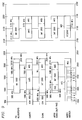
- Figure 9 illustrates the spectral definition of the 2G and 3G cellular regulations.
- the base station transmitter operates on the upper frequency band. For example, in Europe the base station receives from 1900 to 1980 Mhz and transmits from 2110 to 2170 Mhz.
- the signal analog-to-digital converter of the present invention can be use in other applications, such as data communication systems, hard disk drives, cd players, video displays, and any other application where there is a large amount of data that must be converted quickly.
Landscapes
- Engineering & Computer Science (AREA)
- Theoretical Computer Science (AREA)
- Compression, Expansion, Code Conversion, And Decoders (AREA)
- Analogue/Digital Conversion (AREA)
Abstract
Description
Initially, the audio CODEC receives an analog voice signal through the microphone and converts it to a digital signal. The digital signal is forwarded to a digital signal processor for processing. This signal is transmitted to a receiver. In the receiver, the digital signal is processed through the digital signal processor and forwarded to a D/A converter. The analog signal is fed to a speaker.
Claims (7)
- A wireless user terminal having radio frequency (RF) communication capability, comprising:a digital baseband;an RF section;an analog baseband coupling said digital baseband to said RF section, wherein said analog baseband further comprises:a switch having a first lead coupled to an input and a second lead coupled to an analog-to-digital converter (ADC);a signal clipping circuit having a first input coupled to said first input of said switch, a second input coupled to receive a first reference voltage, a third input coupled to receive a second reference voltage, and an output coupled to said second lead of said switch.
- The wireless user terminal of claim 1 wherein said analog-to-digital converter is a sigma-delta analog-to-digital converter.
- The wireless user terminal of claim 1 or 2 wherein said digital baseband further comprises:a digital signal processor (DSP);a microcontroller unit (MCU) coupled to said DSP; andan ASIC backplane coupled to said DSP and said MCU.
- The wireless user terminal of claim 1, 2 or 3 wherein the clipping circuit comprises a first branch for clipping an output signal at an upper boundary, and a second branch for clipping the output signal at a lower boundary.
- The wireless user terminal claim 4 wherein the first branch comprises:a comparator having an output, a first input coupled to receive a first threshold voltage and a second input coupled to receive the input signal; anda switch coupled to the output of the comparator, the output voltage of the comparator couples to the switch to open and close the switch.
- The wireless user terminal of claim 4 wherein the second branch comprises:a comparator having an output, a first input coupled to receive a first threshold voltage and a second input coupled to receive the input signal; anda switch coupled to the output of the comparator, the output voltage of the comparator couples to the switch to open and close the switch.
- A radio frequency (RF) enabled communications system, comprising:a base station; anda wireless user terminal capable of communicating with said base station via radio frequency (RF) communication and as claimed in any preceding claim.
Applications Claiming Priority (2)
| Application Number | Priority Date | Filing Date | Title |
|---|---|---|---|
| US846841 | 2001-04-30 | ||
| US09/846,841 US6882861B2 (en) | 2001-04-30 | 2001-04-30 | Wireless user terminal and system having signal clipping circuit for switched capacitor sigma delta analog to digital converters |
Publications (2)
| Publication Number | Publication Date |
|---|---|
| EP1257061A2 true EP1257061A2 (en) | 2002-11-13 |
| EP1257061A3 EP1257061A3 (en) | 2004-03-17 |
Family
ID=25299089
Family Applications (1)
| Application Number | Title | Priority Date | Filing Date |
|---|---|---|---|
| EP02100428A Ceased EP1257061A3 (en) | 2001-04-30 | 2002-04-30 | Wireless user terminal and system having signal clipping circuit for switched capacitor sigma delta analog to digital converters |
Country Status (3)
| Country | Link |
|---|---|
| US (1) | US6882861B2 (en) |
| EP (1) | EP1257061A3 (en) |
| JP (1) | JP2002368616A (en) |
Families Citing this family (17)
| Publication number | Priority date | Publication date | Assignee | Title |
|---|---|---|---|---|
| US7110726B1 (en) * | 2003-05-22 | 2006-09-19 | Quake Global, Inc. | RF ASIC for subscriber communicator |
| DE10342056B4 (en) * | 2003-09-11 | 2005-11-10 | Infineon Technologies Ag | Addition circuit for sigma-delta modulator circuits |
| US7542505B2 (en) * | 2003-10-20 | 2009-06-02 | Northrop Grumman Corporation | Systems and methods for signal conversion |
| US7079058B2 (en) * | 2004-05-18 | 2006-07-18 | Broadcom Corporation | Powering down of DAC and ADC for receive/transmit modes of operation in a wireless device |
| US7751784B2 (en) * | 2004-06-30 | 2010-07-06 | Black Sand Technologies, Inc. | Method of protecting power amplifiers |
| US7751783B2 (en) * | 2004-06-30 | 2010-07-06 | Black Sand Technologies, Inc. | Power amplifier protection circuit and associated methods |
| KR100766073B1 (en) | 2005-12-06 | 2007-10-11 | 한국전자통신연구원 | Multi-bit Sigma Delta Modulator with One DAC Capacitor and Digital-Analog Convertor for Multi-bit Sigma Delta Modulator |
| US7388533B2 (en) | 2005-12-06 | 2008-06-17 | Electronics And Telecommunications Research Institute | Multi-bit sigma-delta modulator and digital-to-analog converter with one digital-to-analog capacitor |
| US20080075307A1 (en) * | 2006-01-30 | 2008-03-27 | Penton Audio Usa | Digital Signal Processing Amplifier |
| US8553720B2 (en) * | 2006-04-19 | 2013-10-08 | Marvell World Trade Ltd. | Adaptive speed control for MAC-PHY interfaces |
| US8374225B2 (en) * | 2006-12-19 | 2013-02-12 | Broadcom Corporation | Voice/data/RF integrated circuit |
| US7697899B2 (en) * | 2006-08-31 | 2010-04-13 | Broadcom Corporation | RFIC with on-chip acoustic transducer circuit |
| DE102007018613A1 (en) * | 2007-04-19 | 2008-10-23 | Xignal Technologies Ag | Circuit arrangement and method for signal voltage limiting |
| US8947207B2 (en) | 2008-04-29 | 2015-02-03 | Quake Global, Inc. | Method and apparatus for a deployable radio-frequency identification portal system |
| KR20100133748A (en) * | 2009-06-12 | 2010-12-22 | 삼성전자주식회사 | Discrete time filter and receiver containing it |
| US9841492B2 (en) | 2013-02-25 | 2017-12-12 | Quake Global, Inc. | Ceiling-mounted RFID-enabled tracking |
| JP6280571B2 (en) | 2013-02-26 | 2018-02-14 | クエイク グローバル インコーポレイティッドQuake Global, Inc. | Method and apparatus for automatic identification wristband |
Family Cites Families (15)
| Publication number | Priority date | Publication date | Assignee | Title |
|---|---|---|---|---|
| US3704363A (en) * | 1971-06-09 | 1972-11-28 | Ibm | Statistical and environmental data logging system for data processing storage subsystem |
| CA1184660A (en) | 1981-06-12 | 1985-03-26 | Robert W. Harris | Enhanced delta modulation encoder |
| US4877981A (en) * | 1988-05-25 | 1989-10-31 | Ampex Corporation | Precision device for soft clipping AC and DC signals |
| US5166936A (en) * | 1990-07-20 | 1992-11-24 | Compaq Computer Corporation | Automatic hard disk bad sector remapping |
| CN1097353C (en) | 1994-09-14 | 2002-12-25 | 艾利森公司 | Satellite Communications Adapter for Cellular Handsets |
| SE9403337L (en) | 1994-10-03 | 1995-11-27 | Ericsson Telefon Ab L M | Method and apparatus for obtaining a wide dynamic range of a receiver in a digital radio transmission system |
| KR0111811Y1 (en) * | 1994-12-30 | 1998-10-01 | 이형도 | Voltage clipper circuit |
| US5758057A (en) * | 1995-06-21 | 1998-05-26 | Mitsubishi Denki Kabushiki Kaisha | Multi-media storage system |
| US5661422A (en) | 1995-12-12 | 1997-08-26 | Analog Devices, Inc. | High speed saturation prevention for saturable circuit elements |
| US5914967A (en) * | 1997-01-18 | 1999-06-22 | Hitachi Computer Products (America), Inc. | Method and apparatus for protecting disk drive failure |
| US6167485A (en) * | 1997-12-31 | 2000-12-26 | Emc Corporation | On-line data verification and repair in redundant storage systems |
| US6229470B1 (en) * | 1998-07-28 | 2001-05-08 | Texas Instruments Incorporated | Analog clipping circuit for mixed signal codecs |
| US6084467A (en) * | 1998-10-30 | 2000-07-04 | Texas Instruments Incorporated | Analog amplifier clipping circuit |
| US6476745B1 (en) * | 1998-11-25 | 2002-11-05 | Texas Instruments Incorporated | Voice codec automatic gain control |
| US6424280B2 (en) * | 2000-01-21 | 2002-07-23 | Texas Instruments Incorporated | Signal clipping circuit for switched capacitor sigma delta analog to digital converters |
-
2001
- 2001-04-30 US US09/846,841 patent/US6882861B2/en not_active Expired - Lifetime
-
2002
- 2002-04-30 EP EP02100428A patent/EP1257061A3/en not_active Ceased
- 2002-04-30 JP JP2002128455A patent/JP2002368616A/en active Pending
Also Published As
| Publication number | Publication date |
|---|---|
| US20020160732A1 (en) | 2002-10-31 |
| JP2002368616A (en) | 2002-12-20 |
| US6882861B2 (en) | 2005-04-19 |
| EP1257061A3 (en) | 2004-03-17 |
Similar Documents
| Publication | Publication Date | Title |
|---|---|---|
| US6882861B2 (en) | Wireless user terminal and system having signal clipping circuit for switched capacitor sigma delta analog to digital converters | |
| US20050118977A1 (en) | Method, apparatus, and systems for digital radio communication systems | |
| US7110732B2 (en) | Subsampling RF receiver architecture | |
| RU2144256C1 (en) | Power amplifier with double operational mode | |
| JP5031847B2 (en) | Digital linear transmitter architecture | |
| US7023267B2 (en) | Switching power amplifier using a frequency translating delta sigma modulator | |
| JP2004526337A (en) | Dual mode communication transmitter | |
| JP2008509575A (en) | All-digital transmitter including digital bandpass sigma-delta modulator | |
| EP1107462B1 (en) | Digital-to-analog converter with sigma delta conversion and storage | |
| US5884189A (en) | Multiple-modes adaptable radiotelephone | |
| US6515605B2 (en) | Base station having high speed, high resolution, digital-to-analog converter with off-line sigma delta conversion and storage | |
| JPH06350484A (en) | Dual mode amplifier network | |
| US6489908B2 (en) | Wireless local loop terminal and system having high speed, high resolution, digital-to-analog converter with off-line sigma-delta conversion and storage | |
| Vankka et al. | A GSM/EDGE/WCDMA modulator with on-chip D/A converter for base station | |
| US7020219B2 (en) | Wireless user terminal and system having high speed, high resolution, digital-to-analog converter with off-line sigma delta conversion and storage | |
| US20030202616A1 (en) | Radio receiver utilizing a single analog to digital converter | |
| KR100751999B1 (en) | RF signal generation method and device | |
| US6424280B2 (en) | Signal clipping circuit for switched capacitor sigma delta analog to digital converters | |
| Schultes et al. | DECT transceiver architectures: Superheterodyne or direct conversion? | |
| WO2004098080A1 (en) | Analog front end for a digital dual-band intermediate frequency sampling receiver | |
| US20050168268A1 (en) | Transmitter IF section and method enabling IF output signal amplitude that is less sensitive to process, voltage, and temperature | |
| US20070286115A1 (en) | Radio device and control method therefor | |
| EP1130785A2 (en) | Signal clipping circuit for switched capacitor sigma delta analog to digital converters | |
| Efstathiou et al. | Enabling components for multi-standard software radio base stations | |
| CN108242937B (en) | Multi-rate energy efficient Delta-sigma converter |
Legal Events
| Date | Code | Title | Description |
|---|---|---|---|
| PUAI | Public reference made under article 153(3) epc to a published international application that has entered the european phase |
Free format text: ORIGINAL CODE: 0009012 |
|
| AK | Designated contracting states |
Kind code of ref document: A2 Designated state(s): AT BE CH CY DE DK ES FI FR GB GR IE IT LI LU MC NL PT SE TR |
|
| AX | Request for extension of the european patent |
Free format text: AL;LT;LV;MK;RO;SI |
|
| RIN1 | Information on inventor provided before grant (corrected) |
Inventor name: SADKOWSKI, ROBERTO Inventor name: PANASIK, CARL |
|
| PUAL | Search report despatched |
Free format text: ORIGINAL CODE: 0009013 |
|
| AK | Designated contracting states |
Kind code of ref document: A3 Designated state(s): AT BE CH CY DE DK ES FI FR GB GR IE IT LI LU MC NL PT SE TR |
|
| AX | Request for extension of the european patent |
Extension state: AL LT LV MK RO SI |
|
| RIC1 | Information provided on ipc code assigned before grant |
Ipc: 7H 03M 1/12 B Ipc: 7H 03M 3/02 A |
|
| 17P | Request for examination filed |
Effective date: 20040917 |
|
| AKX | Designation fees paid |
Designated state(s): DE FR GB |
|
| 17Q | First examination report despatched |
Effective date: 20050302 |
|
| STAA | Information on the status of an ep patent application or granted ep patent |
Free format text: STATUS: THE APPLICATION HAS BEEN REFUSED |
|
| 18R | Application refused |
Effective date: 20060620 |