EP1256925A2 - Display panel drive apparatus - Google Patents
Display panel drive apparatus Download PDFInfo
- Publication number
- EP1256925A2 EP1256925A2 EP02009359A EP02009359A EP1256925A2 EP 1256925 A2 EP1256925 A2 EP 1256925A2 EP 02009359 A EP02009359 A EP 02009359A EP 02009359 A EP02009359 A EP 02009359A EP 1256925 A2 EP1256925 A2 EP 1256925A2
- Authority
- EP
- European Patent Office
- Prior art keywords
- row electrode
- drive
- drivers
- row
- circuit
- Prior art date
- Legal status (The legal status is an assumption and is not a legal conclusion. Google has not performed a legal analysis and makes no representation as to the accuracy of the status listed.)
- Withdrawn
Links
Images



Classifications
-
- G—PHYSICS
- G09—EDUCATION; CRYPTOGRAPHY; DISPLAY; ADVERTISING; SEALS
- G09G—ARRANGEMENTS OR CIRCUITS FOR CONTROL OF INDICATING DEVICES USING STATIC MEANS TO PRESENT VARIABLE INFORMATION
- G09G3/00—Control arrangements or circuits, of interest only in connection with visual indicators other than cathode-ray tubes
- G09G3/20—Control arrangements or circuits, of interest only in connection with visual indicators other than cathode-ray tubes for presentation of an assembly of a number of characters, e.g. a page, by composing the assembly by combination of individual elements arranged in a matrix no fixed position being assigned to or needed to be assigned to the individual characters or partial characters
- G09G3/22—Control arrangements or circuits, of interest only in connection with visual indicators other than cathode-ray tubes for presentation of an assembly of a number of characters, e.g. a page, by composing the assembly by combination of individual elements arranged in a matrix no fixed position being assigned to or needed to be assigned to the individual characters or partial characters using controlled light sources
- G09G3/28—Control arrangements or circuits, of interest only in connection with visual indicators other than cathode-ray tubes for presentation of an assembly of a number of characters, e.g. a page, by composing the assembly by combination of individual elements arranged in a matrix no fixed position being assigned to or needed to be assigned to the individual characters or partial characters using controlled light sources using luminous gas-discharge panels, e.g. plasma panels
- G09G3/288—Control arrangements or circuits, of interest only in connection with visual indicators other than cathode-ray tubes for presentation of an assembly of a number of characters, e.g. a page, by composing the assembly by combination of individual elements arranged in a matrix no fixed position being assigned to or needed to be assigned to the individual characters or partial characters using controlled light sources using luminous gas-discharge panels, e.g. plasma panels using AC panels
- G09G3/296—Driving circuits for producing the waveforms applied to the driving electrodes
-
- G—PHYSICS
- G09—EDUCATION; CRYPTOGRAPHY; DISPLAY; ADVERTISING; SEALS
- G09G—ARRANGEMENTS OR CIRCUITS FOR CONTROL OF INDICATING DEVICES USING STATIC MEANS TO PRESENT VARIABLE INFORMATION
- G09G3/00—Control arrangements or circuits, of interest only in connection with visual indicators other than cathode-ray tubes
- G09G3/20—Control arrangements or circuits, of interest only in connection with visual indicators other than cathode-ray tubes for presentation of an assembly of a number of characters, e.g. a page, by composing the assembly by combination of individual elements arranged in a matrix no fixed position being assigned to or needed to be assigned to the individual characters or partial characters
- G09G3/22—Control arrangements or circuits, of interest only in connection with visual indicators other than cathode-ray tubes for presentation of an assembly of a number of characters, e.g. a page, by composing the assembly by combination of individual elements arranged in a matrix no fixed position being assigned to or needed to be assigned to the individual characters or partial characters using controlled light sources
- G09G3/28—Control arrangements or circuits, of interest only in connection with visual indicators other than cathode-ray tubes for presentation of an assembly of a number of characters, e.g. a page, by composing the assembly by combination of individual elements arranged in a matrix no fixed position being assigned to or needed to be assigned to the individual characters or partial characters using controlled light sources using luminous gas-discharge panels, e.g. plasma panels
- G09G3/288—Control arrangements or circuits, of interest only in connection with visual indicators other than cathode-ray tubes for presentation of an assembly of a number of characters, e.g. a page, by composing the assembly by combination of individual elements arranged in a matrix no fixed position being assigned to or needed to be assigned to the individual characters or partial characters using controlled light sources using luminous gas-discharge panels, e.g. plasma panels using AC panels
- G09G3/291—Control arrangements or circuits, of interest only in connection with visual indicators other than cathode-ray tubes for presentation of an assembly of a number of characters, e.g. a page, by composing the assembly by combination of individual elements arranged in a matrix no fixed position being assigned to or needed to be assigned to the individual characters or partial characters using controlled light sources using luminous gas-discharge panels, e.g. plasma panels using AC panels controlling the gas discharge to control a cell condition, e.g. by means of specific pulse shapes
- G09G3/294—Control arrangements or circuits, of interest only in connection with visual indicators other than cathode-ray tubes for presentation of an assembly of a number of characters, e.g. a page, by composing the assembly by combination of individual elements arranged in a matrix no fixed position being assigned to or needed to be assigned to the individual characters or partial characters using controlled light sources using luminous gas-discharge panels, e.g. plasma panels using AC panels controlling the gas discharge to control a cell condition, e.g. by means of specific pulse shapes for lighting or sustain discharge
-
- G—PHYSICS
- G09—EDUCATION; CRYPTOGRAPHY; DISPLAY; ADVERTISING; SEALS
- G09G—ARRANGEMENTS OR CIRCUITS FOR CONTROL OF INDICATING DEVICES USING STATIC MEANS TO PRESENT VARIABLE INFORMATION
- G09G2310/00—Command of the display device
- G09G2310/02—Addressing, scanning or driving the display screen or processing steps related thereto
- G09G2310/0202—Addressing of scan or signal lines
- G09G2310/0218—Addressing of scan or signal lines with collection of electrodes in groups for n-dimensional addressing
-
- G—PHYSICS
- G09—EDUCATION; CRYPTOGRAPHY; DISPLAY; ADVERTISING; SEALS
- G09G—ARRANGEMENTS OR CIRCUITS FOR CONTROL OF INDICATING DEVICES USING STATIC MEANS TO PRESENT VARIABLE INFORMATION
- G09G2320/00—Control of display operating conditions
- G09G2320/06—Adjustment of display parameters
- G09G2320/0606—Manual adjustment
-
- G—PHYSICS
- G09—EDUCATION; CRYPTOGRAPHY; DISPLAY; ADVERTISING; SEALS
- G09G—ARRANGEMENTS OR CIRCUITS FOR CONTROL OF INDICATING DEVICES USING STATIC MEANS TO PRESENT VARIABLE INFORMATION
- G09G2320/00—Control of display operating conditions
- G09G2320/06—Adjustment of display parameters
- G09G2320/066—Adjustment of display parameters for control of contrast
-
- G—PHYSICS
- G09—EDUCATION; CRYPTOGRAPHY; DISPLAY; ADVERTISING; SEALS
- G09G—ARRANGEMENTS OR CIRCUITS FOR CONTROL OF INDICATING DEVICES USING STATIC MEANS TO PRESENT VARIABLE INFORMATION
- G09G2330/00—Aspects of power supply; Aspects of display protection and defect management
- G09G2330/04—Display protection
-
- G—PHYSICS
- G09—EDUCATION; CRYPTOGRAPHY; DISPLAY; ADVERTISING; SEALS
- G09G—ARRANGEMENTS OR CIRCUITS FOR CONTROL OF INDICATING DEVICES USING STATIC MEANS TO PRESENT VARIABLE INFORMATION
- G09G3/00—Control arrangements or circuits, of interest only in connection with visual indicators other than cathode-ray tubes
- G09G3/20—Control arrangements or circuits, of interest only in connection with visual indicators other than cathode-ray tubes for presentation of an assembly of a number of characters, e.g. a page, by composing the assembly by combination of individual elements arranged in a matrix no fixed position being assigned to or needed to be assigned to the individual characters or partial characters
- G09G3/22—Control arrangements or circuits, of interest only in connection with visual indicators other than cathode-ray tubes for presentation of an assembly of a number of characters, e.g. a page, by composing the assembly by combination of individual elements arranged in a matrix no fixed position being assigned to or needed to be assigned to the individual characters or partial characters using controlled light sources
- G09G3/28—Control arrangements or circuits, of interest only in connection with visual indicators other than cathode-ray tubes for presentation of an assembly of a number of characters, e.g. a page, by composing the assembly by combination of individual elements arranged in a matrix no fixed position being assigned to or needed to be assigned to the individual characters or partial characters using controlled light sources using luminous gas-discharge panels, e.g. plasma panels
- G09G3/288—Control arrangements or circuits, of interest only in connection with visual indicators other than cathode-ray tubes for presentation of an assembly of a number of characters, e.g. a page, by composing the assembly by combination of individual elements arranged in a matrix no fixed position being assigned to or needed to be assigned to the individual characters or partial characters using controlled light sources using luminous gas-discharge panels, e.g. plasma panels using AC panels
- G09G3/296—Driving circuits for producing the waveforms applied to the driving electrodes
- G09G3/2965—Driving circuits for producing the waveforms applied to the driving electrodes using inductors for energy recovery
Definitions
- the present invention relates to a drive apparatus for a display panel such as a matrix display-type plasma display panel (PDP).
- a display panel such as a matrix display-type plasma display panel (PDP).
- PDP plasma display panel
- PDP is a thin, flat display for which various kinds of research have been conducted, and that one kind of PDP is known as a matrix display-type PDP.
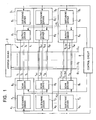
- Fig. 1 shows a schematic configuration of a PDP drive apparatus having the PDP.
- a PDP 1 has row electrodes Y 1 to Y nk and row electrodes X 1 to X nk forming row electrode pairs such that each X and Y pair corresponds to each row (row 1 to row nk) of a single screen.
- the PDP 1 additionally comprises column electrodes D 1 to D m constituting column electrodes that correspond to each column (column 1 to column m) of a single screen.
- the column electrodes D 1 to D m are formed orthogonally to the row electrode pairs with dielectric layers and a discharge gap, which are not shown in the figure, interposed therebetween.
- a discharge cell that corresponds to a single pixel is formed at the intersection of one row electrode pair and one column electrode.
- the row electrodes X 1 to X nk and row electrodes Y 1 to Y nk are each divided into n groups of k rows per group. Specifically, these groups are X 1 to X k , X k+1 to X 2k , ..., X (n-1)k+1 to X nk and Y 1 to Y k , Y k+1 to Y 2k , ..., Y (n-1)k+1 to Y nk . These n groups correspond to X row electrode drivers 3 1 to 3 n and Y row electrode drivers 4 1 to 4 n , respectively.
- a address driver 2 converts pixel data of each pixel based on a video signal to a pixel data pulse having a voltage value corresponding to a logic level of the pixel data and applies the voltage to each of the column electrodes D 1 to D m for each row.
- the X row electrode drivers 3 1 to 3 n respectively, have sustaining drivers 5 1 to 5 n and output drivers 6 1 to 6 n . There is a line XL commonly connecting between sustaining drivers 5 1 to 5 n and output drivers 6 1 to 6 n .
- Each of the sustaining drivers 5 1 to 5 n generates, as a drive pulse, a reset pulse for initializing residual wall charge of each discharge cell and a sustaining discharge pulse for sustaining a discharge luminescence state of a luminescent discharge cell as described later, and applies these pulses to the row electrodes X 1 to X nk via the corresponding output driver 61 to 6 n .
- the Y row electrode drivers 4 1 to 4 n respectively, have sustaining drivers 7 1 to 7 n and scan drivers 8 1 to 8 n . There is a line YL commonly connecting between the sustaining drivers 7 1 to 7 n and the scan drivers 8 1 to 8 n .
- Each of the sustaining drivers 7 1 to 7 n in a manner similar to the sustaining drivers 5 1 to 5 n of the X row electrode drivers 3 1 to 3 n , generates a reset pulse for initializing residual wall charge of each discharge cell and a sustaining discharge pulse for sustaining a discharge luminescence state of each luminescent discharge cell, and applies these pulses on each of the row electrodes Y 1 to Y nk via the corresponding scan driver 8 1 to 8 n .
- Each of the scan drivers 8 1 to 8 n generates a scan pulse SP for setting a luminescent discharge cell or non-luminescent discharge cell by obtaining the charge corresponding to the pixel data pulse for each discharge cell, and applies the pulse to the row electrodes Y 1 to Y nk .
- the connecting lines XL and YL are provided to unify the voltage levels of the drive pulses for the drivers 3 1 to 3 n , 4 1 to 4 n , respectively.
- a control circuit 9 controls generation timing of the drive pulses of sustaining drivers 5 1 to 5 n , output drivers 6 1 to 6 n , the sustaining drivers 7 1 to 7 n , and the scan drivers 8 1 to 8 n .
- Fig. 2 shows the configurations of the sustaining driver 7 1 and the scan driver 8 1 .
- the sustaining driver 7 1 has power supplies B1, B2, a capacitor C, coils L1 to L2, a resistor R1, diodes D1, D2, and switching elements S1 to S6.
- the power supply B1 outputs a voltage V R .
- the power supply B2 outputs a voltage V S .
- the negative terminal of the power supply B1 is grounded, and the positive terminal is connected to the above-mentioned connecting line YL via the switching element S6 and the resistor R1.
- the connecting line YL is grounded via the switching element S5 and the switching element S4.
- the voltage V S from the positive terminal of the power supply B2 is applied via the switching element S3 to a connecting line CL between the switching element S5 and the switching element S4.
- the switching element S1, the diode D1, the coil L1, and the capacitor C are connected in series sequentially from the connecting line CL side.
- the polarity of the diode D1 is such that the anode is the coil L1 side and the cathode is the switching element S1 side.
- the series circuit including the coil L2, diode D2, and switching element S2 is connected in parallel to the series portion including the switching element S1, diode D1, and coil L1.
- One end of the coil L2 is connected to the connecting line CL, and one end of the switching element S2 is connected to the capacitor C.
- the polarity of the diode D2 is such that the anode is the coil L2 side and the cathode is the switching element S2 side.
- the scan driver 81 has a power supply B3, switching elements S7 1 to S7 k , S8 1 to S8 k , and diodes D7 1 to D7 k , D8 1 to D8 k .
- the power supply B3 outputs a voltage V h .
- the positive terminal of the power supply B3 is connected to the connecting line YL, and the negative terminal is connected to a negative-side connecting line NL within the scan driver 8 1 .
- the switching elements S7 1 and S8 1 are connected in series, and the diodes D7 1 and D8 1 are also connected in series.
- the polarities of the diodes D7 1 and D8 1 are such that the cathode of the diode D7 1 is the connecting line YL side, the anode of the diode D7 1 and the cathode of the diode D8 1 are connected with each other, and the anode of diode D8 1 is the connecting line NL side.
- the connection point between the switching elements S7 1 and S8 1 and the connection point between the diodes D7 1 and D8 1 are connected with each other, and the connecting line between these connection points is connected to the row electrode Y 1 .
- the switching elements S7 2 , S8 2 , diodes D7 2 , D8 2 , and row electrode Y 2 ...
- the switching elements S7 k , S8 k , diodes D7 k , D8 k , and row electrode Y k are each connected in the same way as the switching elements S7 1 , S8 1 , diodes D7 1 , D8 1 , and row electrode Y 1 .
- the switching elements S1 to S6, S7 1 to S7 k , and S8 1 to S8 k are respectively switched in response to control signals supplied from a control circuit 9.
- the sustaining drivers 7 2 to 7 n and the sustaining drivers 5 1 to 5 n of the X row electrode drivers 3 1 to 3 n are also provided with the same configuration as the sustaining driver 7 1 .
- the power supply B1 is connected with the reverse polarity of that for the sustaining drivers 7 1 to 7 n .
- the scan drivers 8 2 to 8 n and the output drivers 6 1 to 6 n of the X row electrode drivers 3 1 to 3 n are also provided with the same configuration as the scan driver 8 1 .
- the operation of the PDP drive apparatus has a reset period, an address period, and a sustaining period.
- the sustaining drivers 5 1 to 5 n of the X row electrode drivers 3 1 to 3 n and the sustaining drivers 7 1 to 7 n of the Y row electrode drivers 4 1 to 4 n each generate reset pulses.
- the reset pulses are applied simultaneously to the row electrodes X 1 to X nk and row electrodes Y 1 to Y nk .
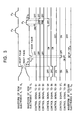
- Fig. 3 shows a negative reset pulse that is applied to the row electrode X 1 and a positive reset pulse that is applied to the row electrode Y 1 .
- the operation during the reset period is as follows.
- the switching element S6 is turned on, and the switching elements S1 to S5 are turned off.
- the switching elements S7 1 to S7 k are turned on, and the switching elements S8 1 to S8 k are turned off.
- an address period starts.
- the address driver 2 converts pixel data for each pixel based on a video signal to pixel data pulses DP 1 to DP m having voltage values corresponding to logic levels of the pixel data, and applies these voltages sequentially to the column electrodes D 1 to D m for each row.
- the pixel data pulses DP 1 to DP m are applied for the row electrode Y 1 as shown in Fig. 3.
- a scan pulse is repeatedly applied to the row electrodes Y 1 to Y nk in that order by the scan drivers 8 1 to 8 n in synchronism with the individual application timing of the pixel data pulses DP 1 to DP m .
- the operation during the address period will be explained as follows.
- the switching element S7 1 is turned off and the switching element S8 1 is turned on at the same time.
- a voltage -V h by the power supply B3 is added to the row electrode Y 1 , as shown in Fig. 3, to become a scan pulse.
- the ground potential of 0V is applied to the row electrode X 1 as shown in Fig. 3.
- the switching element S7 2 is turned off and the switching element S8 2 is turned on at the same time, and then the scan pulse is added to the row electrode Y 2 . In this manner, the scan pulse is applied sequentially to the row electrodes Y 1 to Y k .
- discharges will occur at discharge cells to which positive voltage pixel data pulses are respectively applied at the same time, and most of the wall charge as mentioned above is lost for each of the discharged cells. Since no discharge occurs at the remaining discharge cells to which a scan pulse is applied but no positive voltage pixel data pulse is applied, each wall charge remains.
- the discharge cells each of which has the wall charge are luminous discharge cells, and the discharged cells each of which has no wall charge are non-luminous discharge cells.
- the X row electrode drivers 3 1 to 3 n apply a positive voltage sustaining pulse IP X to the electrodes X 1 to X nk
- the Y row electrode drivers 4 1 to 4 n apply a sustaining pulse IP Y to the electrodes Y 1 to Y nk
- the application of the sustaining pulse IP X to the electrodes X 1 to X nk alternates with the application of the sustaining pulse IP y to the electrodes Y 1 to Y nk . Since luminous discharge cells each of which has the wall charge remained repeatedly emit, these cells maintain a luminous state.
- the switching element S1 is turned on and the switching element S4 is turned off during the sustain period.
- the potential of the electrode Y 1 is substantially equal to the ground potential of 0V when the switching element S4 is turned on.
- a current flows to the row element Y 1 via the coil L1, diode D1, switching element S1, switching element S5, connecting line YL, and switching element S7 1 due to a charge stored in the capacitor C, and charges the capacitance component between the row electrodes Y 1 and X 1 .
- the potential of the electrode Y 1 increases gradually as shown in Fig. 3 due to the time constant of the coil L2 and capacitance component.
- the switching element S1 is turned off and the switching element S3 is turned on.
- the voltage V S by the power supply B2 is applied to the row electrode Y 1 via the switching element S3, switching element S5, connecting line YL, and switching element S7 1 .
- the switching element S3 is turned off and the switching element S2 is turned on, and a current flows into the capacitor C via the diode D7 1 , connecting line YL, switching element S5, coil L2, diode D2, and switching element S2 from the electrode Y 1 due to the charge stored in the capacitance component between the row electrodes Y 1 and X 1 .
- the potential of the electrode Y 1 decreases gradually as shown in Fig.
- the switching element S2 is turned off and the switching element S4 is turned on.
- the row electrode Y 1 is supplied with the sustaining pulse IP y of a positive voltage as shown in Fig. 3, according to the operation.
- the row electrodes X 1 to X nk and row electrodes Y 1 to Y nk are each divided into n groups having k rows per group, and the X row electrode driver and Y row electrode driver are provided for each row electrode group as described above.
- the configuration is done to reduce a load for a single driver and distribute the overall generation of heat to each driver.
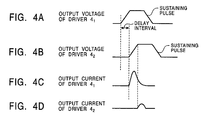
- the output current by the drive pulse of the Y row electrode driver 4 1 shown in Fig. 4C becomes larger than the output current by the drive pulse of the Y row electrode driver 4 2 shown in Fig. 4D, and the amount of heat generated by the Y row electrode driver 4 1 increases.
- An object of the present invention is to provide a drive apparatus for a display panel that can make power consumption of a row electrode drive circuit of each row electrode group substantially uniform to prevent an increase in the amount of heat generated therein.
- a drive apparatus for driving a display panel having a plurality of row electrode groups each including a plurality of row electrodes, and a plurality of column electrodes arrayed in the direction intersecting with each row electrode of the plurality of row electrode groups so as to form display cells at the intersection points; the drive apparatus further comprising: control means for generating a control signal for each of the row electrode groups; a row electrode drive circuit provided for each of the row electrode groups, for generating a drive pulse in response to the control signal and supplying the drive pulse to each row electrode of the corresponding row electrode group; and adjusting means for delaying the control signal which is supplied to the drive circuit for each of the row electrode groups.
- Fig. 5 shows the configuration of a PDP drive apparatus according to the present invention.
- the same symbols are used for the same parts as those used in the conventional apparatus shown in Fig. 1.
- delay circuits 10 1 to 10 n are respectively inserted between the control circuit 9 and the sustaining drivers 5 1 to 5 n of the X row electrode drivers 3 1 to 3 n , respectively, and delay circuits 11 1 to 11 n are similarly inserted between the control circuit 9 and the sustaining drivers 7 1 to 7 n of the Y row electrode drivers 4 1 to 4 n , respectively.
- control signals for switching the switching elements of the sustaining drivers 5 1 to 5 n are respectively supplied from the control circuit 9 to the sustaining drivers 5 1 to 5 n via the delay circuits 10 1 to 10 n .
- control signals for switching the switching elements of the sustaining drivers 7 1 to 7 n are respectively supplied from the control circuit 9 to the sustaining drivers 7 1 to 7 n via the delay circuits 11 1 to 11 n .
- the delay circuits 10 1 to 10 n and delay circuits 11 1 to 11 n are formed by integrating circuits having resistors Rx 1 to Rx n , Ry 1 to Ry n and capacitors Cx 1 to Cx n , Cy 1 to Cy n , respectively, as shown in Fig. 5.
- the resistors Rx 1 to Rx n and Ry 1 to Ry n are variable resistors, which can change the delay times of the delay circuits 10 1 to 10 n and delay circuits 11 1 to 11 n , respectively, in accordance with manual operation.
- the respective sustaining drivers can be activated at the same timing. Therefore, drive pulses (reset pulse pulses and sustaining pulses) can be generated at the same timing.
- the values of electric currents supplied to the row electrodes X 1 to X nk from the output drivers 6 1 to 6 n of the X row electrode drivers 3 1 to 3 n respectively, become substantially uniform, and similarly, the values of electric currents supplied to the row electrodes Y 1 to Y nk from the scan drivers 8 1 to 8 n of Y row electrode drivers 4 1 to 4 n , respectively, become substantially uniform. Heat generated in respective elements such as switching elements is distributed to each of the row electrode drivers 3 1 to 3 n , 4 1 to 4 n .
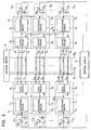
- Fig. 6 shows the configuration of a PDP drive apparatus of another embodiment of the present invention.
- the PDP drive apparatus of Fig. 6 has delay circuits 12 1 to 12 n , 13 1 to 13 n in a similar manner as those in the apparatus of Fig. 5.
- the sustaining drivers 5 1 to 5 n are modularized in a configuration including the delay circuits 12 1 to 12 n , respectively.
- the sustaining drivers 7 1 to 7 n are modularized in a configuration including the delay circuits 13 1 to 13 n , respectively.
- the delay circuits 12 1 to 12 n , 13 1 to 13 n are formed by integrating circuits including resistors R1x 1 to R1x n , R1y 1 to R1y n and capacitors C1x 1 to C1x n , C1y 1 to C1y n , respectively, as shown in Fig. 6.
- the resistors R1x 1 to R1x n , R1y 1 to R1y n and capacitors C1x 1 to C1x n , C1y 1 to C1y n have positive temperature characteristics.
- the resistance value, for example, of the delay circuit within that sustaining driver increases for generating heat, and the delay time of the delay circuit becomes longer.
- the respective sustaining drivers switching elements S1 to S6 can be activated at the same timing. Therefore, drive pulses (reset pulse pulses and sustaining pulses) can be generated at the same timing.
- Fig. 7 shows the configuration of a PDP drive apparatus of another embodiment of the present invention.
- the PDP drive apparatus of Fig. 7 has temperature sensors 15 1 to 15 n which are attached to the sustaining drivers 5 1 to 5 n of the X row electrode drivers 3 1 to 3 n , respectively.
- the temperature sensors 15 1 to 15 n detect the temperatures of the sustaining drivers 5 1 to 5 n and supply signals indicating the detected temperatures to the control circuit 9.
- the PDP drive apparatus of Fig. 7 also has temperature sensors temperature sensors 16 1 to 16 n which are attached to the sustaining drivers 7 1 to 7 n of the Y row electrode drivers 4 1 to 4 n , respectively.
- the temperature sensors 16 1 to 16 n detect the temperatures of the sustaining drivers 7 1 to 7 n and supply signals indicating the detected temperatures to the control circuit 9.
- the control circuit 9 monitors the detected temperatures indicated by the signals supplied from the temperature sensors 15 1 to 15 n , 16 1 to 16 n , respectively, and delays the supply timing of a control signal to the corresponding sustaining driver when a increase in any of the detected temperatures is detected, or advances the supply timing of the control signal to the corresponding sustaining driver when a decrease in any of the detected temperature is detected.
- the respective sustaining drivers (switching elements S1 to S6) can be activated at the same timing. Therefore, drive pulses (reset pulse pulses and sustaining pulses) can be generated at the same timing.
- the values of electric currents supplied to the row electrodes X 1 to X nk from the output drivers 6 1 to 6 n of the X row electrode drivers 3 1 to 3 n , respectively, become substantially uniform, and similarly, the values of electric currents supplied to the row electrodes Y 1 to Y nk from the scan drivers 8 1 to 8 n of Y row electrode drivers 4 1 to 4 n , respectively, become substantially uniform. Heat generated in respective elements such as switching elements is distributed to each of the row electrode drivers 3 1 to 3 n , 4 1 to 4 n .
- Fig. 8 shows the configuration of a PDP drive apparatus of another,embodiment of the present invention.
- the PDP drive apparatus of Fig. 8 has electric current sensors 17 1 to 17 n for each detecting the value of the current output from the positive terminal of the power source B2 in each of the sustaining drivers 5 1 to 5 n of the X row electrode drivers 3 1 to 3 n .
- the PDP drive apparatus of Fig. 8 also has electric current sensors 18 1 to 18 n for each detecting the value of the current output from the positive terminal of the power source B2 in each of the sustaining drivers 7 1 to 7 n of the Y row electrode drivers 4 1 to 4 n .
- the detected outputs of the electric current sensors 17 1 to 17 n , 18 1 to 18 n are supplied to the control circuit 9.
- the control circuit 9 monitors the detected current values indicated by the signals supplied from the electric current sensors 17 1 , to 17 n , 18 1 to 18 n , respectively, and delays the supply timing of the control signal to the corresponding sustaining driver if a increase in any of the detected current values is detected, or advances the supply timing of the control signal to the corresponding sustaining driver if a decrease in any of the detected current values is detected.
- the respective sustaining drivers (switching elements S1 to S6) can be activated at the same timing. Therefore, drive pulses (reset pulse pulses and sustaining pulses) can be generated at the same timing.
- the values of electric currents supplied to the row electrodes X 1 to X nk from the output drivers 6 1 to 6 n of the X row electrode drivers 3 1 to 3 n respectively, become substantially uniform, and similarly, the values of electric currents supplied to the row electrodes Y 1 to Y nk from the scan drivers 8 1 to 8 n of Y row electrode drivers 4 1 to 4 n , respectively, become substantially uniform. Heat generated in respective elements such as switching elements is distributed to each of the row electrode drivers 3 1 to 3 n , 4 1 to 4 n .
- the temperature of the upper part of the PDP 1 increases more than that of the lower part. Even if the values of the electric current output to the row electrodes from each of the row electrode drivers are substantially equal to each other as described above, the sustaining pulses can be output earlier, by intentionally adjusting the timing of the control signals in consideration of the increase the temperature in the upper part of the PDP 1, or by advancing the timing of control signals supplied to some sustaining drivers located in the lower part of the PDP 1.
- the present invention can make the electric power consumption of the row electrode drive circuit of each row electrode group substantially uniform as described above, an increase in the amount of heat generated by each row electrode circuit can be prevented.
Landscapes
- Engineering & Computer Science (AREA)
- Physics & Mathematics (AREA)
- Power Engineering (AREA)
- Plasma & Fusion (AREA)
- Computer Hardware Design (AREA)
- General Physics & Mathematics (AREA)
- Theoretical Computer Science (AREA)
- Control Of Indicators Other Than Cathode Ray Tubes (AREA)
- Control Of Gas Discharge Display Tubes (AREA)
Abstract
Description
Claims (8)
- A drive apparatus for driving a display panel having a plurality of row electrode groups each including a plurality of row electrodes, and a plurality of column electrodes arrayed in the direction intersecting with each row electrode of said plurality of row electrode groups so as to form display cells at the intersection points; said drive apparatus further comprising:control means for generating a control signal for each of said row electrode groups;a row, electrode drive circuit provided for each of said row electrode groups, for generating a drive pulse in response to said control signal and supplying the drive pulse to each row electrode of the corresponding row electrode group; andadjusting means for delaying the control signal which is supplied to said drive circuit for each of said row electrode groups.
- A drive apparatus according to claim 1, wherein said display panel is a plasma display panel, and said row electrode drive circuit generates a sustaining pulse as the drive pulse.
- The display panel drive apparatus according to claim 1, wherein said adjusting means is a delay circuit including a variable resistor and a capacitor provided for each of said row electrode groups.
- A drive apparatus according to claim 1, wherein said adjusting means is a delay circuit including an element having a positive temperature characteristic, which is provided for each of said row electrode groups, and said delay circuit is located in the vicinity of said row electrode drive circuit.
- A drive apparatus according to claim 1, wherein said adjusting means has, for each of said row electrode groups, a temperature sensor for detecting the temperature of said drive circuit, and an adjusting circuit for adjusting the delay time for supplying the control signal to said drive circuit in, accordance with the temperature detected by said temperature sensor.
- A drive apparatus according to claim 5, wherein said adjusting circuit lengthens the delay time for supplying said control signal to said drive circuit as the temperature detected by said temperature sensor is higher.
- A drive apparatus according to claim 1, wherein said adjusting means has, for each of said row electrode groups, an electric current sensor for detecting the value of a current output from a power source for said drive circuit, and a adjusting circuit for adjusting the delay time for supplying the control signal to said drive circuit in accordance with the value of the current detected by said electric current sensor.
- A drive apparatus according to claim 7, wherein said adjusting circuit lengthens the delay time for supplying said control signal to said drive circuit as the value of the current detected by said electric current sensor is higher.
Applications Claiming Priority (2)
| Application Number | Priority Date | Filing Date | Title |
|---|---|---|---|
| JP2001137207A JP4651221B2 (en) | 2001-05-08 | 2001-05-08 | Display panel drive device |
| JP2001137207 | 2001-05-08 |
Publications (2)
| Publication Number | Publication Date |
|---|---|
| EP1256925A2 true EP1256925A2 (en) | 2002-11-13 |
| EP1256925A3 EP1256925A3 (en) | 2004-08-04 |
Family
ID=18984346
Family Applications (1)
| Application Number | Title | Priority Date | Filing Date |
|---|---|---|---|
| EP02009359A Withdrawn EP1256925A3 (en) | 2001-05-08 | 2002-05-03 | Display panel drive apparatus |
Country Status (3)
| Country | Link |
|---|---|
| US (1) | US7133006B2 (en) |
| EP (1) | EP1256925A3 (en) |
| JP (1) | JP4651221B2 (en) |
Cited By (6)
| Publication number | Priority date | Publication date | Assignee | Title |
|---|---|---|---|---|
| EP1341145A1 (en) * | 2002-02-28 | 2003-09-03 | Pioneer Corporation | Data line driver for a display panel |
| EP1526498A3 (en) * | 2003-10-20 | 2006-11-02 | Lg Electronics Inc. | Apparatus for energy recovery of a plasma display panel |
| EP1793361A3 (en) * | 2005-11-30 | 2007-12-05 | LG Electronics Inc. | Plasma display apparatus |
| EP1511000A3 (en) * | 2003-08-27 | 2008-03-19 | Lg Electronics Inc. | Method and apparatus for driving plasma display panel |
| EP1887547A3 (en) * | 2006-08-08 | 2008-09-17 | LG Electronics Inc. | Plasma display apparatus |
| EP2154670A3 (en) * | 2008-08-11 | 2010-12-01 | Samsung SDI Co., Ltd. | Plasma display |
Families Citing this family (13)
| Publication number | Priority date | Publication date | Assignee | Title |
|---|---|---|---|---|
| TW426840B (en) * | 1998-09-02 | 2001-03-21 | Acer Display Tech Inc | Driving device and method of plasma display panel which can remove the dynamic false contour |
| KR100502346B1 (en) * | 2003-04-24 | 2005-07-20 | 삼성에스디아이 주식회사 | Apparatus for driving a plasma display panel which effectively performs driving method of address-display mixing |
| KR100560471B1 (en) | 2003-11-10 | 2006-03-13 | 삼성에스디아이 주식회사 | Plasma Display Panel and Driving Method thereof |
| US8194006B2 (en) | 2004-08-23 | 2012-06-05 | Semiconductor Energy Laboratory Co., Ltd. | Display device, driving method of the same, and electronic device comprising monitoring elements |
| US7656367B2 (en) | 2004-11-15 | 2010-02-02 | Samsung Sdi Co., Ltd. | Plasma display device and driving method thereof |
| KR100705814B1 (en) * | 2005-06-16 | 2007-04-09 | 엘지전자 주식회사 | Driving device of plasma display panel |
| US20090231234A1 (en) * | 2005-06-27 | 2009-09-17 | Makoto Onozawa | Plasma display apparatus |
| KR100726640B1 (en) | 2005-07-13 | 2007-06-11 | 엘지전자 주식회사 | Plasma display device and driving method thereof |
| JP2008033035A (en) * | 2006-07-28 | 2008-02-14 | Fujitsu Hitachi Plasma Display Ltd | Plasma display device |
| KR100857677B1 (en) * | 2007-04-23 | 2008-09-08 | 삼성에스디아이 주식회사 | PD drive circuit, PD drive method and plasma display device |
| JP2008281706A (en) * | 2007-05-09 | 2008-11-20 | Hitachi Ltd | Plasma display device |
| WO2009075029A1 (en) * | 2007-12-11 | 2009-06-18 | Hitachi, Ltd. | Plasma display device |
| KR102069223B1 (en) * | 2013-05-30 | 2020-01-23 | 삼성디스플레이 주식회사 | Display device and protecting method of the same |
Family Cites Families (19)
| Publication number | Priority date | Publication date | Assignee | Title |
|---|---|---|---|---|
| JP2642956B2 (en) * | 1988-07-20 | 1997-08-20 | 富士通株式会社 | Plasma display panel driving method and circuit thereof |
| JP3047133B2 (en) * | 1991-07-16 | 2000-05-29 | 富士通株式会社 | Flat panel display |
| JPH064039A (en) * | 1992-06-19 | 1994-01-14 | Fujitsu Ltd | AC type plasma display panel and its driving circuit |
| US5745085A (en) * | 1993-12-06 | 1998-04-28 | Fujitsu Limited | Display panel and driving method for display panel |
| US6463396B1 (en) * | 1994-05-31 | 2002-10-08 | Kabushiki Kaisha Toshiba | Apparatus for controlling internal heat generating circuit |
| US5656893A (en) | 1994-04-28 | 1997-08-12 | Matsushita Electric Industrial Co., Ltd. | Gas discharge display apparatus |
| US5926174A (en) * | 1995-05-29 | 1999-07-20 | Canon Kabushiki Kaisha | Display apparatus capable of image display for video signals of plural kinds |
| JP3672669B2 (en) * | 1996-05-31 | 2005-07-20 | 富士通株式会社 | Driving device for flat display device |
| JP3244630B2 (en) * | 1996-08-28 | 2002-01-07 | アルプス電気株式会社 | Drive circuit for liquid crystal display |
| JPH1091117A (en) * | 1996-09-13 | 1998-04-10 | Pioneer Electron Corp | Driving method for plasma display panel |
| JP2874671B2 (en) | 1996-11-19 | 1999-03-24 | 日本電気株式会社 | Drive circuit for plasma display panel |
| JP3249440B2 (en) | 1997-08-08 | 2002-01-21 | パイオニア株式会社 | Driving device for plasma display panel |
| JP3445121B2 (en) * | 1997-10-24 | 2003-09-08 | キヤノン株式会社 | Matrix substrate, liquid crystal display device and projector using the same |
| JP2000047636A (en) * | 1998-07-30 | 2000-02-18 | Matsushita Electric Ind Co Ltd | AC type plasma display device |
| JP3630290B2 (en) * | 1998-09-28 | 2005-03-16 | パイオニアプラズマディスプレイ株式会社 | Method for driving plasma display panel and plasma display |
| JP3426520B2 (en) * | 1998-12-08 | 2003-07-14 | 富士通株式会社 | Display panel driving method and display device |
| JP3741416B2 (en) * | 2000-04-11 | 2006-02-01 | パイオニア株式会社 | Driving method of display panel |
| JP2002215087A (en) * | 2001-01-19 | 2002-07-31 | Fujitsu Hitachi Plasma Display Ltd | Plasma display device and control method therefor |
| JP4616495B2 (en) * | 2001-03-29 | 2011-01-19 | パナソニック株式会社 | Power limit circuit for plasma display |
-
2001
- 2001-05-08 JP JP2001137207A patent/JP4651221B2/en not_active Expired - Fee Related
-
2002
- 2002-05-01 US US10/135,771 patent/US7133006B2/en not_active Expired - Fee Related
- 2002-05-03 EP EP02009359A patent/EP1256925A3/en not_active Withdrawn
Cited By (10)
| Publication number | Priority date | Publication date | Assignee | Title |
|---|---|---|---|---|
| EP1341145A1 (en) * | 2002-02-28 | 2003-09-03 | Pioneer Corporation | Data line driver for a display panel |
| US7042423B2 (en) | 2002-02-28 | 2006-05-09 | Pioneer Corporation | Driving apparatus for a display panel |
| EP1511000A3 (en) * | 2003-08-27 | 2008-03-19 | Lg Electronics Inc. | Method and apparatus for driving plasma display panel |
| EP1526498A3 (en) * | 2003-10-20 | 2006-11-02 | Lg Electronics Inc. | Apparatus for energy recovery of a plasma display panel |
| US7355350B2 (en) | 2003-10-20 | 2008-04-08 | Lg Electronics Inc. | Apparatus for energy recovery of a plasma display panel |
| US7518574B2 (en) | 2003-10-20 | 2009-04-14 | Lg Electronics Inc. | Apparatus for energy recovery of plasma display panel |
| EP1793361A3 (en) * | 2005-11-30 | 2007-12-05 | LG Electronics Inc. | Plasma display apparatus |
| EP1887547A3 (en) * | 2006-08-08 | 2008-09-17 | LG Electronics Inc. | Plasma display apparatus |
| EP2154670A3 (en) * | 2008-08-11 | 2010-12-01 | Samsung SDI Co., Ltd. | Plasma display |
| CN101650911B (en) * | 2008-08-11 | 2013-10-02 | 三星Sdi株式会社 | Plasma display and driving apparatus thereof |
Also Published As
| Publication number | Publication date |
|---|---|
| US7133006B2 (en) | 2006-11-07 |
| US20020167381A1 (en) | 2002-11-14 |
| EP1256925A3 (en) | 2004-08-04 |
| JP2002333860A (en) | 2002-11-22 |
| JP4651221B2 (en) | 2011-03-16 |
Similar Documents
| Publication | Publication Date | Title |
|---|---|---|
| US7133006B2 (en) | Display panel drive apparatus | |
| US6784858B2 (en) | Driving method and driving circuit of plasma display panel | |
| KR20020020656A (en) | Driving apparatus for driving display panel | |
| JP3568098B2 (en) | Display panel drive | |
| US6922180B2 (en) | Driving apparatus of display panel | |
| KR20050051824A (en) | Plasma display device and driving method of plasma display panel | |
| US6567059B1 (en) | Plasma display panel driving apparatus | |
| JP3556108B2 (en) | Driving method of PDP | |
| JP2005157294A (en) | Method for driving plasma display panel and plasma display device | |
| JP3591766B2 (en) | PDP drive | |
| US7663574B2 (en) | Display device and display method | |
| US6480189B1 (en) | Display panel driving apparatus | |
| US20040207616A1 (en) | Display panel driving method | |
| US7652641B2 (en) | Driving apparatus of plasma display panel | |
| KR100824862B1 (en) | Plasma display device and processing method thereof | |
| US20040174356A1 (en) | Apparatus for driving display panel | |
| KR100870331B1 (en) | Plasma display device and driving method thereof | |
| EP1950727A1 (en) | Plasma display device and driving method thereof | |
| KR100670183B1 (en) | Plasma display device and driving method thereof | |
| KR100739634B1 (en) | Plasma Display Panel And Its Driving Method | |
| US20050200565A1 (en) | Method for driving display panel | |
| US20050219154A1 (en) | Method of driving display panel | |
| US20080158219A1 (en) | Plasma display device, driving device, and method of driving the same | |
| US20080122374A1 (en) | Plasma display device and driving method thereof | |
| JPWO2006100722A1 (en) | Charging / discharging device, display device, plasma display panel, and charging / discharging method |
Legal Events
| Date | Code | Title | Description |
|---|---|---|---|
| PUAI | Public reference made under article 153(3) epc to a published international application that has entered the european phase |
Free format text: ORIGINAL CODE: 0009012 |
|
| AK | Designated contracting states |
Kind code of ref document: A2 Designated state(s): AT BE CH CY DE DK ES FI FR GB GR IE IT LI LU MC NL PT SE TR |
|
| AX | Request for extension of the european patent |
Free format text: AL;LT;LV;MK;RO;SI |
|
| RAP1 | Party data changed (applicant data changed or rights of an application transferred) |
Owner name: PIONEER DISPLAY PRODUCTS CORPORATION Owner name: PIONEER CORPORATION |
|
| PUAL | Search report despatched |
Free format text: ORIGINAL CODE: 0009013 |
|
| AK | Designated contracting states |
Kind code of ref document: A3 Designated state(s): AT BE CH CY DE DK ES FI FR GB GR IE IT LI LU MC NL PT SE TR |
|
| AX | Request for extension of the european patent |
Extension state: AL LT LV MK RO SI |
|
| 17P | Request for examination filed |
Effective date: 20040810 |
|
| AKX | Designation fees paid |
Designated state(s): DE FR GB |
|
| RBV | Designated contracting states (corrected) |
Designated state(s): DE FR GB |
|
| 17Q | First examination report despatched |
Effective date: 20070525 |
|
| STAA | Information on the status of an ep patent application or granted ep patent |
Free format text: STATUS: THE APPLICATION IS DEEMED TO BE WITHDRAWN |
|
| 18D | Application deemed to be withdrawn |
Effective date: 20071005 |