BACKGROUND OF THE INVENTION
1. Field of the Invention
The present invention relates to a flash device, a lens-fitted
photo film unit, a camera, a light measuring device,
and a method of producing lens-fitted photo film unit. More
particularly, the present invention relates to a flash device
of which circuit elements can be disposed in an economized
space, and a lens-fitted photo film unit, a camera, a light
measuring device, and a method of producing lens-fitted photo
film unit in connection with the structure of the flash
device.
2. Description Related to the Prior Art
A lens-fitted photo film unit is well-known, which is
pre-loaded with unexposed photo film, and is easily used for
taking an exposure as soon as a user purchases it. There are
types of the lens-fitted photo film unit having a built-in
flash device, which can illuminate a photographic field even
at night or indoors. The flash device is a unified device in
which circuit elements for flash emitting operation are
mounted on a single circuit board. Among the plural types of
the lens-fitted photo film unit, the flash device is used as
a common part.
As the lens-fitted photo film unit has a simplified and
small construction, an aperture stop is fixed. An
underexposed or overexposed condition is likely to occur
according to an amount of light of a scene. To solve such a
problem, there have been proposals to incorporate an exposure
adjusting structure in the lens-fitted photo film unit. It
is preferable to automate the control of the exposure in
consideration of users unskilled in handling of a camera.
Thus, there is a suggestion of incorporating a light
measuring circuit in the lens-fitted photo film unit for the
AE control.
An example of controlling an exposure by the light
measuring circuit is an auto flash device, which is the flash
device of an automatic light adjusting structure for
preventing an object from being photographed with an
excessively whitish manner, which occurs typically in closeup
photography with flash at a near distance. The auto flash
device measures reflected flash light from the object,
effects integration, and quenches emission of flash light
when the integrated light amount comes up to a predetermined
level.
If the single circuit board is provided with circuit
elements for the purpose of providing the flash device with
a structure for effecting photometry, it is necessary to
dispose the circuit elements in a high mounting density, or
to enlarge the area of the circuit board. If a manufacturer
intends considerably high density of mounting the circuit
elements, precision in the assembling the circuit elements or
in wire printing of the circuit board must be high. This
causes an unwanted increase in the manufacturing cost.
If one intends enlargement of the circuit board, the
lens-fitted photo film unit must have a larger size itself.
There occurs a problem in that the compact feature of the
lens-fitted photo film unit is lost. Furthermore, a problem
in the manufacture lies in that the flash device with the
light measuring circuit must be produced in a manner separate
from the flash device without the light measuring circuit.
It is impossible to use the flash device commonly between
types of the lens-fitted photo film unit, as the circuit
board cannot be readily treated board by board.
SUMMARY OF THE INVENTION
In view of the foregoing problems, an object of the
present invention is to provide a flash device of which
circuit elements can be disposed in an economized space, and
can have compatibility between plural types of flash built-in
optical instrument, and a lens-fitted photo film unit, a
camera, a light measuring device, and a method of producing
lens-fitted photo film unit in connection with the structure
of the flash device.
In order to achieve the above and other objects and
advantages of this invention, a flash device comprises a main
capacitor for storing charge at high voltage for emission of
flash light. A main circuit board is connected with the main
capacitor, and has a main circuit element group mounted
thereon, the main circuit element group being adapted for the
flash emission. A subsidiary circuit board is connected with
the main circuit board, and has an auxiliary circuit element
mounted thereon, the auxiliary circuit element operating in
an auxiliary manner to the main circuit element group.
Furthermore, a flash discharge tube is connected with
the main capacitor, for emitting the flash light by discharge
at the high voltage. The main circuit element group includes
a booster circuit connected with the main capacitor, for
boosting power source voltage to obtain high voltage. A
trigger circuit triggers the discharge of the flash discharge
tube in response to an exposing operation.
The main capacitor includes a pair of capacitor terminal
pins by which the main and subsidiary circuit boards are
connected with one another.
The subsidiary circuit board is oriented substantially
perpendicularly to the main circuit board.
The auxiliary circuit element constitutes a flash
quenching circuit for obtaining a light amount of reflected
light from a photographic field illuminated by the flash
light, and for outputting a quench signal for discontinuing
operation of the flash discharge tube upon a reach of the
light amount at a predetermined level.
The main circuit element group further includes a sync
switch for being turned on in synchronism with the exposing
operation, to operate the trigger circuit. Furthermore, a
photometric element is mounted on the subsidiary circuit
board, for measuring the reflected light from the
photographic field illuminated by the flash light, and for
outputting a photometric signal. The flash quenching circuit
obtains the light amount by integration of the photometric
signal.
According to another aspect of the invention, a flash
device comprises a booster circuit for boosting power source
voltage to obtain high voltage. A main capacitor for stores
charge at the high voltage. A flash discharge tube is
connected with the main capacitor, for emitting flash light
by discharge at the high voltage. A trigger circuit triggers
the discharge of the flash discharge tube in response to an
exposing operation. A main circuit board has the booster
circuit and the trigger circuit mounted thereon. A
photometric element measures reflected light from a
photographic field illuminated by the flash light, and for
outputting a photometric signal. A flash quenching circuit
obtains a light amount by integration of the photometric
signal, and for outputting a quench signal for discontinuing
operation of the flash discharge tube upon a reach of the
light amount at a predetermined level. A subsidiary circuit
board is connected with the main circuit board, and has the
photometric element and the flash quenching circuit mounted
thereon, the main capacitor being connected with the
subsidiary circuit board electrically and in a firmly
fastened manner.
Furthermore, a choke coil has one end portion connected
with the main capacitor, and a remaining end portion
connected with a circuit element included in the flash
quenching circuit, for protecting the circuit element from a
current of a high frequency generated upon the discharge of
the main capacitor.
Furthermore, a bobbin is secured to an outer surface of
the main capacitor, for winding the choke coil thereabout.
The subsidiary circuit board and the main capacitor
constitute a main capacitor unit.
Furthermore, a projection is formed on the bobbin, for
positioning the subsidiary circuit board on the main
capacitor.
The main capacitor includes a pair of capacitor terminal
pins by which the main and subsidiary circuit boards are
connected with one another.
In another preferred embodiment, the subsidiary circuit
board includes a pair of line-shaped subsidiary board
terminal patterns by which the main circuit board and the
main capacitor are connected with one another.
In still another preferred embodiment, furthermore, a
photoreceptor element measures ambient light from the
photographic field. An exposure control circuit is mounted
on the main circuit board, for sending an ambient light state
signal to the flash quenching circuit according to an output
from the photoreceptor element. The flash quenching circuit
determines the predetermined level of the light amount of the
reflected light in consideration of the ambient light state
signal.
The subsidiary circuit board is fastened on the main
circuit board in a direction perpendicular thereto. The
exposure control circuit includes an output terminal disposed
on a contact surface of the main circuit board opposed to the
subsidiary circuit board, for outputting the ambient light
state signal. The flash quenching circuit includes an input
terminal disposed on a contact surface of the subsidiary
circuit board opposed to the main circuit board, and
connected with the output terminal.
According to still another aspect of the invention, a
flash device includes a discharge tube case, secured to the
main circuit board, for containing the flash discharge tube.
A subsidiary circuit board is connected with the main circuit
board, secured to the discharge tube case, and has the
photometric element and the flash quenching circuit mounted
thereon, the main capacitor being connected with the
subsidiary circuit board electrically and in a firmly
fastened manner.
Furthermore, a support plate is secured to the discharge
tube case, for retaining the subsidiary circuit board.
The support plate is secured to a rear of the discharge
tube case to extend substantially in parallel with the
subsidiary circuit board.
According to another aspect of the invention, a lens-fitted
photo film unit of a flash built-in type is provided,
is pre-loaded with photo film, and includes the flash device
of the above construction.
Furthermore, a main body has the main and subsidiary
circuit boards secured thereto, has a cassette holder chamber
and a photo film chamber, the cassette holder chamber being
loaded with a photo film cassette, the photo film chamber
being loaded with photo film from the photo film cassette in
a roll form. Front and rear covers cover respectively a
front and a rear of the main body. An externally operable
charger button is disposed in the front cover. A charger
power switch is disposed behind the charger button, for being
turned on by operation of the charger button, to power the
booster circuit.
According to a further aspect of the invention, a camera
of a flash built-in type is provided, and includes the flash
device of the above construction.
According to another aspect of the invention, a
producing method of producing a lens-fitted photo film unit
is provided. In the producing method, the flash device is
set between the main body and the front cover by positioning
the charger power switch at the charger button, positioning
the sync switch relative to the shutter blade, and
positioning the photometric element at the photometric
window. After the flash device is set, the photo film
cassette is set into the cassette holder chamber, and the
photo film into the photo film chamber.
Furthermore, a middle of a pair of terminal pins of the
main capacitor is attached to the subsidiary circuit board by
insertion through holes or grooves in the subsidiary circuit
board and by soldering. An end of the terminal pins is
attached to the main circuit board by soldering, to combine
the main and subsidiary circuit boards with one another by
the terminal pins.
Furthermore, the subsidiary circuit board is connected
with the main capacitor, to constitute a main capacitor unit
together therewith. The main capacitor unit is connected
with the main circuit board, to constitute the flash device
together therewith.
According to an additional aspect of the invention, a
light measuring device for automatic flash control is
provided. A photometric element measures reflected flash
light. A photometric element cover covers the photometric
element. An entrance opening is formed in the photometric
element cover, for introducing the flash light to the
photometric element. A light reducing filter is incorporated
in the photometric element cover, disposed between the
photometric element and the entrance opening, for reducing
the flash light traveling to the photometric element.
Consequently, the dual board structure is provided in
the flash device, the lens-fitted photo film unit and the
camera. The circuit elements can be disposed in an
economized space, and can have compatibility between plural
types of flash built-in optical instruments.
BRIEF DESCRIPTION OF THE DRAWINGS
The above objects and advantages of the present
invention will become more apparent from the following
detailed description when read in connection with the
accompanying drawings, in which:
DETAILED DESCRIPTION OF THE PREFERRED
EMBODIMENT(S) OF THE PRESENT INVENTION
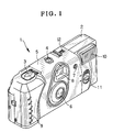
In Fig. 1, a lens-fitted photo film unit 1 has a housing
2 basically formed from plastic material. In an upper face
of the housing 2, there are a shutter release button 3 and a
frame counter window 4, where the number of remaining
available frames is indicated. A packaging belt 5 is wound
on the outside of the housing 2. A taking lens 6 appears in
a front face of the housing 2. There is a photometric window
7, behind which a photometric element is disposed for
detecting reflected flash light from a photographic field.
A viewfinder objective window 8 is disposed higher than the
taking lens 6, and has a viewfinder objective lens. A grip
9 is formed in the housing 2, and includes patterned
projections for preventing slipping. A flash emitter 10 is
incorporated for emitting flash light.
A charger button 11 is slidable up and down, and when
slid up, causes a start of charging the flash device. Upon
completion of the charging, a light-emitting diode (LED) is
driven to illuminate behind a flash standby indicator 12,
where a state ready for flash emission can be checked. Upon
completion of the flash charging, the shutter device is
actuated by depressing the shutter release button 3. The
flash emitter 10 is simultaneously driven to illuminate for
taking an exposure with flash light.
The lens-fitted photo film unit 1, which will be
described later in detail, is provided with a structure for
measuring reflected flash light incident upon the photometric
window 7 at the time of flash photography. If a user intends
photography of an object at a near distance, an amount of
flash light is automatically controlled to prevent an
overexposed state of the principal object with whitish
appearance due to extreme intensity of the reflected flash
light.
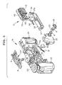
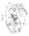
In Fig. 2, the lens-fitted photo film unit 1 includes a
main body 16, a front cover 14 and a rear cover 15. The
front cover 14 and the rear cover 15 cover the front and rear
of the main body 16. A flash device 17 includes a main
circuit board and a main circuit element group mounted on the
main circuit board. A fastening projection 18 is formed to
project from the main body 16, and fastens the flash device
17 on the main body 16 behind the front cover 14. The taking
lens 6 is supported on the center of the main body 16. The
main body 16 includes a shutter device, a shutter charging
mechanism and a one-frame winding mechanism. The shutter
device well-known in the art has a shutter blade 19 disposed
behind the taking lens 6 as depicted in Fig. 3, for
opening/shutting a light path for an exposure upon being
knocked. The shutter charging mechanism operates in response
to rotation of a winder wheel 20, and charges the shutter
device in a manner ready to knock the shutter blade 19. The
one-frame winding mechanism feeds the photo film by one frame
after the shutter device operates, and blocks rotation of the
winder wheel 20.
The main body 16 includes a cassette holder chamber 22
and a photo film chamber 24 formed by molding of the plastic
material. The cassette holder chamber 22 is used to contain
a photo film cassette 21. The photo film chamber 24 is used
to contain a roll of photo film 23 which has been drawn out
of the photo film cassette 21 and externally wound in the
roll form. A cassette spool 25 in the photo film cassette 21
becomes engaged with a core portion of the winder wheel 20.
A portion of the winder wheel 20 appears in an opening
in the rear cover 15. The winder wheel 20, when rotated for
each one exposure, causes the photo film to move toward the
photo film cassette 21 by one frame. In response to rotation
of the winder wheel 20, the shutter device is charged and
becomes ready for next exposure.
An upper combination plate 27 is secured to an upper
wall of the main body 16. The upper combination plate 27 is
constituted by two plate parts, a first of which is opaque
and includes the shutter release button 3, and a second of
which is transparent and colorless and includes the frame
counter window 4.
A photographing opening 30 is formed in a light-shielded
tunnel behind the shutter blade 19. In the rear of the
light-shielded tunnel is formed an exposure aperture for
defining a region of exposure with object light incident
through the photographing opening 30. The photo film is
exposed at the exposure aperture. A return spring 31 has a
first end portion connected with the shutter blade 19, and a
second end portion connected with the main body 16. The
shutter blade 19 is biased by the return spring 31 toward the
closed position to close the photographing opening 30. In
front of the shutter blade 19 are disposed a lens holder 32,
an aperture stop plate 33, the taking lens 6 and a fastening
plate 34.
The flash device 17 includes a main circuit board 17a.
A battery contact segment 37 and the flash emitter 10 are
fixedly secured to the main circuit board 17a. The battery
contact segment 37 supports and contacts a battery 36. A
sync switch 38, a charger power switch 39 and a main
capacitor 40 are mounted on, or directly connected to, the
main circuit board 17a among various circuit elements for the
flash circuit. The sync switch 38 is turned on by opening
operation of the shutter blade 19. The charger power switch
39 is turned on by a shift of the charger button 11. The
main capacitor 40 stores charge at a high voltage.
In the flash emitter 10, a flash discharge tube 41 emits
flash light by discharging the main capacitor 40 that has
stored charge at the high voltage. See Fig. 6. Also, a
reflector is disposed behind the flash discharge tube 41, and
reflects the flash light toward a photographic object with
suitable efficiency.
In Fig. 4 and 5, the flash device 17 includes a
subsidiary circuit board 17b in addition to the main circuit
board 17a. Capacitor terminal pins 40a of the main capacitor
40 are inserted in holes 17c of the subsidiary circuit board
17b, and are fixed and connected with the subsidiary circuit
board 17b by soldering at points 17d. In the fixation of the
capacitor terminal pins 40a, the subsidiary circuit board 17b
is kept oriented perpendicularly to the main circuit board
17a in a rear space. A cutout 42 is formed in the subsidiary
circuit board 17b, and prevents the subsidiary circuit board
17b from contacting circuit elements in the main circuit
board 17a. The main circuit board 17a is equipped also with
an LED (light-emitting diode) 45, an oscillation transistor
46, and an oscillation transformer 47 mounted thereon. The
LED 45 is driven to emit light upon completion of charging
the flash device. The oscillation transistor 46 and the
oscillation transformer 47 are combined as a booster circuit,
and effect oscillation of pulses at a high voltage.
Fig. 6 illustrates the subsidiary circuit board 17b. On
the subsidiary circuit board 17b are mounted a photo
transistor 48 as photometric element, and a flash quenching
circuit or light adjusting circuit 49. As the capacitor
terminal pins 40a of the main capacitor 40 are connected to
the subsidiary circuit board 17b by soldering, the flash
quenching circuit 49 becomes connected electrically in
parallel with the main capacitor 40 and the flash discharge
tube 41 on the side of the main circuit board 17a.
A main circuit element group 50 in the main circuit
board 17a is supplied with power by the battery 36. The
booster circuit or blocking oscillator, which is constituted
by the oscillation transistor 46 and the oscillation
transformer 47, causes the main circuit element group 50 to
charge the main capacitor 40 and a trigger capacitor 51 at a
high voltage of approximately 300 volts. A rectification
diode 52 is connected between the oscillation transformer 47
and each of the main capacitor 40 and the trigger capacitor
51, for preventing a current to flow in reverse to a
predetermined direction of the current of charging.
When the charger button 11 is slid up, the charger power
switch 39 is turned on to start charging. When the changing
is completed, the LED 45 emits light, and can be checked
through the charger button 11. The charger power switch 39
starts operation of the blocking oscillator, and prevents the
discharge of the trigger capacitor 51 at the time except for
the time of turning on of the switch.
After the main capacitor 40 and the trigger capacitor 51
are charged, the use of flash light is enabled if the charger
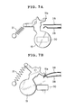
power switch 39 is kept turned on. The shutter release
button 3 is depressed to actuate the shutter blade 19. In
Fig. 7, a blade projection 19a of the shutter blade 19 is
swung together with the shutter blade 19, and contacts and
turn on the sync switch 38. In response to this, the trigger
capacitor 51 is discharged. A trigger transformer 53 in the
trigger circuit is supplied with a current from the trigger
capacitor 51, to generate a breakdown voltage at a high
level. Discharge of the flash discharge tube 41 is
triggered. Then the charge stored in the main capacitor 40
is caused to flow in the flash discharge tube 41, to emit
flash light. As a result, the main circuit element group 50
operates in the flash device for flash light of a
predetermined intensity if without particular additional
circuit elements.
A power supply capacitor 55 is included in the flash
quenching circuit 49, and stores charge for powering circuit
elements in the flash quenching circuit 49. The main circuit
element group 50 also operates to charge the power supply
capacitor 55 at the same time as charging of the main
capacitor 40 and the trigger capacitor 51. There is a Zener
diode 56, in which a current of charging the power supply
capacitor 55 flows.
Upon the discharge in the flash discharge tube 41, a
gate capacitor 57 is charged according to the flow of charge
in the flash discharge tube 41 from the power supply
capacitor 55. There is an SCR (silicon controlled rectifier)
58 as tripolar thyristor having a gate terminal, with which
the gate capacitor 57 is connected. When the power supply
capacitor 55 is discharged, there occurs a potential
difference between the emitter and collector of the photo
transistor 48. Then reflected flash light is detected by the
photo transistor 48, so that a photoelectric current flows
according to a detected amount of the light. An integration
capacitor 59 is charged by the photoelectric current.
When the integration capacitor 59 is charged up to a
predetermined voltage level, then latch transistors 60 and 61
become conductive. Thus, the gate capacitor 57 is
discharged. A current from the same flows through a resistor
62. A gate/trigger voltage, which corresponds to a drop in
the voltage across the resistor 62, is input to the SCR 58,
which is rendered conductive.
When the SCR 58 is rendered conductive, the flow of the
current caused by the discharge of the main capacitor 40 is
changed over from the flash discharge tube 41 to the SCR 58.
At the same time as the change over, the flash emission is
quenched. The remainder of the charge stored in the main
capacitor 40 comes to flow in the SCR 58. A choke coil 64
allows a current from the main capacitor 40 being discharged
to flow at a low frequency to the SCR 58, and protects the
SCR 58 from a current at a high frequency and prevents an
overcurrent from flowing to the SCR 58. An auxiliary
capacitor 65 prevents the latch transistors 60 and 61 from
operating with errors even upon occurrence of electric
noises.
The flash quenching circuit 49 is mounted on the
subsidiary circuit board 17b. The main circuit element group
50 on the main circuit board 17a, therefore, acts as a flash
device with an automatic light adjustment of a bypass type
according to the connection of the flash quenching circuit 49
with the main capacitor 40.
As the various circuit elements are mounted on the main
circuit board 17a and on the subsidiary circuit board 17b in
a separate manner, it is possible selectively to produce
flash devices of an automatic light adjusting type and of a
regular flash emitting type. At first, the main circuit
board 17a with the flash circuit elements but without the
main capacitor 40 is prepared. Also, the subsidiary circuit
board 17b with the flash quenching circuit is prepared. If
the regular flash emitting type of the flash device is
intended in the manufacturing process, the main capacitor 40
can be connected only to the main circuit board 17a. If the
automatic light adjusting type of the flash device is
intended in the manufacturing process, the main capacitor 40
can be connected to the subsidiary circuit board 17b before
being connected to the main circuit board 17a.
Accordingly, it is possible to change the flash device
17 from the automatic adjustable type to the regular flash
emitting type only by attaching and detaching the subsidiary
circuit board 17b with the main capacitor 40. In other
words, a flash device of the regular flash emitting type may
be provided additionally with an automatic adjustable
structure. In conclusion, the construction of the invention
is effective in utilization of common electrical parts
according to general-purpose structures between different
types of products including the automatic adjustable type and
the regular flash emitting type in contrast to the prior
art.
The lens-fitted photo film unit, after being used, is
withdrawn in a collective manner by the manufacturer. The
lens-fitted photo film unit has a form in which the photo
film cassette and photo film have been removed. In a factory
of the manufacturer, the product is checked, repaired and
renewed. After being inspected in a suitable manner, the
product is shipped to the market. This is a recycling
process of the lens-fitted photo film unit. In considering
this situation, the above-described separate structure of the
main circuit board 17a and the subsidiary circuit board 17b
is effective in reducing the number of the steps of
exchanging parts of the product. Lens-fitted photo film
units can be recycled and shipped only at a short period.
Note that the flash device of the invention may be
incorporated in a compact camera. A charger button is
disposed on a camera outer wall to turn on and off a charger
power switch easily. Also, a trigger circuit is energized to
emit flash light at the same time as actuation of the shutter
device.
In Fig. 8, a compact camera 70 of the invention is
illustrated, in which the photo film cassette is loadable and
removable. The compact camera 70 includes a main body 71, a
front cover 72 and a rear cover 73. The front cover 72
includes a lens opening 75, a flash window 77 and a
photometric window 79. A taking lens 74 appears in the lens
opening 75. A flash emitter 76 appears in the flash window
77. A photo transistor 78 as photometric element is disposed
behind the photometric window 79, and measures reflected
flash light. A battery chamber is formed in a side portion
of the main body 71, and is loadable with batteries 80. A
battery chamber lid 81 is disposed on a lower side of the
camera, and openably closes the battery chamber. A cassette
holder chamber 83 is also formed in the main body 71, and is
loaded with a photo film cassette 82. A cassette chamber lid
84 openably closes the cassette holder chamber 83, and keeps
the photo film cassette 82 positioned when locked at the
cassette holder chamber 83. There is a photo film chamber
85, into which the photo film is fed by one frame each time
after an exposure is taken.
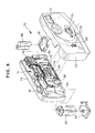
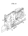
In Fig. 9, a main circuit board 86 and a subsidiary
circuit board 87 are disposed between the main body 71 and
the front cover 72. The main circuit board 86 is not
provided with the flash emitter 10, the battery contact
segment 37 and the sync switch 38 with which the main circuit
board 17a is provided in Fig. 4. However, the other various
elements included in the main circuit board 86 are the same
as those of the main circuit board 17a. A main capacitor 88
is fixedly connected with the main circuit board 86, and
disposed under the taking lens 74. Capacitor terminal pins
88a of the main capacitor 88 are inserted through and
connected with the subsidiary circuit board 87. The
subsidiary circuit board 87 is fastened by soldering to the
capacitor terminal pins 88a, and kept substantially
perpendicular to the main circuit board 86. On the
subsidiary circuit board 87 is mounted the flash quenching
circuit 49 the same as that in the first embodiment.
A plurality of jumper wires are connected with the main
circuit board 86 by soldering. The jumper wires are used to
connect the capacitor terminal pins 88a of the main capacitor
88 to the flash discharge tube in the flash emitter 76, and
to connect some of the flash circuit elements to the
batteries 80 by extending to the battery chamber.
A charger button 90 is disposed in the front cover 72.
A charger power switch 89 is turned on when the charger
button 90 is slid down. The charger button 90 is slidable up
and down in the front cover 72. The charger power switch 89
being turned on, the flash device starts being charged.
After charging, the charger button 90 is kept slid down, to
stand by for an exposure with flash. When a shutter release
button 91 is depressed, a shutter blade is actuated behind
the taking lens 74. The compact camera 70 includes a shutter
device of a knocking type similar to the lens-fitted photo
film unit 1. When the shutter blade opens fully, a pair of
sync switch segments (not shown) contacts each other in the
main body 71, to send a sync signal to the trigger circuit on
the main circuit board 86. The trigger circuit generates
breakdown voltage at a high level, which excites the flash
discharge tube and causes emission of flash light. When
flash light is emitted, the photo transistor 78 measures
reflected flash light. When an integration amount of the
reflected light comes up to a predetermined level, flash
emission is quenched. Thus, the flash light used in taking
an exposure is optimized.
In the above embodiment, the auto flash device controls
the flash light amount automatically. However, it is
possible to mount a photometric circuit on the subsidiary
circuit board 17b, in which a photometric element measures
object brightness, to effect the exposure control by changing
over the stop or exposure amount.
Another preferred embodiment is described with reference
to Figs. 10-18, in which a main capacitor is mounted on a
subsidiary circuit board. In Fig. 10, a front side of a
lens-fitted photo film unit 102 has a taking lens 103, a
viewfinder objective window 104, a charger button 105, a
flash emitter 106 and a photometric window 107. An upper
side of the lens-fitted photo film unit 102 has a shutter
release button 108, a frame counter window 109 and a light
guide 110. The light guide 110 is movable, and when the
charger button 105 is slid up to the charging position, comes
to protrude over the upper side.
In Fig. 11, a winder wheel 120 is disposed on an upper
wall of a cassette holder chamber 116. A photo film cassette
118 has a cassette spool, with which a lower core portion of
the winder wheel 120 is engaged. When the winder wheel 120
is rotated in the counterclockwise direction, an exposed
portion of photo film 119 is wound to the inside of the photo
film cassette 118.
An exposure opening is formed in the front of a light-shielded
tunnel. The shutter blade and a lens holder 121 are
disposed in front of the exposure opening.
A main body 113 has the light-shielded tunnel. A flash
device 124 is fixedly secured to a position between a photo
film chamber 117 and the light-shielded tunnel by use of
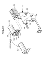
engagement of claws. In Fig. 12, the flash device 124
includes a flash device body 125 and a main capacitor unit
126. The flash device body 125 includes a main circuit board
132, which is provided with the flash emitter 106, a sync
switch 128, a charger power switch 129 and a battery contact
segments 131 all mounted thereon. The charger power switch
129 turns on and off operation of charging the flash device
in sliding of the charger button 105. A battery 130 supplies
power in connection with the battery contact segments 131.
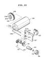
In Fig. 13, the main capacitor unit 126 includes a main
capacitor 134 and a subsidiary circuit board 137, on which
there are mounted a thyristor 135 and a photo transistor 136
as photometric element. A bobbin 139 is secured fixedly to
the main capacitor 134. A choke coil 138 is wound about the
bobbin 139. The photo transistor 136 receives and measures
object light. A photometric element cover 142 covers the
photo transistor 136, and is constituted by a front cover
half 140 and a rear cover half 141. An entrance opening 143
is formed in the front cover half 140. The photo transistor
136 measures reflected flash light entered through the
entrance opening 143. A light reducing filter 144 is
inserted in the entrance opening 143, and consists of an ND
filter for reduction of light. The light reducing filter 144
has a transmittance of a level suitable for a level of a
light amount of the flash light. A light-shielding member
145 is secured to the vicinity of the entrance opening 143 of
the front cover half 140, and prevents the reflected flash
light from entry into the lens-fitted photo film unit 102 as
a leaked light component.
In Fig. 14, there are a flash quenching circuit or light
adjusting circuit 151 and a flash circuit 150 or main circuit
element group included in the flash device 124. The flash
circuit 150 is included in the main circuit board 132. The
flash quenching circuit 151 is included in the subsidiary
circuit board 137. The flash quenching circuit 151 is
connected with the flash circuit 150 by terminal pins of the
main capacitor 134.
An oscillation transformer 155 and an oscillation
transistor 156 constitute a blocking oscillator, and converts
a battery voltage into a high voltage of approximately 300
volts as a booster circuit. The oscillation transformer 155
includes a primary winding 155a, a secondary winding 155b and
a tertiary winding 155c, which are coupled with one another
in mutual induction. A first end portion of the primary
winding 155a is connected with a positive electrode of the
battery 130. A second end portion of the primary winding
155a is connected with a collector of the oscillation
transistor 156. A first end portion of the secondary winding
155b is connected with an anode of a rectification diode 157.
A second end portion of the secondary winding 155b is
connected with a positive electrode of the battery 130
together with a first end portion of the tertiary winding
155c. A second end portion of the tertiary winding 155c is
connected by a resistor 158 to a terminal of the charger
power switch 129.
One terminal of a trigger capacitor 160 in a trigger
circuit is connected via a resistor 159 with a cathode of the
rectification diode 157. Also, a positive terminal of the
main capacitor 134 is connected with the cathode of the
rectification diode 157. A second terminal of the trigger
capacitor 160 is connected with a terminal of the charger
power switch 129. An emitter of the oscillation transistor
156 is connected with a negative electrode of the battery
130. A base of the oscillation transistor 156 is connected
by a resistor 161 with a terminal of the charger power switch
129.
The trigger capacitor 160 is charged by a current output
by the oscillation transformer 155 in a manner similar to the
main capacitor 134. The sync switch 128 is turned on and off
in synchronism with opening/shutting operation of the shutter
blade. A trigger transformer 162 in the trigger circuit
includes a primary winding 162a. When the sync switch 128 is
turned on, the trigger capacitor 160 being charged causes a
current to flow in the primary winding 162a. In response to
this, breakdown voltage occurs in a secondary winding 162b.
A trigger electrode 163 applies the breakdown voltage to a
flash discharge tube 164. Flash light starts being emitted
upon full opening of the shutter blade.
Note that an LED (light-emitting diode) 165 is disposed
under the light guide 110. Electrodes of the LED 165 are
connected with respectively end portions of the tertiary
winding 155c. When the voltage across the main capacitor 134
comes up to a predetermined level for charging, the voltage
across the tertiary winding 155c comes over a predetermined
level, to turn on the LED 165.
The flash quenching circuit 151 on the subsidiary
circuit board 137 is connected in parallel with the flash
discharge tube 164, and in parallel with the main capacitor
134. An operation voltage generator circuit is constituted
by a combination of a capacitor 170, a resistor 171 and a
Zener diode 172. The capacitor 170 is charged by an output
current (300 volts) of the oscillation transformer 155 when
the main capacitor 134 is charged. Charging of the capacitor
170 is stopped when saturation occurs (400 volts, 0.022 µF).
When the main capacitor 134 starts being discharged in a path
with the flash discharge tube 164, the capacitor 170 is also
discharged in a path with the flash discharge tube 164, the
Zener diode 172 and the resistor 171.
The photo transistor 136 has a collector that is
connected by a resistor 174 with a cathode of the Zener diode
172. There are resistors 175 and 176 and a capacitor 177
connected in series between an emitter of the photo
transistor 136 and an anode of the Zener diode 172. The
photo transistor 136 is disposed directly behind the
photometric window 107 formed in a front cover 114 of the
lens-fitted photo film unit 102, and outputs a photoelectric
current according to detected intensity of reflected flash
light from a photographic object. The capacitor 177 is
charged by a photoelectric current from the photo transistor
136 at a voltage level which increases gradually. In other
words, light intensity of the reflected flash light received
by the photo transistor 136 is converted to voltage. A photo
diode or other illuminating device may be used instead of the
photo transistor 136.
A switching unit 180 includes transistors 181 and 182.
A base of the transistor 181 is connected with a connection
point between the resistors 175 and 176. Also, a collector
of the transistor 182 is connected with the same connection
point. A collector of the transistor 181 is connected with
a base of the transistor 182. An emitter of the transistor
181 is connected with an anode of the Zener diode 172. An
emitter of the transistor 182 is connected by the resistor
174 with a cathode of the Zener diode 172. When the voltage
across the capacitor 177 comes up to a predetermined level,
the transistors 181 and 182 in the switching unit 180 are
turned on. The turning on of the switching unit 180
generates a quench signal for quenching emission of flash.
A capacitor 184 and a resistor 185 constitute an onvoltage
generating circuit. One terminal of the capacitor
184 is connected with an anode of the Zener diode 172. One
end portion of the resistor 185 is connected with a cathode
of the Zener diode 172. The capacitor 184 is charged via the
resistor 185 by a voltage generated across the Zener diode
172. When the switching unit 180 is turned on, the capacitor
184 is discharged in a path with the resistor 185, the
resistor 174 and the switching unit 180. A gate voltage
occurs across the resistor 185 for rendering the thyristor
135 conductive.
A gate and cathode of the thyristor 135 are connected to
respectively end portions of the resistor 185. An anode and
the cathode of the thyristor 135 are connected to
respectively terminals of the main capacitor 134. Thus, the
voltage across the main capacitor 134 being charged is
applied between the anode and cathode of the thyristor 135.
Voltage across the resistor 185, which occurs upon
discharging the capacitor 184, is applied between the gate
and cathode of the thyristor 135.
The operation of the above construction is described.
In Fig. 13, the subsidiary circuit board 137 having the flash
quenching circuit 151 is prepared, to which the thyristor 135
and the photo transistor 136 are attached by soldering. A
hole 139a is formed in the bobbin 139, into which capacitor
terminal pins 134a and 134b of the main capacitor 134 are
inserted. The capacitor terminal pins 134a and 134b are
inserted in cutouts 137a and 137b formed in the subsidiary
circuit board 137, for attachment by soldering. Subsidiary
board terminals 151a and 151b of the flash quenching circuit
151 are located in the vicinity of the cutouts 137a and 137b
of the subsidiary circuit board 137. The capacitor terminal
pins 134a and 134b are attached to the subsidiary board
terminals 151a and 151b by soldering so as to connect the
main capacitor 134 electrically with the flash quenching
circuit 151. A projection 139b is formed to project from the
bobbin 139, and positions the main capacitor 134 exactly
relative to the subsidiary circuit board 137. A first end
portion of the choke coil 138 is attached by soldering to the
capacitor terminal pin 134a of the main capacitor 134. A
second end portion of the choke coil 138 is attached by
soldering to a contact point of the subsidiary circuit board
137. The choke coil 138 is in series with an anode of the
thyristor 135. As a result, the main capacitor unit 126 is
obtained.
In Fig. 12, the main capacitor unit 126 is secured to a
predetermined position of the main circuit board 132 where
the flash emitter 106, the sync switch 128 and the battery
contact segments 131 are mounted. The subsidiary circuit
board 137 is approximately perpendicular to the main circuit
board 132. The capacitor terminal pins 134a and 134b of the
main capacitor 134 are attached by soldering to electrodes of
the flash discharge tube 164 for parallel connection, in a
suitable position of the flash circuit 150 on the main
circuit board 132. So the flash quenching circuit 151 is
connected with the flash circuit 150. Then an amount of
reflected flash light is experimentally measured. The light
reducing filter 144 of a type with transmittance according to
the measured light amount is inserted in the entrance opening
143 of the front cover half 140. Now the flash device 124 is
constructed as a product. The flash device 124 being
obtained finally is secured to the main body 113 of the
lens-fitted photo film unit 102, to which the front cover 114
is attached. Then the photo film cassette 118 and a photo
film roll 119a being unexposed are inserted in respectively
the cassette holder chamber 116 and the photo film chamber
117. A rear cover 115 is secured suitably.
In Fig. 12, the exchange of the main capacitor is
illustrated. To construct a flash device without an
automatic light adjustment, an alternative main capacitor 187
is attached instead of the main capacitor unit 126. Terminal
pins of the main capacitor 187 are attached to contact points
the same as those to which the capacitor terminal pins 134a
and 134b of the main capacitor 134 are attached. The use of
the main capacitor 187 makes it possible to construct the
conventional type of flash device. The flash device body 125
is compatible for the two types, one with the main capacitor
unit 126 and another with the main capacitor 187.
Still another preferred embodiment is described, in
which subsidiary board terminal patterns 190a and 190b are
utilized for connecting the flash quenching circuit with the
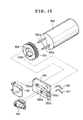
flash circuit. In Fig. 15, a subsidiary circuit board 190
has two surfaces on which a flash quenching circuit or light
adjusting circuit is formed. A thyristor 191 and a light
measuring device 192 with a photometric element are attached
to the subsidiary circuit board 190 by soldering. A choke
coil 193 is wound about a bobbin 194, which is secured to a
main capacitor 195. Capacitor terminal pins 195a and 195b
protrude from the main capacitor 195, and are attached to
respectively the subsidiary board terminal patterns 190a and
190b of the subsidiary circuit board 190. There are
connection terminals 196 and 197 which are connected with the
subsidiary board terminal patterns 190a and 190b at contact
points 190c and 190d. As the connection terminals 196 and
197 are disposed in the flash device body, it is possible to
provide automatic light adjustment in the flash device.
Another preferred embodiment is described, in which a
structure for controlling stop of a photographic light path
is added. In Fig. 16, a main circuit board includes a flash
circuit 201 or main circuit element group, and an exposure
control circuit 202. On the main circuit board are mounted
a CdS photoreceptor element 203 and a solenoid 204. The CdS
photoreceptor element 203 measures a light amount of ambient
light. The solenoid 204 is driven to change over the
aperture stop. A flash quenching circuit or light adjusting
circuit 206 is included in a subsidiary circuit board, on
which a thyristor 207 and a photo transistor 208 as
photometric element are mounted. A choke coil 209 is
associated with a main capacitor 210. The subsidiary circuit
board is attached to the main capacitor 210 to construct a
main capacitor unit 215. The choke coil 209 has a first end
portion 209a, with which a negative terminal pin 210a of the
main capacitor 210 is connected. Note that a battery 211
supplies power. A flash discharge tube 212 emits flash to
illuminate a photographic field.
In Fig. 17, assembly of the main capacitor unit 215 is
depicted. A subsidiary circuit board 217 is oriented
substantially perpendicular to a main circuit board 216. The
negative terminal pin 210a and a positive terminal pin 210b
of the main capacitor 210 are attached to contact points of
the flash circuit 201. Also, an input terminal 218 of the
subsidiary circuit board 217 is attached by soldering to an
output terminal 219 of a line from the exposure control
circuit 202 in the main circuit board 216. Therefore, the
flash quenching circuit 206 is connected with the exposure
control circuit 202. An ambient light state signal can be
output to the flash quenching circuit 206. As the main
circuit board 216 is soldered to the subsidiary circuit board
217, the fastening structure can be firm. A second end
portion 209b of the choke coil 209 is attached by soldering
to a metal contact segment 241 connected with one electrode
of the flash discharge tube 212. Thus, it is possible to
provide automatic light adjustment in the flash device.
Furthermore, a projection 242 may be formed on the subsidiary
circuit board 217. An opening 243 may be formed in the main
circuit board 216, and receive insertion of the projection
242. Contact points at the projection 242 can be attached to
contact points near to the opening 243 by soldering. As the
main circuit board 216 is soldered to the subsidiary circuit
board 217 in the two positions, the fastening structure is
remarkably firm.
In Fig. 18, a compact camera of the invention is
illustrated. A camera 220 includes a main body 221, and a
front cover 222 and a rear cover 223 for covering the front
and rear of the main body 221. The main body 221 includes a
shutter mechanism, photo film advancing mechanism and the
like for taking an exposure. A flash device 224 is disposed
between the main body 221 and the front cover 222. Unlike
the flash device 124 according to Fig. 11, the flash device
224 does not have the battery contact segments 131. However,
remaining portions of the flash device 224 are the same as
those of the flash device 124. Note that the flash device
224 of the invention is provided with the main capacitor unit
126 according to the above embodiments. A cassette chamber
lid 226 is disposed on a lower face of the camera 220 for
inserting a photo film cassette 225. Batteries 227 supply
power. A battery chamber lid 228 is opened and closed for
loading of the batteries 227.
A charger button 231 is disposed in the front cover 222.
A charger power switch 230 of the flash device 224 is turned
on upon pushing of the charger button 231. When flash light
is emitted and directed back by reflection, a light measuring
device 232 with a photometric element measures the reflected
flash light. When an integration amount of the reflected
light comes up to a predetermined level, flash emission is
quenched. Thus, the flash light applied in taking an
exposure is optimized.
A further preferred embodiment is described with
reference to Figs. 19-26, in which a discharge tube case is
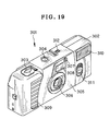
used. In Fig. 19, a lens-fitted photo film unit 301 has a
housing 302 basically formed from plastic material. In an
upper face of the housing 302, there are a shutter release
button 303 and a frame counter window 304, where the number
of remaining available frames is indicated. A packaging belt
305 is wound on the outside of the housing 302. A taking
lens 306 appears in a front face of the housing 302. There
is a photometric window 307, behind which a photometric
element is disposed for detecting reflected flash light from
a photographic field. A viewfinder objective window 308 is
disposed higher than the taking lens 306, and has a
viewfinder objective lens. A grip 309 is formed in the
housing 302, and includes patterned projections for
preventing slipping. A flash emitter 310 is incorporated for
emitting flash light.
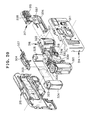
In Fig. 20, the lens-fitted photo film unit 301 includes
a main body 316, a front cover 314 and a rear cover 315. The
front cover 314 and the rear cover 315 cover the front and
rear of the main body 316. A flash device 317 includes a
main circuit board and a main circuit element group mounted
on the main circuit board. A fastening projection 318 is
formed to project from the main body 316, and fastens the
flash device 317 on the main body 316 behind the front cover
314.
The main body 316 includes a cassette holder chamber 321
and a photo film chamber 322 both formed by molding of the
plastic material. The cassette holder chamber 321 is used to
contain a photo film cassette 324. The photo film chamber
322 is used to contain a roll of photo film 325 which has
been drawn out of the photo film cassette 324 and externally
wound in the roll form. A cassette spool 323 in the photo
film cassette 324 becomes engaged with a core portion of the
winder wheel 320.
An upper combination plate 327 is secured to an upper
wall of the main body 316.
In front of the shutter blade are disposed a lens holder
330, an aperture stop plate, the taking lens 306 and a
fastening plate 332.
The flash device 317 includes a main circuit board 317a.
A battery contact segment 335 and the flash emitter 310 are
fixedly secured to the main circuit board 317a. The battery
contact segment 335 supports and contacts a battery 334. A
sync switch 336, a charger power switch 337 and a main
capacitor 338 are directly connected with the main circuit
board 317a among various circuit elements for the flash
circuit. The sync switch 336 is turned on by opening
operation of the shutter blade. The charger power switch 337
is turned on by a shift of the charger button 311. The main
capacitor 338 stores charge at a high voltage.
In Fig. 21, the flash emitter 310 includes a flash
discharge tube 339 and a discharge tube case 340. The flash
discharge tube 339 is supplied with power by the main
capacitor 338 charged at a high voltage, and emits flash
light. The discharge tube case 340 contains the flash
discharge tube 339. A projection 340a is formed to project
from an end of the discharge tube case 340. A retention hole
342 is formed in the main circuit board 317a, retains the
projection 340a to fasten the discharge tube case 340 to the
main circuit board 317a.
The main capacitor 338 has a pair of capacitor terminal
pins 338a, which are attached by soldering to a subsidiary
circuit board 317b. However, a support plate 341 is disposed
between the subsidiary circuit board 317b and the main
capacitor 338. Also, a photo transistor 343 as a photometric
element is mounted on the subsidiary circuit board 317b for
measuring reflected flash light. A light reducing filter 344
is disposed in front of the photo transistor 343. A
photometric element cover 345 is disposed about the photo
transistor 343. A cushioning tube 346 made of sponge,
polyurethane foam or other porous material is fitted on the
outside of the photometric element cover 345. It follows
that a main capacitor unit 348 is constructed by the
subsidiary circuit board 317b and the main capacitor 338
mounted on the subsidiary circuit board 317b.
Grooves 341a are formed in the support plate 341,
receive insertion of the capacitor terminal pins 338a that
are bent rectangularly at two points. The main capacitor 338
is precisely positioned on the support plate 341 by the
insertion into the support plate 341. In Fig. 22, two
retention hooks 341b are formed to project from the support
plate 341, engaged with the inside of cutouts 347 in the
subsidiary circuit board 317b, to retain the subsidiary
circuit board 317b firmly. A plate engaging ridge 340b is
formed to project from the projection 340a, and secures the
support plate 341 to the discharge tube case 340 to position
the subsidiary circuit board 317b.
An engagement hole 340c is formed in the plate engaging
ridge 340b. An engagement rod 341c projects from the support
plate 341, is fitted in the engagement hole 340c to position
the support plate 341. Engagement hooks 341d are formed to
project from the support plate 341 in upper and lower
positions, and engaged with the plate engaging ridge 340b for
retention with the engagement rod 341c. Thus, the support
plate 341 is fastened to the discharge tube case 340. In
Fig. 23, the support plate 341 keeps the subsidiary circuit
board 317b fixed substantially perpendicularly with reference
to the main circuit board 317a.
In Fig. 24, the photometric element cover 345 covers the
photo transistor 343. Press ridges 350 are formed inside the
photometric element cover 345, and tightly hold the light
reducing filter 344 that is thrust between the press ridges
350. An entrance opening 351 is formed in front of the
photometric element cover 345, and is opposed to the
photometric window 307. The cushioning tube 346 operates at
the time of flash emission, and prevents flash light from
entry in the entrance opening 351 even though light leaks
from the discharge tube case 340 to the inside of the front
cover 314. Thus, the photo transistor 343 detects light only
from the photographic field. The light reducing filter 344
is formed from transparent plastic material having a
prescribed optical transmittance, and reduces intensity of
incident light from the entrance opening 351, to adjust photo
sensitivity of the light measuring device with the photo
transistor 343. The light reducing filter 344 has optical
transmittance that is suitable according to sensitivity of
the photo transistor 343. Note that, if the sensitivity of
the photo transistor 343 is remarkably high, it is possible
to use two or more light reducing filters 344 in the
photometric element cover 345 to reduce the intensity of
transmitted light.
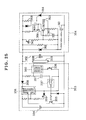
In Fig. 25, a main circuit element group 353 is mounted
on the main circuit board 317a. A flash quenching circuit or
light adjusting circuit 354 is included in the subsidiary
circuit board 317b. The capacitor terminal pins 338a are
attached to the subsidiary circuit board 317b by soldering,
to connect the flash quenching circuit 354 with the main
capacitor 338 electrically. In Fig. 24, a lead wire 352
connects the capacitor terminal pins 338a with the main
circuit element group 353. The flash quenching circuit 354
is connected in parallel with the main circuit element group
353 with reference to the main capacitor 338.
The main circuit element group 353 in the main circuit
board 317a is supplied with power by the battery 334. The
booster circuit or blocking oscillator, which is constituted
by an oscillation transistor 355 and an oscillation
transformer 356, causes the main circuit element group 353 to
charge the main capacitor 338 and a trigger capacitor 357 at
a high voltage of approximately 300 volts. A rectification
diode 358 is connected between the oscillation transformer
356 and each of the main capacitor 338 and the trigger
capacitor 357, for preventing a current from flowing in
reverse to a predetermined direction of the current of
charging.
A charger button 311 is slid to turn on the charger
power switch 337. Then the blocking oscillator is energized
to start charging. A light-emitting diode (LED) 359 is
driven at the time shortly before the end of the charging
operation. A flash standby indicator 312, which transmits
light from the LED 359, enables an user to check the
completion of the charging with the LED 359.
When the trigger capacitor 357 is discharged, a trigger
transformer 360 in the trigger circuit is supplied with a
current from the trigger capacitor 357, to generate a
breakdown voltage at a high level to trigger the flash
discharge tube 339.
A power supply capacitor 361 is included in the flash
quenching circuit 354, and stores charge for powering circuit
elements in the flash quenching circuit 354. The main
circuit element group 353 also operates to charge the power
supply capacitor 361 at the same time as charging of the main
capacitor 338 and the trigger capacitor 357. There is a
Zener diode 362, in which a current of charging the power
supply capacitor 361 flows.
Upon application of the breakdown voltage to the flash
discharge tube 339, a gate capacitor 363 is also charged
according to the flow of a current from the power supply
capacitor 361. There is an SCR (silicon controlled
rectifier) 364 as tripolar thyristor having a gate terminal,
with which the gate capacitor 363 is connected. When the
power supply capacitor 361 is discharged, there occurs a
potential difference between the emitter and collector of the
photo transistor 343. Then reflected flash light is detected
by the photo transistor 343, so that a photoelectric current
flows according to a detected amount of the light. An
integration capacitor 365 is charged by the photoelectric
current.
When the integration capacitor 365 is charged up to a
predetermined voltage level, then latch transistors 366 and
367 become conductive. Thus, the gate capacitor 363 is
discharged. A current from the same flows through a resistor
368. In response to this, a potential difference occurs
between a gate and cathode of the SCR 364 at a level that
corresponds to a drop in the voltage across the resistor 368,
so the SCR 364 is rendered conductive.
When the SCR 364 is rendered conductive, flow of the
current caused by the discharge of the main capacitor 338 is
changed over from the flash discharge tube 339 to the SCR 364
having smaller resistance. At the same time as the change
over, the flash emission is quenched. The remainder of the
charge stored in the main capacitor 338 causes a current to
flow in the SCR 364. It is to be noted that an auxiliary
capacitor 369 prevents the latch transistors 366 and 367 from
operating with errors even upon occurrence of electric
noises.
In Fig. 26, a compact camera 370 of the invention is
illustrated, in which the photo film cassette is loadable and
removable. The compact camera 370 includes a main body 371,
a front cover 372 and a rear cover 373. The front cover 372
includes a lens opening 375, a flash window 377 and a
photometric window 379. A taking lens 374 appears in the
lens opening 375. A flash emitter 376 appears in the flash
window 377. A light measuring device 378 with a photometric
element is disposed behind the photometric window 379, and
measures reflected flash light. A battery chamber is formed
in a side portion of the main body 371, and is loadable with
batteries 380. A battery chamber lid 381 is disposed on a
lower side of the camera, and openably closes the battery
chamber. A cassette holder chamber 383 is also formed in the
main body 371, and is loaded with a photo film cassette 382.
A cassette chamber lid 384 openably closes the cassette
holder chamber 383, and keeps the photo film cassette 382
positioned when locked at the cassette holder chamber 383.
There is a photo film chamber 385, into which the photo film
is fed by one frame each time after an exposure is taken.
A main circuit board 386 is not provided with the flash
emitter 310, the battery contact segment 335, and the sync
switch 336 of the main circuit board 317a of Fig. 21.
However, a main capacitor 388 is mounted on or directly
connected with the main circuit board 386. Other various
circuit elements of the main circuit board 386 are the same
as those of the main circuit board 317a. A subsidiary
circuit board 387 is secured to a lateral wall of the flash
emitter 310 by screws and screw holes.
A charger button 390 is disposed in the front cover 372.
A charger power switch 389 inside the charger button 390 is
turned on by shifting the charger button 390. When a shutter
release button 391 is depressed, a shutter blade is actuated
behind the taking lens 374.
It is to be noted that, although the main capacitor 388
is disposed under the taking lens 374 according to Fig. 26,
a camera of the invention may have the main capacitor 388
disposed behind the flash emitter 376 and beside the
subsidiary circuit board 387. In other words, the subsidiary
circuit board 387 in the camera may be combined with the main
capacitor 388 in a directly connected state to constitute a
main capacitor unit.
Furthermore, the subsidiary circuit board 317b, the
subsidiary circuit board 387 may be fixedly secured to the
discharge tube case 340 by means of adhesive agent in
addition to engagement of claws or screws.
Although the present invention has been fully described
by way of the preferred embodiments thereof with reference to
the accompanying drawings, various changes and modifications
will be apparent to those having skill in this field.
Therefore, unless otherwise these changes and modifications
depart from the scope of the present invention, they should
be construed as included therein.