The present invention relates, in general, to an electrical circuit and method for
mitigating the effects of a current increase due to a fault within the circuit. The
invention is particularly, but not exclusively, concerned with a current increase
across a laser diode due to an electrical short within the circuit.
In the field of integrated circuits, it is known that faults may occur in the
structure of an integrated circuit. These structural faults may occur during the
manufacturing process or alternatively they may arise during use either as a
result of material weaknesses or misuse of the circuit. It is very difficult to locate
all faults in an integrated circuit prior to use. Unfortunately, undetected faults
may cause the integrated circuit (and any electrical devices that it is coupled to)
to fail in their operation.
It is known in the art to design electrical circuits which are 'fault tolerant'. A fault
tolerant circuit is generally configured so that a failure of strategic components
does not result in the complete loss of circuit operation.
Where an integrated circuit includes a laser diode within the circuitry,
undetected faults may be especially problematic. For example, if the integrated
circuit were shorted to ground as a result of a component of the integrated
circuit failing, then a significant increase in current across the laser diode may
occur. The current increase may cause light intensity emitted from the laser
diode to increase because the light intensity output from the laser diode is
proportional to the current drawn. An increase in light intensity output may
represent significant danger to a user of the laser diode circuit, the danger
arising from inadvertent projection of the laser light into the user's eye. In this
regard, all laser circuits must be stringently tested for compliance with stipulated
regulatory requirements, which testing is arduous and therefore expensive. In
any event, even if a circuit passes the regulating (safety) tests, there is no
guarantee that a fault will not emerge with time with a particular device, which
fault could generate a localised current that drives the laser divide output
beyond stipulated light intensity outputs and into an unsafe operational state.
There is therefore a need to produce an electrical circuit which mitigates the
problem of an increase in current resulting from an undetected or unexpected
electrical fault.
According to a first aspect of the present invention, there is provided an
electrical circuit containing a first circuit having associated therewith a first
track supporting, in use, a first current; and a second circuit drawing, in
use, a second current, the second circuit located proximate to the first
track, the electrical circuit characterised by an electrical shield providing an
electrically isolated enclosure, the electrical shield positioned substantially
about the first track and such that the shield inhibits, in use, shorting of the
first track to the second circuit to restrict, in use, substantial summing of
the first current with the second current.
The shield, in use and under fault conditions, may inhibit establishment of a
short circuit supporting flow of a current greater than a predetermined
threshold through an electrical component.
The electrical component may be a laser diode, and the second circuit may
be a track. Also, the shield may comprise at least one metal layer within an
integrated circuit or printed circuit board, the shield further including at
least one via.
In a second aspect of the present invention there is provided an electrical
device comprising the electrical circuit of the first aspect of the present
invention.
In a third aspect of the present invention there is provided an integrated circuit
or printed circuit board comprising the electrical circuit of the first aspect of the
present invention or the electrical device of the second aspect of the present
invention.
In a fourth aspect of the present invention there is provided a method of
mitigating effects of a short circuit fault condition within an electrical
circuit, the method comprising determining a current sensitive circuit; and
providing a ground insulated shield substantially about said current sensitive
circuit to prevent, in use, a short circuit fault condition associated with a
second electrical circuit from increasing current through the current
sensitive circuit.
The invention may also comprise a method of laying out the electrical circuit
such that at least one metal layer and at least one via of the non-critical track
form a shield around a greater part of the determined critical track.
Advantageously, a fault tolerant integrated circuit may be achieved by the layout
of the circuit components and, where the circuit includes a laser diode, a
sudden increase in light intensity output by the laser diode (which may damage
the eyes of the user) may be avoided. Specifically, a track including the laser
diode is identified and insulated by means of a layout of the circuit ( metal layers
and vias are utilised to form an insulating shield around the laser diode).
The present invention is generally applicable to electrical circuits which require
protection from current overload and, whilst being particularly applicable to
integrated circuits which include at least one laser diode, can be employed
more widely.
An embodiment of the present invention will now be described by way of
example only and with reference to the accompanying drawings, in which:
FIG. 1 illustrates a vertical cross-sectional view through a known integrated
circuit 10. Metal layer 12 and metal layer 14 (each metal layer including at least
one track, i.e. a conducting path) are separated by a first layer of insulation (e.g.
oxide) 18 within an integrated circuit of the like. Metal layer 14 and metal layer
16 are separated by a second insulation layer 20. In this three-metal system,
metal layer 12 is electrical ground. A via (which is an electrical connection
between layers of metal) 22, 24 connects layers 12 and 14, and layers 14 and
16 respectively. A track on metal layer 14 is connected to a laser diode (not
illustrated) that is typically external to an integrated circuit (IC).
In operation, a fault within the integrated circuit 10 may result in an unwanted
electrical bridging between two of the metal layers 12, 14, 16 as the circuit
shorts to ground. For example, if a fault occurred within metal layer 14, this may
result in a significant increase in current across components (including the laser
diode) in the track in metal layer 14. The resulting increased light intensity may
be damaging to a user's eyes or have other unwanted detrimental effects
depending on the use of the integrated circuit.
FIG. 2 illustrates a front view of a vertical cross-section through an integrated
circuit 40 incorporating the concepts of the present invention. Metal layer 42 is
grounded and metal layer 44 supports separate tracks 44a, 44b and 44c. The
track contained in metal layer 44b is identified as being strategically significant
to the functioning of the integrated circuit 40, since track 44b draws an amount
of current that could combine with secondary current in another independent
circuit in a short circuit environment, to present an increased current source to
and through a laser diode. A metal layer 46 and the metal layer 42 are
connected to tracks 44a and 44c with vias 50. Thus, a metal shield is created
around the strategically current-significant track 44b, thereby electrically
insulating or isolating the current from shorting through the laser diode.
In operation, a fault within the integrated circuit 40 may result in an unwanted
electrical bridging between two of the metal layers 42, 44, 46 as the circuit
shorts to ground. However, the operationally sensitive track 44b will not be
affected by the short because it is effectively insulated by the metal shield
created by the layout of the integrated circuit.
FIG. 3 illustrates a vertical cross-sectional view of an integrated circuit of an
alternative embodiment of the present invention. Metal layer 62 is grounded and
metal layer 64 contains separate tracks 64a, 64b and 64c. The track contained
in metal layer 64b is identified as being strategically significant to the functioning
of the integrated circuit 60, since track 64b draws an amount of current that
could combine with secondary current in another independent circuit in a short
circuit environment, to present an increased current source to and through a
laser diode. A plurality of vias 68 extend from tracks 64a and 64c. One of said
vias 68 is connected between track 64a and the metal layer 62 and another one
of said vias 68 is connected between track 64c and the metal layer 62. Thus, a
metal shield is created around the strategically current-significant track 64b,
thereby electrically insulating or isolating the current from shorting through the
laser diode.
Thus, the sensitive track 64b is insulated on three sides by a grounded metal
shield, leaving the upper side uninsulated. In operation, bridging to the track
64b is avoided as it is only necessary to have insulation between tracks of a
single layer but not at both the upper and lower sides. Therefore, a further
embodiment of the present invention comprises the sensitive track insulated on
three sides by a grounded metal shield, leaving the lower side uninsulated.
FIG. 4 illustrates a side view of a vertical cross-sectional view through a multilayer
integrated circuit 70 incorporating the concepts of the present invention. A
first circuit 72, in use, generally draws relatively high levels of current, but at
least significant amounts of current that warrant concern in relation to laser light
intensity output if the first circuit electrically shorts, i.e. combines with a second
circuit 74. One of the first or second circuits will have a conduction path to a
laser diode that affects, i.e. provides, operating current to the laser diode. An
electrically insulated shield 76 realised by metal tracks or layers 44a and 44c
therefore isolates the first circuit 72 from the second circuit under fault or multi-fault
conditions to ensure that current through the laser diode never exceeds
predetermined safety levels. In other words, the shield 76 protects against a
short between "Signal A" and "Signal B". The shield 76 may include vias (not
shown for the sake of clarity). Operation of a circuit including this component
layout is described above with reference to FIG. 2. The shield 76 is tied to a
safe (i.e. stable) potential, typically selected to be ground potential.
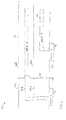
FIG. 5 illustrates a plan view of an integrated circuit (IC) 80 incorporating a track
42a insulated according to a preferred embodiment of the present invention.
Bond pads 92 are typically spaced along a periphery of the IC 80. To exemplify
the requirements for an deployment of the present invention, it is useful to
consider the circuit scenario where a bond pad 93 in the top left-hand corner of
the IC 80 is connected to first circuit 72 via insulated track 44b. The track 44b is
insulated by a shield 76 (as illustrated in FIG. 2 or FIG. 3) as the track 44b and
traverses a second circuit 74. The second circuit 74 receives drive current from
a current supply 88 which, in turn, is coupled to the first circuit 72. A laser diode
90 is coupled between the first circuit 72 and the second circuit 74 using bond
pads to provide an off-chip connection. Clearly, the IC 80 also includes further
tracks that connect bond pads to the components mounted on the IC 80.
In operation, bridging between the second circuit 74 and the sensitive track 44b
is avoided due to the insulating shield 76. Therefore, if a fault occurs between
the first circuit 72 and the second circuit 74, the shield 76 acts to prevent any
significant (and preferably any absolute) increase in light intensity output by the
laser diode 90 (as a consequence of increased current through the laser diode
arising by virtue of a short-circuit. The shield 76 preferably entirely encloses the
track 44b, although the degree of encapsulation is a design feature dictated by
the sensitivity of the track 44b in terms of its current shorting capabilities. In
other words, the shield 76 may be sufficient if it substantially but not totally
encapsulates the track 44b, with the shield acting to provide the requisite
electrical isolation by virtue of its physical location and presence.
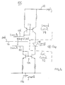
Looking briefly at FIG. 6, the present invention is shown implemented within
a typical circuit 100. For the sake of explanation, the first circuit is coupled
to trace A (reference numeral 102), the trace providing current to a first
current mirror circuit 104 coupled to ground 106 via resistive networks.
The second circuit 74 is coupled to trace B (reference numeral 108), the
trace connected to a second current mirror 110 coupled to a power supply
112 through an appropriate resistive network. The first circuit 72 and the
second circuit are coupled together through laser diode 90. In absence of
the shield 76 of the present invention, any short between trace A and trace
B could result in a near infinite amount of current flowing through the laser
diode 90.
In summary, according to an underlying inventive concept, a system of a
preferred embodiment functions to mitigate the effects of a current increase due
to a fault within an integrated circuit.
It will be appreciated that the above description has been given by way of
example only and that modifications in detail may be made within the scope of
the invention. For example, whilst the present invention has been generally
described in relation to a three-metal system of an integrated circuit, the
underlying concept can be employed in integrated circuits comprising a different
number of metal layers (e.g. a six-layer design). Also, the integrated circuit of
the present invention may have a layout wherein any part of the metal shield is
connected to ground. Furthermore, while the present invention has particular
applicability to laser diode circuits, it will be appreciated that the inventive
concept of shielding one track from another to avoid an excess current condition
in a circuit is more generally applicable (even to the extent that the shielding
prevents damage and protects a costly (expensive) discrete device or the like).
Indeed, the present invention can find application in printed circuit boards
(PCBs).