EP1255255A2 - High speed decoder for flash memory - Google Patents
High speed decoder for flash memory Download PDFInfo
- Publication number
- EP1255255A2 EP1255255A2 EP02251716A EP02251716A EP1255255A2 EP 1255255 A2 EP1255255 A2 EP 1255255A2 EP 02251716 A EP02251716 A EP 02251716A EP 02251716 A EP02251716 A EP 02251716A EP 1255255 A2 EP1255255 A2 EP 1255255A2
- Authority
- EP
- European Patent Office
- Prior art keywords
- word line
- gate
- source
- transistors
- transistor
- Prior art date
- Legal status (The legal status is an assumption and is not a legal conclusion. Google has not performed a legal analysis and makes no representation as to the accuracy of the status listed.)
- Granted
Links
Images


Classifications
-
- G—PHYSICS
- G11—INFORMATION STORAGE
- G11C—STATIC STORES
- G11C16/00—Erasable programmable read-only memories
- G11C16/02—Erasable programmable read-only memories electrically programmable
- G11C16/06—Auxiliary circuits, e.g. for writing into memory
- G11C16/08—Address circuits; Decoders; Word-line control circuits
Definitions
- This invention relates to decoders for flash memories, and more particularly to a fast xdecoder using NMOS driver circuitry in combination with a time delay scheme to insure efficient boost operation.
- Flash memories conventionally consist of an array of floating gate transistors or core cells that are arranged in blocks and are individually addressable by energizing a specific word line and a specific bit line of the array.
- a "0" on a core cell corresponds to a high turn-on threshold voltage on the order of 4V for the cell, while a “1” corresponds to a low turn-on threshold voltage on the order of 2V.
- the word line for each cell is connected to its transistor's control gate, and the bit line for its address powers its source-drain circuit.
- a cell is read by driving its word line to a voltage between the above-mentioned threshold voltages while its source-drain circuit is energized. If current flows, the cell contains a "1"; if not, it contains a "0.”
- V CC voltage boosting circuit
- V BST boost voltage
- Such a circuit is quite sensitive to parasitic capacitance loading. It is in the nature of a CMOS driver for an xdecoder that is global word line must be low in order for the cell to be selected. Consequently, the word lines of all unselected cells must be high, a condition which loads the boost circuit and slows it down. Thus, for fast operation, it is desirable to provide a way of increasing boosting without loading the boost circuit.
- the present invention can solve some or all of the above-described problems by providing word line drivers using NMOS transistors, in combination with a time-delay addressing scheme that uses the driver transistors' gate capacitance to provide an extra boost.
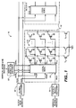
- Fig. 1 illustrates a typical flash memory 10.
- the memory 10 is conventionally arranged in blocks 12 containing, for example, an array of 8x8 core cells or floating gate transistors 14.
- Each block 12 includes a local xdecoder 16 whose inputs are a positive global word line PGW, a negative global word line NGW, and (in Fig. 1) eight vertical word lines AVW 0 through AVW 7 .
- the outputs of the local xdecoder 16 are the word lines WL 0 through WL 7 , each of which serves as the word line for one horizontal row of core cells 14 in the block 12.
- Individual core cells 14 of a given horizontal row are addressed by turning on a selected one of bit line transistors Y 0 through Y 7 .
- Fig. 2 shows the details of the local xdecoder 16 according to the invention.
- the 8x8 block of Fig. 1 there are eight drivers 20 0 through 20 7 that produce the word line signals WL 0 through WL 7 .
- Each of the drivers consists of a series-connected pair of n-transistors 22, 24 and a word line gate n-transistor 26.
- the control gate of transistor 26 is connected to a word line gate signal WLG whose generation is described below in connection with Fig. 5.
- the boost voltage generator 30 may consist of an inverter 32 in series at node 38 with a boost capacitor 34 and in parallel with the gate-source circuit of an n-channel transistor 36.
- V K A normally high kickback voltage V K is applied to the input of inverter 32 so that the V BST output of capacitor 34 is connected to V CC through transistor 36.
- V K goes low, node 38 goes high to V CC , and with transistor 36 now cut off, V BST goes to V CC plus the voltage stored on capacitor 34.
- V K returns to high and readies the circuit for the next read operation.
- pull-up transistors 22 and 24 are n-channel transistors
- the nodes 28 which are the gates of transistors 22 must be kept high enough to turn them on.
- a self-boosting scheme is used. For this purpose, AVWL and WL are kept low until the node 28 reaches a high enough voltage during the rise of PGW and WLG to the level of V BST . Then, when AVWL is allowed to rise to V BST , the voltage at node 28 is automatically boosted above V BST due to the action of the channel capacitance of transistor 22.
- a read operation is performed by an internal ATD (address transition detection) pulse generated whenever there is a change in the external address input.
- Fig. 4 shows a global xdecoder 40 in accordance with the invention.
- the external address is decoded by a NAND decode gate 42 and is fed to the PGW generator consisting of transistors 44a and 44b.
- the output of NAND gate 42 also constitutes an input to NOR gate 46, whose other input is the ATD pulse.
- the output of NOR gate 46 is inverted in inverter 48 to form the NGW signal.
- NGW will be forced high while PGW is selected.
- the local word lines WL are forced low by transistor 24 in Fig. 2.
- the V BST generator of Fig. 3 will put out the boosted V BST voltage. This makes the local decoder of Fig. 2 ready to drive the local word line WL.
- Fig. 5 illustrates a preferred embodiment of the WLG driver.
- the WLG signal is common in a vertical block. If that vertical block is selected, the WLG signal should be V BST , otherwise it should be V CC . This is accomplished as shown in Fig. 5.
- the NAND gate 50 turns on n-channel transistor 51 and forces the node 52 low. This turns on transistor 54 to pass V BST to WLG while transistor 56 is off. If the block of Fig. 5 is not selected, node 52 is forced high, transistor 54 turns off, transistor 56 turns on, and V CC is applied to WLG.
- transistor 58a turns off, 58b turns on, and 58c turns on, to boost node 52 for improved operation of transistor 56.
- Fig. 6a shows a delay circuit 59 for carrying out that task.
- the selector NAND gate 60 has an additional input Nd, which is the ATD pulse stretched out by inverters 62a, 62b, capacitor 64, and NOR gate 66.
- Nd is simply the inverted signal of node 38 in Fig. 3.
- Nd goes low when ATD or 38 goes high, and returns to high with a delay time after the end of the ATD pulse. Thus, even though a particular AVWL has been selected, it will stay low (68a on, 68b off, 68c off) until Nd goes high again (68a off, 68b on, 68c on). This allows time for the gate capacitance of transistor 22 to charge up and couple up its gate voltage when AVWL changes from low (0V) to high (V BST ).
- Fig. 7 shows the time relationships, in the operation of the inventive circuit, of the various signals described herein.
Landscapes
- Read Only Memory (AREA)
- Dram (AREA)
- Logic Circuits (AREA)
Abstract
Description
Claims (9)
- Addressing circuitry for flash memories, comprising:a) a Vcc power supply;b) a boost circuit arranged to periodically generate from said power supply a boost voltage greater than Vcc;c) xdecoder circuitry driven by said boost voltage to address selected word lines of said memory, said xdecoder circuitry being so arranged that only one word line is high for any given address so as to minimize the parasitic capacitance load on said boost circuit.
- The addressing circuitry of Claim 1, in which said xdecoder comprises NMOS circuitry.
- The addressing circuitry of Claim 1, further comprising vertical xdecoder circuitry also driven by said boost voltage, said vertical xdecoder also being so arranged that only one vertical word line is high for any given address.
- Addressing circuitry for block-type flash memories, comprising:a) a global word line associated with each row of blocks; andb) a local word line associated with each row of memory cells within a block;c) said local word line being powered by a vertical word line driver including a pair of series-connected transistors whose control gates are controlled by a global word line driver;d) the timing of said drivers being so arranged that said control gates are actuated on a predetermined time before the source-drain circuit of said transistors is powered, whereby the voltage built up in the transistors' channel capacitance by actuation of said control gates provides a turn-on boost for said transistors when their source-drain circuit becomes powered.
- In a flash memory laid out in an array of blocks each containing an array of core cells, each row of blocks being associated with a separate global word line with positive and negative rails, each row of cells within a block having a local word line, and each row of cells within a block being associated with a separate vertical word line, a local xdecoder comprising:a) first and second n-transistors connected in series between one of said vertical word lines and ground, said local word line being connected between said first and second transistors;b) the gate of said first transistor being connected to the positive rail of said global word line through a word line gate transistor; andc) the gate of said second transistor being connected to the negative rail of said global word line.
- The xdecoder of Claim 5, in which said global word line, said word line gate, and said vertical word line are supplied by a boost voltage source.
- A global xdecoder for outputting a positive rail and a negative rail of a global word line. comprising:a) a decode gate whose output is high when selected;b) a source of address transition detection signals which pulses high following selection of an address;c) a source of boost voltage, said source being at Vcc supply voltage during the address transition detection pulse but rising to a boost voltage following the address transition detection pulse;d) a p-channel transistor and an n-channel transistor connected in series from said boost voltage source to ground, the gates of said transistors being connected together and being operatively connected to the output of said decode gate;e) said positive rail of said global word line being connected to the interconnection of the source-drain circuits of said transistors;f) a p-channel boosting transistor connected between said boost voltage source and said connected gates of said first-named transistors, the gate of said boosting transistor being connected to said positive rail;g) a NOR gate whose inputs are the output of said decode gate and said address transition detection pulse, andh) an inverter connected to invert the output of said NOR gate to form said negative rail of said global word line.
- A word line gate driver for flash memories, comprising:a) a word line gate signal output;b) a vertical block select decode gate, the output of said gate being high when the vertical block corresponding to said word line gate is selected;c) a source of boost voltage, said source being at Vcc supply voltage during the address transition detection pulse but rising to a boost voltage following the address transition detection pulse;d) a p-channel transistor and an n-channel transistor connected in series from said boost voltage source to ground, the gates of said transistors being connected together and being operatively connected to the output of said decode gate;e) a p-channel boosting transistor connected between said boost voltage source and said connected gates of said first-named transistors, the gate of said boosting transistor being connected to the interconnection of the source-drain circuits of said first-named transistors;f) p-channel and n-channel switching transistors having their gates connected to said interconnection of the source-drain circuits of said first-named transistors;g) the source-drain circuit of said p-channel switching transistor being connected between said boost voltage source and said word line gate signal output; andh) the source-drain circuit of said n-channel switching transistor being connected between said Vcc supply voltage and said word line gate signal output.
- A vertical xdecoder for flash memories, comprising:a) a vertical word line signal output;b) a vertical word line select decode gate, said gate being a NAND gate with selection line inputs and an additional input;c) said additional input being connected to a detection pulse so delayed that said additional input goes low at the leading edge of said pulse but goes high a predetermined length of time after the trailing edge of said pulse:d) a source of boost voltage, said source being at Vcc supply voltage during the address transition detection pulse but rising to a boost voltage following the address transition detection pulse;e) a p-channel transistor and an n-channel transistor connected in series from said boost voltage source to ground, the gates of said transistors being connected together and being operatively connected to the output of said decode gate;f) a p-channel boosting transistor connected between said boost voltage source and said connected gates of said first-named transistors, the gate of said boosting transistor being connected to said vertical word line signal output; andg) said vertical word line signal output being connected to the interconnection between said first-named transistors in their source-drain circuit.
Applications Claiming Priority (2)
| Application Number | Priority Date | Filing Date | Title |
|---|---|---|---|
| US09/846,099 US6646950B2 (en) | 2001-04-30 | 2001-04-30 | High speed decoder for flash memory |
| US846099 | 2001-04-30 |
Publications (3)
| Publication Number | Publication Date |
|---|---|
| EP1255255A2 true EP1255255A2 (en) | 2002-11-06 |
| EP1255255A3 EP1255255A3 (en) | 2004-06-02 |
| EP1255255B1 EP1255255B1 (en) | 2008-07-16 |
Family
ID=25296936
Family Applications (1)
| Application Number | Title | Priority Date | Filing Date |
|---|---|---|---|
| EP02251716A Expired - Lifetime EP1255255B1 (en) | 2001-04-30 | 2002-03-12 | High speed decoder for flash memory |
Country Status (6)
| Country | Link |
|---|---|
| US (1) | US6646950B2 (en) |
| EP (1) | EP1255255B1 (en) |
| JP (2) | JP2003016793A (en) |
| KR (1) | KR100758885B1 (en) |
| DE (1) | DE60227597D1 (en) |
| TW (1) | TW550577B (en) |
Cited By (1)
| Publication number | Priority date | Publication date | Assignee | Title |
|---|---|---|---|---|
| EP1351397A2 (en) | 2001-11-27 | 2003-10-08 | Texas Instruments Incorporated | All-digital frequency synthesis with capacitive re-introduction of dithered tuning information |
Families Citing this family (13)
| Publication number | Priority date | Publication date | Assignee | Title |
|---|---|---|---|---|
| US6809960B2 (en) | 2002-08-26 | 2004-10-26 | Micron Technology, Inc. | High speed low voltage driver |
| US6888754B2 (en) * | 2003-01-31 | 2005-05-03 | Taiwan Semiconductor Manufacturing Company | Nonvolatile semiconductor memory array with byte-program, byte-erase, and byte-read capabilities |
| US6778437B1 (en) * | 2003-08-07 | 2004-08-17 | Advanced Micro Devices, Inc. | Memory circuit for providing word line redundancy in a memory sector |
| JP2005302139A (en) * | 2004-04-09 | 2005-10-27 | Nec Electronics Corp | Semiconductor memory device |
| US7002492B2 (en) * | 2004-07-07 | 2006-02-21 | Seagate Technology Llc | High rate running digital sum-restricted code |
| JP4828520B2 (en) * | 2005-02-23 | 2011-11-30 | スパンション エルエルシー | Semiconductor device and control method thereof |
| US7126862B2 (en) * | 2005-03-08 | 2006-10-24 | Spansion Llc | Decoder for memory device |
| US7428172B2 (en) * | 2006-07-17 | 2008-09-23 | Freescale Semiconductor, Inc. | Concurrent programming and program verification of floating gate transistor |
| US7583554B2 (en) * | 2007-03-02 | 2009-09-01 | Freescale Semiconductor, Inc. | Integrated circuit fuse array |
| US7787323B2 (en) * | 2007-04-27 | 2010-08-31 | Freescale Semiconductor, Inc. | Level detect circuit |
| KR101309113B1 (en) | 2007-08-23 | 2013-09-16 | 삼성전자주식회사 | Flash memory device capable of minimizing fluctuation of read voltage and method thereof |
| US7672163B2 (en) * | 2007-09-14 | 2010-03-02 | Sandisk Corporation | Control gate line architecture |
| JP5398520B2 (en) * | 2009-12-25 | 2014-01-29 | 株式会社東芝 | Word line drive circuit |
Family Cites Families (16)
| Publication number | Priority date | Publication date | Assignee | Title |
|---|---|---|---|---|
| JPS6129488A (en) * | 1984-07-20 | 1986-02-10 | Hitachi Micro Comput Eng Ltd | Dynamic ram |
| JPH0194591A (en) * | 1987-10-06 | 1989-04-13 | Fujitsu Ltd | Semiconductor memory |
| JPH05120881A (en) | 1991-10-24 | 1993-05-18 | Mitsubishi Electric Corp | Semiconductor memory device |
| JPH0745074A (en) | 1993-07-29 | 1995-02-14 | Mitsubishi Electric Corp | Semiconductor memory device |
| KR960011206B1 (en) | 1993-11-09 | 1996-08-21 | 삼성전자 주식회사 | Word line driver circuit in semiconductor memory device |
| JP3478953B2 (en) * | 1997-09-03 | 2003-12-15 | Necエレクトロニクス株式会社 | Semiconductor storage device |
| JPH11317074A (en) * | 1998-04-30 | 1999-11-16 | Nec Corp | Word line control circuit |
| DE19841445C2 (en) * | 1998-09-10 | 2002-04-25 | Infineon Technologies Ag | Semiconductor circuit arrangement |
| US6026047A (en) * | 1998-11-03 | 2000-02-15 | Samsung Electronics Co., Ltd. | Integrated circuit memory device with hierarchical work line structure |
| JP4394835B2 (en) * | 1998-11-18 | 2010-01-06 | マクロニクス インターナショナル カンパニー リミテッド | High-speed on-chip voltage generator for low power integrated circuits |
| US6255900B1 (en) * | 1998-11-18 | 2001-07-03 | Macronix International Co., Ltd. | Rapid on chip voltage generation for low power integrated circuits |
| KR20000045361A (en) * | 1998-12-30 | 2000-07-15 | 김영환 | Device for driving word line |
| JP3940513B2 (en) * | 1999-01-11 | 2007-07-04 | 株式会社東芝 | Semiconductor memory device |
| JP3296319B2 (en) * | 1999-03-02 | 2002-06-24 | 日本電気株式会社 | Word line drive circuit and semiconductor memory device |
| KR100381962B1 (en) * | 2000-08-07 | 2003-05-01 | 삼성전자주식회사 | Row decoder of nonvolatile memory device |
| US6347052B1 (en) * | 2000-08-31 | 2002-02-12 | Advanced Micro Devices Inc. | Word line decoding architecture in a flash memory |
-
2001
- 2001-04-30 US US09/846,099 patent/US6646950B2/en not_active Expired - Fee Related
-
2002
- 2002-02-21 TW TW091103012A patent/TW550577B/en active
- 2002-03-12 EP EP02251716A patent/EP1255255B1/en not_active Expired - Lifetime
- 2002-03-12 DE DE60227597T patent/DE60227597D1/de not_active Expired - Lifetime
- 2002-04-09 KR KR1020020019157A patent/KR100758885B1/en not_active Expired - Fee Related
- 2002-04-26 JP JP2002127331A patent/JP2003016793A/en active Pending
-
2007
- 2007-08-17 JP JP2007213161A patent/JP2007323808A/en active Pending
Cited By (1)
| Publication number | Priority date | Publication date | Assignee | Title |
|---|---|---|---|---|
| EP1351397A2 (en) | 2001-11-27 | 2003-10-08 | Texas Instruments Incorporated | All-digital frequency synthesis with capacitive re-introduction of dithered tuning information |
Also Published As
| Publication number | Publication date |
|---|---|
| KR100758885B1 (en) | 2007-09-19 |
| DE60227597D1 (en) | 2008-08-28 |
| US20020159296A1 (en) | 2002-10-31 |
| EP1255255B1 (en) | 2008-07-16 |
| EP1255255A3 (en) | 2004-06-02 |
| JP2007323808A (en) | 2007-12-13 |
| KR20030009101A (en) | 2003-01-29 |
| JP2003016793A (en) | 2003-01-17 |
| TW550577B (en) | 2003-09-01 |
| US6646950B2 (en) | 2003-11-11 |
Similar Documents
| Publication | Publication Date | Title |
|---|---|---|
| US6545923B2 (en) | Negatively biased word line scheme for a semiconductor memory device | |
| JP5128499B2 (en) | Voltage level shift circuit | |
| JP2007323808A (en) | X decoder for semiconductor memory device | |
| US7206228B2 (en) | Block switch in flash memory device | |
| US8379474B2 (en) | Word line selection circuit and row decoder | |
| US7839714B2 (en) | Non-volatile semiconductor storage device and word line drive method | |
| KR930001654B1 (en) | Semiconductor memory integrated circuit | |
| EP0117282A2 (en) | Word line decoder and driver circuitry | |
| KR102114574B1 (en) | Level shifter and semiconductor device | |
| KR100342126B1 (en) | Word-line driving circuit and semiconductor memory device | |
| US5818790A (en) | Method for driving word lines in semiconductor memory device | |
| KR0121131B1 (en) | Driving circuit of semiconductor memory device | |
| US5420823A (en) | Semiconductor memory with improved power supply control circuit | |
| KR950000029B1 (en) | Decoder circuit of EPROM to prevent malfunction caused by parasitic capacitance | |
| JP3865238B2 (en) | Nonvolatile semiconductor memory | |
| US8723559B2 (en) | Dynamic driver circuit | |
| JP4475762B2 (en) | Single power supply voltage non-volatile memory device with hierarchical column decoder | |
| US7282956B2 (en) | High voltage switching circuit of nonvolatile memory device | |
| US20070076513A1 (en) | Decoder for memory device with loading capacitor | |
| JPH11260083A (en) | Row decoding circuit for electronic memory device and method of controlling row decoding stage | |
| EP0814479A2 (en) | Semiconductor circuit having circuit supplying voltage higher than power supply voltage | |
| KR100336570B1 (en) | CMOS output buffer | |
| JP2874244B2 (en) | Memory drive circuit | |
| JPS6141079B2 (en) |
Legal Events
| Date | Code | Title | Description |
|---|---|---|---|
| PUAI | Public reference made under article 153(3) epc to a published international application that has entered the european phase |
Free format text: ORIGINAL CODE: 0009012 |
|
| AK | Designated contracting states |
Kind code of ref document: A2 Designated state(s): AT BE CH CY DE DK ES FI FR GB GR IE IT LI LU MC NL PT SE TR |
|
| AX | Request for extension of the european patent |
Free format text: AL;LT;LV;MK;RO;SI |
|
| PUAL | Search report despatched |
Free format text: ORIGINAL CODE: 0009013 |
|
| AK | Designated contracting states |
Kind code of ref document: A3 Designated state(s): AT BE CH CY DE DK ES FI FR GB GR IE IT LI LU MC NL PT SE TR |
|
| AX | Request for extension of the european patent |
Extension state: AL LT LV MK RO SI |
|
| 17P | Request for examination filed |
Effective date: 20040906 |
|
| AKX | Designation fees paid |
Designated state(s): DE FR GB IT |
|
| GRAP | Despatch of communication of intention to grant a patent |
Free format text: ORIGINAL CODE: EPIDOSNIGR1 |
|
| GRAS | Grant fee paid |
Free format text: ORIGINAL CODE: EPIDOSNIGR3 |
|
| GRAA | (expected) grant |
Free format text: ORIGINAL CODE: 0009210 |
|
| AK | Designated contracting states |
Kind code of ref document: B1 Designated state(s): DE FR GB IT |
|
| REG | Reference to a national code |
Ref country code: GB Ref legal event code: FG4D |
|
| REF | Corresponds to: |
Ref document number: 60227597 Country of ref document: DE Date of ref document: 20080828 Kind code of ref document: P |
|
| PLBE | No opposition filed within time limit |
Free format text: ORIGINAL CODE: 0009261 |
|
| STAA | Information on the status of an ep patent application or granted ep patent |
Free format text: STATUS: NO OPPOSITION FILED WITHIN TIME LIMIT |
|
| REG | Reference to a national code |
Ref country code: FR Ref legal event code: TP |
|
| 26N | No opposition filed |
Effective date: 20090417 |
|
| PGFP | Annual fee paid to national office [announced via postgrant information from national office to epo] |
Ref country code: IT Payment date: 20090326 Year of fee payment: 8 |
|
| PGFP | Annual fee paid to national office [announced via postgrant information from national office to epo] |
Ref country code: FR Payment date: 20090209 Year of fee payment: 8 |
|
| GBPC | Gb: european patent ceased through non-payment of renewal fee |
Effective date: 20090312 |
|
| PG25 | Lapsed in a contracting state [announced via postgrant information from national office to epo] |
Ref country code: GB Free format text: LAPSE BECAUSE OF NON-PAYMENT OF DUE FEES Effective date: 20090312 |
|
| PGFP | Annual fee paid to national office [announced via postgrant information from national office to epo] |
Ref country code: DE Payment date: 20100415 Year of fee payment: 9 |
|
| REG | Reference to a national code |
Ref country code: FR Ref legal event code: ST Effective date: 20101130 |
|
| PG25 | Lapsed in a contracting state [announced via postgrant information from national office to epo] |
Ref country code: FR Free format text: LAPSE BECAUSE OF NON-PAYMENT OF DUE FEES Effective date: 20100331 |
|
| PG25 | Lapsed in a contracting state [announced via postgrant information from national office to epo] |
Ref country code: IT Free format text: LAPSE BECAUSE OF NON-PAYMENT OF DUE FEES Effective date: 20100312 |
|
| PG25 | Lapsed in a contracting state [announced via postgrant information from national office to epo] |
Ref country code: DE Free format text: LAPSE BECAUSE OF NON-PAYMENT OF DUE FEES Effective date: 20111001 |
|
| REG | Reference to a national code |
Ref country code: DE Ref legal event code: R119 Ref document number: 60227597 Country of ref document: DE Effective date: 20111001 |