EP1255157A1 - Intensity modulation of optical signals - Google Patents
Intensity modulation of optical signals Download PDFInfo
- Publication number
- EP1255157A1 EP1255157A1 EP01304095A EP01304095A EP1255157A1 EP 1255157 A1 EP1255157 A1 EP 1255157A1 EP 01304095 A EP01304095 A EP 01304095A EP 01304095 A EP01304095 A EP 01304095A EP 1255157 A1 EP1255157 A1 EP 1255157A1
- Authority
- EP
- European Patent Office
- Prior art keywords
- stage
- frequency
- optical signal
- phase modulation
- optical
- Prior art date
- Legal status (The legal status is an assumption and is not a legal conclusion. Google has not performed a legal analysis and makes no representation as to the accuracy of the status listed.)
- Withdrawn
Links
- 230000003287 optical effect Effects 0.000 title claims abstract description 120
- 230000009021 linear effect Effects 0.000 claims abstract description 51
- 238000012546 transfer Methods 0.000 claims abstract description 50
- 238000000034 method Methods 0.000 claims abstract description 19
- 239000004065 semiconductor Substances 0.000 claims abstract description 14
- 239000000835 fiber Substances 0.000 claims abstract description 13
- 230000010287 polarization Effects 0.000 claims abstract description 8
- 230000005540 biological transmission Effects 0.000 claims description 37
- 230000004044 response Effects 0.000 claims description 15
- 239000013307 optical fiber Substances 0.000 claims description 9
- 230000005374 Kerr effect Effects 0.000 claims description 7
- 230000001939 inductive effect Effects 0.000 claims description 3
- 230000008569 process Effects 0.000 abstract description 3
- 230000009471 action Effects 0.000 abstract description 2
- 230000001976 improved effect Effects 0.000 abstract description 2
- 239000000523 sample Substances 0.000 description 33
- 230000000694 effects Effects 0.000 description 8
- 230000010363 phase shift Effects 0.000 description 8
- 238000006243 chemical reaction Methods 0.000 description 7
- 230000006835 compression Effects 0.000 description 5
- 238000007906 compression Methods 0.000 description 5
- 230000000630 rising effect Effects 0.000 description 5
- 230000008901 benefit Effects 0.000 description 4
- 230000008878 coupling Effects 0.000 description 4
- 238000010168 coupling process Methods 0.000 description 4
- 238000005859 coupling reaction Methods 0.000 description 4
- 238000010586 diagram Methods 0.000 description 3
- 239000006185 dispersion Substances 0.000 description 3
- 230000001360 synchronised effect Effects 0.000 description 3
- 230000007704 transition Effects 0.000 description 3
- 238000006073 displacement reaction Methods 0.000 description 2
- 238000002474 experimental method Methods 0.000 description 2
- 230000009022 nonlinear effect Effects 0.000 description 2
- 229910052691 Erbium Inorganic materials 0.000 description 1
- 101150071746 Pbsn gene Proteins 0.000 description 1
- 238000013459 approach Methods 0.000 description 1
- 230000002238 attenuated effect Effects 0.000 description 1
- 230000009286 beneficial effect Effects 0.000 description 1
- 230000008033 biological extinction Effects 0.000 description 1
- 230000015556 catabolic process Effects 0.000 description 1
- 238000006731 degradation reaction Methods 0.000 description 1
- 230000003111 delayed effect Effects 0.000 description 1
- 238000013461 design Methods 0.000 description 1
- 230000002708 enhancing effect Effects 0.000 description 1
- UYAHIZSMUZPPFV-UHFFFAOYSA-N erbium Chemical compound [Er] UYAHIZSMUZPPFV-UHFFFAOYSA-N 0.000 description 1
- 230000004399 eye closure Effects 0.000 description 1
- 230000003993 interaction Effects 0.000 description 1
- 238000005457 optimization Methods 0.000 description 1
- 238000000059 patterning Methods 0.000 description 1
- 230000001902 propagating effect Effects 0.000 description 1
- 238000011084 recovery Methods 0.000 description 1
- 230000010076 replication Effects 0.000 description 1
- 230000000717 retained effect Effects 0.000 description 1
- 230000001629 suppression Effects 0.000 description 1
- 238000002834 transmittance Methods 0.000 description 1
Images


Classifications
-
- G—PHYSICS
- G02—OPTICS
- G02F—OPTICAL DEVICES OR ARRANGEMENTS FOR THE CONTROL OF LIGHT BY MODIFICATION OF THE OPTICAL PROPERTIES OF THE MEDIA OF THE ELEMENTS INVOLVED THEREIN; NON-LINEAR OPTICS; FREQUENCY-CHANGING OF LIGHT; OPTICAL LOGIC ELEMENTS; OPTICAL ANALOGUE/DIGITAL CONVERTERS
- G02F1/00—Devices or arrangements for the control of the intensity, colour, phase, polarisation or direction of light arriving from an independent light source, e.g. switching, gating or modulating; Non-linear optics
- G02F1/35—Non-linear optics
- G02F1/3515—All-optical modulation, gating, switching, e.g. control of a light beam by another light beam
- G02F1/3517—All-optical modulation, gating, switching, e.g. control of a light beam by another light beam using an interferometer
- G02F1/3519—All-optical modulation, gating, switching, e.g. control of a light beam by another light beam using an interferometer of Sagnac type, i.e. nonlinear optical loop mirror [NOLM]
-
- G—PHYSICS
- G02—OPTICS
- G02F—OPTICAL DEVICES OR ARRANGEMENTS FOR THE CONTROL OF LIGHT BY MODIFICATION OF THE OPTICAL PROPERTIES OF THE MEDIA OF THE ELEMENTS INVOLVED THEREIN; NON-LINEAR OPTICS; FREQUENCY-CHANGING OF LIGHT; OPTICAL LOGIC ELEMENTS; OPTICAL ANALOGUE/DIGITAL CONVERTERS
- G02F2/00—Demodulating light; Transferring the modulation of modulated light; Frequency-changing of light
- G02F2/004—Transferring the modulation of modulated light, i.e. transferring the information from one optical carrier of a first wavelength to a second optical carrier of a second wavelength, e.g. all-optical wavelength converter
-
- G—PHYSICS
- G02—OPTICS
- G02F—OPTICAL DEVICES OR ARRANGEMENTS FOR THE CONTROL OF LIGHT BY MODIFICATION OF THE OPTICAL PROPERTIES OF THE MEDIA OF THE ELEMENTS INVOLVED THEREIN; NON-LINEAR OPTICS; FREQUENCY-CHANGING OF LIGHT; OPTICAL LOGIC ELEMENTS; OPTICAL ANALOGUE/DIGITAL CONVERTERS
- G02F1/00—Devices or arrangements for the control of the intensity, colour, phase, polarisation or direction of light arriving from an independent light source, e.g. switching, gating or modulating; Non-linear optics
- G02F1/01—Devices or arrangements for the control of the intensity, colour, phase, polarisation or direction of light arriving from an independent light source, e.g. switching, gating or modulating; Non-linear optics for the control of the intensity, phase, polarisation or colour
- G02F1/21—Devices or arrangements for the control of the intensity, colour, phase, polarisation or direction of light arriving from an independent light source, e.g. switching, gating or modulating; Non-linear optics for the control of the intensity, phase, polarisation or colour by interference
- G02F1/225—Devices or arrangements for the control of the intensity, colour, phase, polarisation or direction of light arriving from an independent light source, e.g. switching, gating or modulating; Non-linear optics for the control of the intensity, phase, polarisation or colour by interference in an optical waveguide structure
- G02F1/2257—Devices or arrangements for the control of the intensity, colour, phase, polarisation or direction of light arriving from an independent light source, e.g. switching, gating or modulating; Non-linear optics for the control of the intensity, phase, polarisation or colour by interference in an optical waveguide structure the optical waveguides being made of semiconducting material
-
- G—PHYSICS
- G02—OPTICS
- G02F—OPTICAL DEVICES OR ARRANGEMENTS FOR THE CONTROL OF LIGHT BY MODIFICATION OF THE OPTICAL PROPERTIES OF THE MEDIA OF THE ELEMENTS INVOLVED THEREIN; NON-LINEAR OPTICS; FREQUENCY-CHANGING OF LIGHT; OPTICAL LOGIC ELEMENTS; OPTICAL ANALOGUE/DIGITAL CONVERTERS
- G02F1/00—Devices or arrangements for the control of the intensity, colour, phase, polarisation or direction of light arriving from an independent light source, e.g. switching, gating or modulating; Non-linear optics
- G02F1/35—Non-linear optics
- G02F1/3501—Constructional details or arrangements of non-linear optical devices, e.g. shape of non-linear crystals
- G02F1/3507—Arrangements comprising two or more nonlinear optical devices
-
- H—ELECTRICITY
- H01—ELECTRIC ELEMENTS
- H01S—DEVICES USING THE PROCESS OF LIGHT AMPLIFICATION BY STIMULATED EMISSION OF RADIATION [LASER] TO AMPLIFY OR GENERATE LIGHT; DEVICES USING STIMULATED EMISSION OF ELECTROMAGNETIC RADIATION IN WAVE RANGES OTHER THAN OPTICAL
- H01S5/00—Semiconductor lasers
- H01S5/50—Amplifier structures not provided for in groups H01S5/02 - H01S5/30
Definitions
- the invention relates to intensity modulation of optical signals, more especially but not exclusively to wavelength converters and demultiplexers of optical signals carrying data encoded by intensity modulation.
- a typical wavelength converter transfers an intensity modulation in a first signal of a first wavelength to a second signal of a second wavelength. This is useful for converting return zero (RZ) or non-return-zero (NRZ) data from one wavelength to another wavelength, as is a generally useful in a wavelength division multiplexed (WDM) environment, for example for an optical cross connect (OXC).
- RZ return zero
- NRZ non-return-zero
- a wavelength converter can be based on cross phase modulation (XPM) or cross gain modulation (XGM) in a nonlinear medium, such as a semiconductor optical amplifier (SOA) or nonlinear optical fiber.
- XPM cross phase modulation
- XGM cross gain modulation
- SOA semiconductor optical amplifier
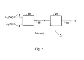
- FIG. 1 of the accompanying drawings is a generalized schematic depiction of a two-stage wavelength converter employing either XPM or XGM, as exemplified by a number of prior art devices.
- the generic prior art wavelength converter comprises a first stage 10 connected to an input 12 for receiving a first optical signal of a first frequency f 1 (or wavelength ⁇ 1 ) and to a further input 14 for receiving a second optical signal of a second frequency f 2 (or wavelength ⁇ 2 ).
- the first stage 10 comprises some kind of nonlinear medium for inducing XPM or XGM of the first signal by the second signal, thereby transferring any intensity modulation contained in the second signal to the first signal.
- the first optical signal is input as a continuous wave (CW) signal, that may be termed a carrier signal
- the second optical signal is input as a data carrying intensity modulated (IM) signal, that may be termed a drive signal.
- CW continuous wave
- IM data carrying intensity modulated
- XPM XPM
- SOA single semiconductor optical amplifier
- MZI Mach-Zehnder interferometer
- DSF dispersion shifted fiber
- the device further comprises a second stage 20 having an input connected by an optical path 16 to receive the second optical signal after its XPM from the first stage.
- the purpose of the second stage is to provide a filter that spectrally enhances the output of the first stage to improve signal quality of the data carried by the second optical signal, as measured by some parameter such as bit error rate (BER).
- BER bit error rate
- the second stage exploits the fact that the XPM impresses the IM of the second optical signal onto the first optical signal not only as an IM, but also as a phase modulation (PM), i.e. a chirp.
- the chirp is related to the nonlinear phase shift induced by the XPM.
- the second stage is designed to generate a further IM contribution responsive to the chirp in the first optical signal, and to generate a further IM which sums with the IM already impressed on the first optical signal in the first stage prior to outputting the signal to an output 18.
- the second stage is designed with a linear transfer function.
- the linear transfer function of the second stage transforms the PM into IM in a manner that weights the IM components from the first stage output to flatten the frequency response of the overall device.
- birefringent fiber for XPM [1]
- FBGs fiber Bragg grating
- XGM XGM [7-10]
- loop mirror filter for XPM [4-6].
- a device for intensity modulating an optical data signal comprising:
- the phase shift retained by the wavelength converted optical signal after the first stage is used in the second stage to obtain a second intensity modulation, synchronous to the intensity modulation imposed by first stage.
- the combined transfer function of the two stages is the product of the individual transfer functions of the two stages, which provides a steeper rising edge to the combined transfer function. This effect can be used, for example, to improve reshaping during wavelength conversion of RZ data.
- the invention starts from a different perspective from the prior art such as the approach of Mahgerefteh and co-workers [8, 11, 23].
- the aim is to enlarge the equivalent bandwidth of a non-linear element used in the first stage which has a relatively low frequency response that limits the operation of the device (e.g. SOA or MZI).
- SOA or MZI limits the operation of the device
- the prior art thus starts from the perspective of wanting to improve the inherently slow frequency response of a single stage wavelength converter.
- the prior art addresses this speed limitation by adding a second stage that acts as a high pass filter and has a linear transfer function defined by the enhancement factor of the first stage non-linear element.
- the present invention starts from the assumption that the first stage may be a fast response component, say with a frequency response greater than 10 Gbit/s, in which case the first stage frequency response is not limiting device performance.
- a fast first stage may be provided by a relatively slow non-linear element such as a SOA arranged in a fast response configuration, such as a semiconductor laser amplifier in a loop optical mirror - SLALOM.
- a fast first stage may be provided by an inherently fast non-linear effect, such as the Kerr-effect, for example a section of non-linear optical fiber).
- the aim of the invention is not to speed up a slow first stage conversion process, as in the prior art, but rather to improve the transfer function of the overall device by making it steeper and more time confined.
- This is achieved according to the invention by combining first and second stages to impress congruent non-inverting intensity modulations on an optical signal traversing the device, with the second stage using residual PM from the first stage to perform its non-inverting IM synchronously with that performed in the first stage.
- the second stage exploits the time derivative of the phase, i.e. frequency shift, it will operate on RZ format signal: independently of the bit value, where each transition between adjacent bits corresponds to a phase transition. This phase transition is associated with a non-zero instant frequency deviation, which is exploited in the second stage.
- the second stage is arranged separate from the first stage, to act on the first optical signal subsequent to output of the first optical signal from the first stage. In other embodiments, the second stage is arranged within the first stage in series with the non-linear optical element.
- the second stage has a transfer function (frequency versus transmission curve) that has a low transmission value (T low ) at the first frequency ( ⁇ 1 /2 ⁇ ) and a high transmission value (T high ) at a frequency equal to the first frequency plus the maximum instantaneous frequency deviation ( ⁇ 1 /2 ⁇ + ⁇ f max ).
- the low transmission value is preferably substantially zero when the first and second stages are separate from each other, but is preferably non-zero when the second stage is arranged as a part of the first stage.
- the second stage can be expected to provide some benefit so long as the range spanning the carrier frequency and the maximum instantaneous frequency deviation ( ⁇ 1 /2 ⁇ + ⁇ f max ) covers at least a significant fraction of the frequency range between minimum and maximum transmission values of the transfer function of the second stage.
- the transfer function has a frequency width ⁇ defined between a minimum transmission value at the first frequency ( ⁇ 1 /2 ⁇ ) and a maximum transmission value (T max ) at frequencies greater than the first frequency plus the frequency width ( ⁇ 1 /2 ⁇ + ⁇ ), then the first and second stages should be matched so that the high transmission value is equal to a significant fraction of the maximum transmission value, for example at least one half of the maximum transmission value (T high ⁇ 0.5T max ), or some other intermediate fraction such as one quarter or three quarters.
- This can be quantified by stating that, if the transfer function has a frequency width ⁇ defined between a minimum transmission value at the first frequency ( ⁇ 1 /2 ⁇ ) and a maximum transmission value (T max ) at frequencies greater than the first frequency plus the frequency width ( ⁇ 1 /2 ⁇ + ⁇ ), then the first and second stages should be matched so that ⁇ ⁇ ⁇ f max , whereby the high transmission value attains the maximum transmission value (T high T max ).
- the transfer function preferably has a non-linear section between the first frequency ( ⁇ 1 /2 ⁇ ) and the maximum instantaneous frequency deviation ( ⁇ 1 /2 ⁇ + ⁇ f max ), thereby to steepen the rise time of the global transfer function of the two-stages viewed collectively.
- Another option is to provide a transfer function with a step like shape, rising almost instantaneously from the low to high transmission values with a near-infinite gradient.
- a pure step filter shape is not practically achievable, but a near step-like shape may be implemented.
- the non-linear optical element may be a semiconductor optical amplifier (SOA), or any other component that provides a non-linear gain medium.
- SOA semiconductor optical amplifier
- the non-linear optical element may be a section of non-linear optical fiber, or any other component that can support the Kerr effect.
- the first stage can have a variety of configurations.
- the first stage has a Sagnac interferometer configuration comprising a loop in which the non-linear optical element is asymmetrically arranged.
- the first stage has a MZI configuration comprising first and second arms having differing path lengths, the non-linear optical element being arranged in the second arm and a further non-linear optical element being arranged in the first arm.
- the path lengths in the two arms of the MZI are only slightly different in order to take advantage of the cancellation of the slow response decay contributions from the non-linear optical element.
- the path lengths will typically be less than 1 cm for 10 Gbit/s data transmission.
- the propagation time associated with the path length difference will be less than the response time of the non-linear optical element (e.g. carrier lifetime of a SOA).
- the first stage preferably either exploits a fast nonlinear effect (e.g. the Kerr effect) or employs a fast nonlinear architecture (e.g. a semiconductor laser amplifier loop optical mirror (SLALOM) or a symmetric Mach-Zehnder interferometer (SMZ).
- a fast nonlinear architecture e.g. a semiconductor laser amplifier loop optical mirror (SLALOM) or a symmetric Mach-Zehnder interferometer (SMZ).
- SLALOM semiconductor laser amplifier loop optical mirror
- SZ symmetric Mach-Zehnder interferometer
- the second stage non-linear filter can have a variety of forms.
- the non-linear filter may have a Sagnac interferometer configuration comprising a length of polarization maintaining optical fiber.
- the non-linear filter may comprise a fiber Bragg grating or a ring resonator device.
- the device operates as a wavelength converter when the input probe signal is CW and the drive signal is intensity modulated with RZ data.
- the device operates as a demultiplexer for optical time division multiplexed (OTDM) signals when the input probe signal is intensity modulated with RZ data and the drive signal is an intensity modulated clock source operating at a bit rate, which will in general be lower than the data rate by a fraction which will usually correspond to the number of OTDM channels.
- OTDM optical time division multiplexed
- the sharp edged transfer function that can be provided by the invention is especially important for OTDM.
- the device may operate with the first and second frequencies equal to each other. To filter out the drive signal prior to the second stage, polarization diversity may be used.
- a method of intensity modulating an optical data signal comprising:
- a method of wavelength converting a return-zero (RZ) optical signal comprising:
- a method of demultiplexing a time division multiplexed return-zero (RZ) optical signal comprising:
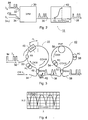
- Figure 2 shows a wavelength converter 15 according to a first embodiment of the invention comprising first and second stages 30 and 40.
- the first stage 30 has an input 34 for receiving a first optical signal of a first frequency f 1 (or wavelength ⁇ 1 or angular velocity ⁇ 1 ) and a further input 32 for receiving a second optical signal of a second frequency f 2 (or wavelength ⁇ 2 or angular velocity ⁇ 2 ).
- the first optical signal is typically continuous wave (CW), and can be termed a carrier or probe signal
- the second optical signal carries a data stream by intensity modulation (IM), and can be termed a data signal.
- the first stage 30 comprises a non-linear element and uses cross phase modulation (XPM) to impress the IM from the data signal onto the CW carrier signal.
- the transfer of the IM data is not perfect, as indicated schematically in the figure by the rounded peaks at the output side of the first stage 30.
- the XPM process also impresses a phase modulation (PM) onto the carrier signal that is related to the IM in the data signal.
- This PM is associated with a frequency range from the probe frequency f 1 to a slightly higher frequency f 1 + ⁇ f max , where ⁇ f max is the maximum instantaneous frequency deviation induced in the probe signal by the XPM.
- the PM exploited by the device can thus be thought of as the positive component of the chirp covering the range f 1 ⁇ f 1 + ⁇ f max (the negative chirp component is not used).
- This secondary PM effect is exploited in a second stage 40 of the device, as now described.
- the second stage 40 is connected to receive the output from the first stage through an optical connection 36.
- the second stage 40 has a non-linear transfer function and serves to impress a further IM on the first optical signal, after the cross phase modulation in the first stage. (The transfer function may be linear in other embodiments).
- the further IM is driven by the PM impressed on the first optical signal in the first stage.
- the transfer function has functional form that ensures that the second IM generation of the second stage combines with that of the first stage to improve the correspondence between the ⁇ 2 -IM in the drive signal and the wavelength converted ⁇ 1 -IM signal output from the device through an output 38.
- the transfer function takes the form of a supralinearly rising edge, rising over the chirp range of the first stage PM, i.e. over f 1 ⁇ f 1 + ⁇ f max or ⁇ 1 ⁇ ⁇ 1 + 2 ⁇ f max .
- the second stage thus takes advantage of the frequency chirp associated with PM still impressed on the probe signal exiting first stage to operate a further intensity modulation synchronous with the previous one.
- the obtained cascaded device displays improved reshaping properties and simultaneously offers high-speed operation.
- Figure 3 shows a specific example of the wavelength converter of Figure 2 in which the first and second stages are both based on a Sagnac interferometer configuration.
- the first stage 30 is a so-called “semiconductor laser amplifier in a loop optical mirror” (SLALOM) device [12], also known as a “terahertz optical asymmetric demultiplexer” (TOAD) device [13].
- the SLALOM comprises a waveguide loop forming an optical loop mirror with light being coupled in and out by a waveguide coupler 48, which is a 50/50 coupler in this example.
- the waveguide coupler is connected to the probe signal input 34 to couple the probe signal into the waveguide loop.
- the probe signal traverses the loop as two components traveling clockwise (CKW) and counterclockwise (CKW), the components having equal power in the case of a 50/50 waveguide coupler 48.
- CKW traveling clockwise
- CKW counterclockwise
- the components having equal power in the case of a 50/50 waveguide coupler 48.
- SOA semiconductor optical amplifier
- the center offset is indicated with the parameter ⁇ L.
- the purpose of the offset is to ensure that the CCKW component passes through the SOA after the SOA has been passed by the CKW component (or vice versa).
- PC polarization controller
- To couple in the data signal into the loop there is provided a further coupler 44 connected to the input 32, for example with a 90/10 coupling ratio.
- the SLALOM topology offers advantages such as low control pulse energy and compactness, no dispersion and no walk-off.
- a drawback in comparison with embodiments using a non-linear optical loop mirror (NOLM) topology is that operation speed is relatively limited by inherent SOAs carrier lifetime.
- NOLM non-linear optical loop mirror
- other SLALOM types may be used, some variations being described in reference [12] the contents of which are incorporated herein by reference.
- the SLALOM has a switching window determined principally by two factors, namely the SOAs displacement ⁇ L with reference to the loop center and its gain recovery time, which is of the order of hundreds of picoseconds.
- the wavelength conversion function requires careful positioning of the SOA near the loop center, to avoid degradation due to a known patterning effect [14].
- the Sagnac interferometer transmittance, T(t), of the first stage is due to interplay of both XPM and XGM in the SOA (although the XGM contribution is small) and is expressed by the following equation, for the optimum 3 dB input coupling ratio [12]: where G(t) and G(t-2 ⁇ t) are the gain experienced by the clockwise and counterclockwise probe signal components respectively.
- the parameter ⁇ t n ⁇ L/c corresponds to half the delay between the two probe components.
- the parameter ⁇ is the linewidth enhancement factor, which expresses the SOAs relation between nonlinear phase modulation and nonlinear gain compression.
- the IM and PM probe signal then exits the first stage and is channeled to the second stage.
- a tunable bandpass filter 42 is arranged in the connection path 36 between the first and second stages to filter out the data signal wavelength ⁇ 2 .
- the second stage 40 is based on a polarization maintaining fiber (PMF) optical loop [4-6], which is another device based on a Sagnac interferometer configuration.
- the second stage comprises an optical loop including a length of PMF 56, two sets of polarization controllers 54 and 58 arranged either side of the PMF 56 and a coupler 52, indicated as having a 50/50 coupling ratio, for coupling the probe signal into and out of the loop.
- the input signal is split into two components by the coupler 52 which traverse the loop in opposite directions, i.e. as CKW and CCKW components.
- the PMF 56 in the second stage provides a transfer function with a transmission minimum at the probe frequency and a higher transmission, preferably a maximum, at the probe frequency plus the maximum instantaneous positive frequency shift induced in the first stage.
- the transmission notch of the second stage is thus tuned to the probe frequency. In this way, a further conversion is obtained in the second stage that is synchronous with the first stage conversion.
- Figure 4 shows the transfer function of the PMF optical loop second stage.
- the cyclical nature of the transfer function, attributable to the interferometric operation, is evident.
- the second stage is tuned to operate on the leading edge of one of the transfer function periods.
- the maximum instantaneous frequency deviation of the first stage should not amount to more than one half cycle in the transfer function of the second stage.
- the SOA 46 is an Opto-Speed 1550MRI/P device, 750- ⁇ m long and polarization independent. It is off-centered by ⁇ L ⁇ 2 cm.
- the IM drive signal source is an RZ-externally modulated distributed feedback (DFB) laser having an operating wavelength of 1559.5 nm.
- the CW probe signal source is a Photonetics tunable external cavity laser (ECL) which was operated at 1545 nm to obtain the results described herein.
- ECL Photonetics tunable external cavity laser
- the PMF 56 is a 10 m length of Fujikura SM-15-P-8 fiber with an ⁇ n of 3 ⁇ 10 -4 resulting in a group differential delay of 1 ps/nm and in a 62 GHz-filter function (see Figure 4).
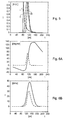
- Figure 5 shows first stage output switching window for different possible shapes of drive signal pulses, namely rectangular (I), raised cosine (II) and gaussian (III).
- ⁇ t corresponding to the physical SOA displacement in the loop ⁇ L, is a good indication of the 3 dB window duration, different pulse shapes may have differently effects on the output window shape and duration.
- FIGS 6A and 6B show respectively phase and frequency transfer function of the SLALOM for a gaussian drive pulse, using the same parameter values as in the preceding figure.
- the SLALOM switching window is also displayed (dashed lines).
- the maximum instantaneous frequency deviation, ⁇ f max corresponds to the first stage switching window.
- the design of the second stage needs to take into account the maximum nonlinear frequency shift ⁇ f max imposed in the first stage, in that two subsequent minima (maxima) in the transfer function of the second stage should be separated in frequency by more than the ⁇ f max value. Further, the frequency difference ⁇ between the maximum and minimum of the transfer function is optimized when it is less than or equal to ⁇ f max , although useful operation with higher losses can still be obtained with ⁇ > ⁇ f max .
- the cascade of the two transfer functions of the two stages has the net result of enhancing the extinction ratio and also compressing the pulses.
- Figure 7A shows the switching window of the first stage only (I), and of the combined first and second stages (II), for the specific example of the first embodiment.
- the pulse compression effect of the second stage is evident by the narrower window obtained after the second stage.
- Figure 7B shows, for comparison, the switching window of the first stage only (I), and of the combined first and second stages (II), according to an alternate embodiment where the second stage is a cubic filter.
- the steeper rising edge of the transfer function of a cubic filter can be expected to further improve the pulse compression.
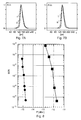
- Figure 8 shows experimental bit error rate (BER) data taken from a device according to the specific example of the first embodiment at the input of the first stage (circles) and at the output of the second stage (squares).
- BER bit error rate
- FIG. 9 shows the wavelength converter or the first embodiment, or any of the further embodiments described below, in a system context as part of an optical cross connect (OXC) for WDM signals.
- the OXC comprises a bank 140 of wavelength converters 15 on the output side of respective banks 130 of space switching matrices which receive signals from respective banks of tunable filters 120.
- Input and output side erbium doped fiber amplifier (EDFA) banks 100 and 150 are also provided. Operation of the OXC, and also a local add and drop function, is controlled by a digital controller 110.
- the wavelength converters 15 are used by the controller 110 to resolve contentions between input signals of the same wavelength that are to be routed to the same output waveguide.
- the OXC is an important routing component for optical networks.
- Figure 10 shows a wavelength converter according to a second embodiment.
- the device of the second embodiment may be considered to be the same as that of the first embodiment, except that for the first stage the SOA is replaced with non-linear fiber section 47.
- the SLALOM first stage is replaced with a NOLM first stage.
- This wavelength converter device is thus based on XPM induced by the Kerr effect in a non-linear medium provided by an optical fiber.
- a high power IM laser is used with a CW probe.
- the CCKW phase shift is constant, while the CKW phase shift follows the pump IM with a very high speed of response that is associated with the Kerr effect.
- This nonlinear phase is read by the second stage and transformed into IM, which results in more close replication of the pump IM in the wavelength converted signal.
- the probe retains a frequency chirping associated to this nonlinear PM, whose shape is a square wave.
- the time derivative of this phase shift is read by the second stage filter, whose notch is tuned to the carrier frequency, while positive chirping moves the second stage output to a high value.
- the second stage is shown in generic fashion.
- the second stage may be a PMF optical loop as used in the specific example of the first embodiment.
- Figure 11 shows a wavelength converter according to a third embodiment in which the first stage 30 is a symmetric Mach-Zehnder (SMZ) interferometer [17-19].
- the probe signal is coupled into each arm 66, 68 of the interferometer by a coupler 62.
- the drive signal is also coupled into each arm 66, 68 of the interferometer by further couplers 74, 76, 78.
- SOAs 70 and 72 for inducing the desired XPM are arranged in the arms 66 and 68 respectively.
- the signal components in the arms are then interferometrically combined in a coupler 64 and routed to the second stage 40 which is as described in relation to the preceding embodiments.
- the SMZ interferometer has a transfer function similar to that of a SLALOM, while not performing common mode noise rejection.
- the IM pump is split and fed to both interferometer arms.
- the signal component passing through the first and second arms play the role of the CKW and CCKW signal components in a SLALOM first stage.
- the SOAs in the two arms are the same and also biased the same.
- the nonlinear phase shift induced by the SOAs in the two equal signal components of the CW probe signal is thus equal, although time delayed due to a path imbalance between the first and second arms.
- the SMZ configuration therefore has similar behavior to the SLALOM configuration in respect of the output intensity transfer function and the output signal phase.
- Figure 12 shows a wavelength converter according to a fourth embodiment in which the second stage 40 is incorporated as part of the first stage 30.
- the first stage 30 is based on a SLALOM configuration similar to that of the first embodiment, but with the second stage inserted into the side of the loop that receives the CCKW signal component first from the coupler 48.
- the second stage filter transmission notch is purposely tuned next to the carrier frequency (in this configuration more losses have to be accepted).
- the CCKW probe signal component passes through the filter before being nonlinearly phase modulated, and thus propagates with unchanged profile, but attenuated, through the second stage filter.
- the CKW probe signal component enters the filter after propagating through the SOA 46 and the filter 40 reads its frequency chirp, thus modulating its intensity.
- the filter function IM then takes place before the CKW and CCKW signal components recombine.
- the beneficial cascaded effect still occurs since the total transfer function is still proportional to the product between CKW and CCKW amplitudes and the sine of the phase difference between the CKW and CCKW signal components.
- Figure 13 shows operation of the device of Figure 12.
- the upper trace shows the amplitudes of the clockwise (CKW) probe signal component (dashed line) and the counterclockwise (CCKW) probe signal component (solid line - constant baseline).
- the middle trace shows the nonlinear phases of the CKW probe signal component (dashed line) and the CCKW probe signal component (solid line).
- the lower trace shows the switching window due to the nonlinear phase differences alone (continuous wave) and the product of the two amplitudes shown in the upper trace (dashed lines).
- the whole transfer function is given as the product of the switching window defined by the nonlinear phase differences and the amplitudes of the clockwise and counterclockwise probe signal components.
- Figure 14 shows a wavelength converter according to a fifth embodiment. This device is similar to that of Figure 12, but with the SOA replaced with a non-linear optical fiber.
- Figure 15 shows a wavelength converter according to a sixth embodiment.
- This embodiment has the SMZ structure of the embodiment of Figure 11, but with the second stage filter 40 arranged as part of the first stage in an arm of the SMZ.
- Figure 16 shows a demultiplexer according to a seventh embodiment for demultiplexing an optical time division multiplexed (OTDM) signal.
- the structure is the same as in Figure 2, but the input signals are different.
- the probe signal at ⁇ 1 carries IM data, in the form of OTDM RZ.
- the ⁇ 1 signal carries an IM clock signal.
- the first stage 30 effectively imposes the envelope of the clock signal onto the OTDM data signal, selecting out particular time slot in each OTDM period to provide an output signal OP, thereby acting as a demultiplexer.
- the first stage output signal OP is then fed into the second stage 40 and modified to provide an enhanced output signal OP' similar to the wavelength converter embodiments.
- FIGS 17A-D show example clock (CLK), NRZ data (DATA), first stage output (OP) and second stage output (OP') signals for the seventh embodiment.
- CLK clock
- DATA NRZ data
- OP first stage output
- OP' second stage output
- one OTDM channel is selected out of the NRZ data by the clock signal.
- a different channel can be selected by introducing a phase shift to the clock signal.
- multiple OTDM channels may be filtered out if desired through an appropriate choice of clock signal.
- the reshaping and time compression effects of the second stage are indicated schematically by the illustrated pulse shapes.
- the device can also perform demultiplexing on RZ data.
Landscapes
- Physics & Mathematics (AREA)
- Nonlinear Science (AREA)
- General Physics & Mathematics (AREA)
- Optics & Photonics (AREA)
- Engineering & Computer Science (AREA)
- Power Engineering (AREA)
- Optical Modulation, Optical Deflection, Nonlinear Optics, Optical Demodulation, Optical Logic Elements (AREA)
Abstract
Description
- The invention relates to intensity modulation of optical signals, more especially but not exclusively to wavelength converters and demultiplexers of optical signals carrying data encoded by intensity modulation.
- A typical wavelength converter transfers an intensity modulation in a first signal of a first wavelength to a second signal of a second wavelength. This is useful for converting return zero (RZ) or non-return-zero (NRZ) data from one wavelength to another wavelength, as is a generally useful in a wavelength division multiplexed (WDM) environment, for example for an optical cross connect (OXC).
- It is known that a wavelength converter can be based on cross phase modulation (XPM) or cross gain modulation (XGM) in a nonlinear medium, such as a semiconductor optical amplifier (SOA) or nonlinear optical fiber.
- Figure 1 of the accompanying drawings is a generalized schematic depiction of a two-stage wavelength converter employing either XPM or XGM, as exemplified by a number of prior art devices.
- The generic prior art wavelength converter comprises a
first stage 10 connected to aninput 12 for receiving a first optical signal of a first frequency f1 (or wavelength λ1) and to afurther input 14 for receiving a second optical signal of a second frequency f2 (or wavelength λ2). Thefirst stage 10 comprises some kind of nonlinear medium for inducing XPM or XGM of the first signal by the second signal, thereby transferring any intensity modulation contained in the second signal to the first signal. Typically the first optical signal is input as a continuous wave (CW) signal, that may be termed a carrier signal, and the second optical signal is input as a data carrying intensity modulated (IM) signal, that may be termed a drive signal. - Various different components have been used in the prior art to provide XPM in the first stage. Examples are a single semiconductor optical amplifier (SOA) for XPM [1-3] or XGM [7-10, 22], a Mach-Zehnder interferometer (MZI) with SOAs in each arm for XPM [11, 23], and dispersion shifted fiber (DSF) for XPM [4-6].
- The device further comprises a
second stage 20 having an input connected by anoptical path 16 to receive the second optical signal after its XPM from the first stage. The purpose of the second stage is to provide a filter that spectrally enhances the output of the first stage to improve signal quality of the data carried by the second optical signal, as measured by some parameter such as bit error rate (BER). (It is noted that a simple wavelength converter will have no second stage and thus consist only of the above described first stage.) The second stage exploits the fact that the XPM impresses the IM of the second optical signal onto the first optical signal not only as an IM, but also as a phase modulation (PM), i.e. a chirp. The chirp is related to the nonlinear phase shift induced by the XPM. The second stage is designed to generate a further IM contribution responsive to the chirp in the first optical signal, and to generate a further IM which sums with the IM already impressed on the first optical signal in the first stage prior to outputting the signal to anoutput 18. - To increase the effective frequency response of the first stage, the second stage is designed with a linear transfer function. The linear transfer function of the second stage transforms the PM into IM in a manner that weights the IM components from the first stage output to flatten the frequency response of the overall device.
- Various different components have been used in the prior art for the second stage. Examples are birefringent fiber for XPM [1], a fiber Bragg grating (FBGs) for XPM [2, 3, 11, 24] or XGM [7-10], and a loop mirror filter for XPM [4-6].
- In summary, a variety of two stage devices have been proposed for wavelength conversion that are based on XPM and XGM. Several of these devices use the PM generated in a wavelength converting first stage to drive a second stage, the second stage having a linear transfer function that compensates for the inherently slow frequency response in the first stage.
- According to a first aspect of the invention there is provided a device for intensity modulating an optical data signal, the device comprising:
- a first stage arranged to impress an intensity modulation that is non-inverting as well as a phase modulation on a first optical signal of a first frequency responsive to an intensity modulation carried by a second optical signal of a second frequency using cross phase modulation in a non-linear optical element; and
- a second stage arranged to impress a further intensity modulation that is non-inverting on the first optical signal, after the cross phase modulation, responsive to the phase modulation impressed on the first optical signal in the first stage.
-
- In use, the phase shift retained by the wavelength converted optical signal after the first stage is used in the second stage to obtain a second intensity modulation, synchronous to the intensity modulation imposed by first stage. The combined transfer function of the two stages is the product of the individual transfer functions of the two stages, which provides a steeper rising edge to the combined transfer function. This effect can be used, for example, to improve reshaping during wavelength conversion of RZ data.
- The invention starts from a different perspective from the prior art such as the approach of Mahgerefteh and co-workers [8, 11, 23].
- In the prior art, the aim is to enlarge the equivalent bandwidth of a non-linear element used in the first stage which has a relatively low frequency response that limits the operation of the device (e.g. SOA or MZI). The prior art thus starts from the perspective of wanting to improve the inherently slow frequency response of a single stage wavelength converter. The prior art addresses this speed limitation by adding a second stage that acts as a high pass filter and has a linear transfer function defined by the enhancement factor of the first stage non-linear element.
- By contrast, the present invention starts from the assumption that the first stage may be a fast response component, say with a frequency response greater than 10 Gbit/s, in which case the first stage frequency response is not limiting device performance. (A fast first stage may be provided by a relatively slow non-linear element such as a SOA arranged in a fast response configuration, such as a semiconductor laser amplifier in a loop optical mirror - SLALOM. Alternatively, a fast first stage may be provided by an inherently fast non-linear effect, such as the Kerr-effect, for example a section of non-linear optical fiber). The aim of the invention is not to speed up a slow first stage conversion process, as in the prior art, but rather to improve the transfer function of the overall device by making it steeper and more time confined. This is achieved according to the invention by combining first and second stages to impress congruent non-inverting intensity modulations on an optical signal traversing the device, with the second stage using residual PM from the first stage to perform its non-inverting IM synchronously with that performed in the first stage.
- As the second stage exploits the time derivative of the phase, i.e. frequency shift, it will operate on RZ format signal: independently of the bit value, where each transition between adjacent bits corresponds to a phase transition. This phase transition is associated with a non-zero instant frequency deviation, which is exploited in the second stage.
- In some embodiments, the second stage is arranged separate from the first stage, to act on the first optical signal subsequent to output of the first optical signal from the first stage. In other embodiments, the second stage is arranged within the first stage in series with the non-linear optical element.
- In preferred embodiments, the second stage has a transfer function (frequency versus transmission curve) that has a low transmission value (Tlow) at the first frequency (ω1/2π) and a high transmission value (Thigh) at a frequency equal to the first frequency plus the maximum instantaneous frequency deviation (ω1/2π + Δfmax).
- The low transmission value is preferably substantially zero when the first and second stages are separate from each other, but is preferably non-zero when the second stage is arranged as a part of the first stage.
- The second stage can be expected to provide some benefit so long as the range spanning the carrier frequency and the maximum instantaneous frequency deviation (ω1/2π + Δfmax) covers at least a significant fraction of the frequency range between minimum and maximum transmission values of the transfer function of the second stage.
- This can be quantified by stating that, if the transfer function has a frequency width Δν defined between a minimum transmission value at the first frequency (ω1/2π) and a maximum transmission value (Tmax) at frequencies greater than the first frequency plus the frequency width (ω1/2π + Δν), then the first and second stages should be matched so that the high transmission value is equal to a significant fraction of the maximum transmission value, for example at least one half of the maximum transmission value (Thigh ≥ 0.5Tmax), or some other intermediate fraction such as one quarter or three quarters.
- For best operation, the full transmission range of the second stage should be exploited.
- This can be quantified by stating that, if the transfer function has a frequency width Δν defined between a minimum transmission value at the first frequency (ω1/2π) and a maximum transmission value (Tmax) at frequencies greater than the first frequency plus the frequency width (ω1/2π + Δν), then the first and second stages should be matched so that Δν ≤ Δfmax, whereby the high transmission value attains the maximum transmission value (Thigh = Tmax).
- The transfer function preferably has a non-linear section between the first frequency (ω1/2π) and the maximum instantaneous frequency deviation (ω1/2π + Δfmax), thereby to steepen the rise time of the global transfer function of the two-stages viewed collectively.
- Another option is to provide a transfer function with a step like shape, rising almost instantaneously from the low to high transmission values with a near-infinite gradient. Clearly, a pure step filter shape is not practically achievable, but a near step-like shape may be implemented.
- A variety of components may be used for the non-linear optical element. For example, the non-linear optical element may be a semiconductor optical amplifier (SOA), or any other component that provides a non-linear gain medium. The non-linear optical element may be a section of non-linear optical fiber, or any other component that can support the Kerr effect.
- The first stage can have a variety of configurations. In one example, the first stage has a Sagnac interferometer configuration comprising a loop in which the non-linear optical element is asymmetrically arranged. In another example, the first stage has a MZI configuration comprising first and second arms having differing path lengths, the non-linear optical element being arranged in the second arm and a further non-linear optical element being arranged in the first arm. In this example, the path lengths in the two arms of the MZI are only slightly different in order to take advantage of the cancellation of the slow response decay contributions from the non-linear optical element. For example, the path lengths will typically be less than 1 cm for 10 Gbit/s data transmission. In other words, the propagation time associated with the path length difference will be less than the response time of the non-linear optical element (e.g. carrier lifetime of a SOA).
- The first stage preferably either exploits a fast nonlinear effect (e.g. the Kerr effect) or employs a fast nonlinear architecture (e.g. a semiconductor laser amplifier loop optical mirror (SLALOM) or a symmetric Mach-Zehnder interferometer (SMZ).
- The second stage non-linear filter can have a variety of forms. For example, the non-linear filter may have a Sagnac interferometer configuration comprising a length of polarization maintaining optical fiber. Alternatively, the non-linear filter may comprise a fiber Bragg grating or a ring resonator device.
- In one set of applications, the device operates as a wavelength converter when the input probe signal is CW and the drive signal is intensity modulated with RZ data.
- In another set of applications, the device operates as a demultiplexer for optical time division multiplexed (OTDM) signals when the input probe signal is intensity modulated with RZ data and the drive signal is an intensity modulated clock source operating at a bit rate, which will in general be lower than the data rate by a fraction which will usually correspond to the number of OTDM channels. The sharp edged transfer function that can be provided by the invention is especially important for OTDM. In the case of the demultiplexing application the device may operate with the first and second frequencies equal to each other. To filter out the drive signal prior to the second stage, polarization diversity may be used.
- According to a second aspect of the invention there is provided a method of intensity modulating an optical data signal, the method comprising:
- (a) impressing an intensity modulation that is non-inverting, as well as a phase modulation, on a first optical signal responsive to an intensity modulation carried by a second optical signal, using cross phase modulation; and
- (b) impressing a further intensity modulation that is non-inverting on the first optical signal, after the cross phase modulation, responsive to said phase modulation.
-
- According to a further aspect of the invention there is provided a method of wavelength converting a return-zero (RZ) optical signal, the method comprising:
- (a) receiving a first optical signal at a first frequency (ω1/2π);
- (b) receiving a second optical signal at a second frequency carrying RZ intensity modulated data;
- (c) impressing an intensity modulation that is non-inverting, as well as a phase modulation, on the first optical signal by cross phase modulation with the second optical signal, wherein the intensity modulation carries the data, and the phase modulation is associated with a maximum instantaneous frequency deviation (Δfmax); and
- (d) impressing a further intensity modulation that is non-inverting on the first optical signal, after the cross phase modulation, responsive to said phase modulation.
-
- According to a still further aspect of the invention there is provided a method of demultiplexing a time division multiplexed return-zero (RZ) optical signal, comprising:
- (a) receiving a first optical signal at a first frequency (ω1/2π) carrying RZ intensity modulated data organized in time slots for respective time division multiplexed channels;
- (b) receiving a second optical signal at a second frequency carrying a sequence of intensity modulated clock pulses;
- (c) impressing an intensity modulation that is non-inverting, as well as a phase modulation, on the first optical signal by cross phase modulation with the second optical signal, wherein the intensity modulation serves to select at least one of the time slots, and the phase modulation is associated with a maximum instantaneous frequency deviation (Δfmax); and
- (d) impressing a further intensity modulation that is non-inverting on the first optical signal, after the cross phase modulation, responsive to said phase modulation.
-
- For a better understanding of the invention and to show how the same may be carried into effect reference is now made by way of example to the accompanying drawings in which:
- Figure 1 shows a general prior art two stage wavelength converter;
- Figure 2 shows a two stage wavelength converter according to a first embodiment of the invention;
- Figure 3 shows a specific example of the wavelength converter of Figure 2;
- Figure 4 is a graph showing the transfer function of the second stage of the wavelength converter of Figure 3;
- Figure 5 shows the output switching window of the first stage of the first embodiment for three different IM drive pulse shapes;
- Figure 6A shows the phase transfer function of the first stage of the first embodiment for a gaussian IM drive pulse shape, the first stage switching window also being shown (dashed line);
- Figure 6B shows the frequency transfer function of the first stage of the first embodiment for a gaussian IM drive pulse shape, the first stage switching window also being shown (dashed line);
- Figure 7A shows the switching window of the first stage only (I), and of the combined first and second stages (II), for the first embodiment;
- Figure 7B shows the switching window of the first stage only (I), and of the combined first and second stages (II), according to an alternate embodiment where the second stage is a cubic filter;
- Figure 8 shows experimental bit error rate (BER) data taken from a device according to the first embodiment at the input of the device (circles) and at the output of the device (squares);
- Figure 9 shows an optical cross connect (OXC) employing wavelength converters according to embodiments of the invention;
- Figure 10 shows a wavelength converter according to a second embodiment;
- Figure 11 shows a wavelength converter according to a third embodiment;
- Figure 12 shows a wavelength converter according to a fourth embodiment in which the second stage is incorporated as part of the first stage;
- Figure 13 shows operation of the device of Figure 12;
- Figure 14 shows a wavelength converter according to a fifth embodiment;
- Figure 15 shows a wavelength converter according to a sixth embodiment;
- Figure 16 shows a demultiplexer according to a seventh embodiment for demultiplexing an optical time division multiplexed (OTDM) signal; and
- Figures 17A-D show example clock, data, intermediate and output signals for the seventh embodiment.
-
- Figure 2 shows a
wavelength converter 15 according to a first embodiment of the invention comprising first andsecond stages - The
first stage 30 has aninput 34 for receiving a first optical signal of a first frequency f1 (or wavelength λ1 or angular velocity ω1) and afurther input 32 for receiving a second optical signal of a second frequency f2 (or wavelength λ2 or angular velocity ω2). For operation as a wavelength converter, the first optical signal is typically continuous wave (CW), and can be termed a carrier or probe signal, and the second optical signal carries a data stream by intensity modulation (IM), and can be termed a data signal. Thefirst stage 30 comprises a non-linear element and uses cross phase modulation (XPM) to impress the IM from the data signal onto the CW carrier signal. The transfer of the IM data is not perfect, as indicated schematically in the figure by the rounded peaks at the output side of thefirst stage 30. The XPM process also impresses a phase modulation (PM) onto the carrier signal that is related to the IM in the data signal. This PM is associated with a frequency range from the probe frequency f1 to a slightly higher frequency f1 + Δfmax , where Δfmax is the maximum instantaneous frequency deviation induced in the probe signal by the XPM. The PM exploited by the device can thus be thought of as the positive component of the chirp covering the range f1 → f1 + Δfmax (the negative chirp component is not used). This secondary PM effect is exploited in asecond stage 40 of the device, as now described. - The
second stage 40 is connected to receive the output from the first stage through anoptical connection 36. Thesecond stage 40 has a non-linear transfer function and serves to impress a further IM on the first optical signal, after the cross phase modulation in the first stage. (The transfer function may be linear in other embodiments). The further IM is driven by the PM impressed on the first optical signal in the first stage. The transfer function has functional form that ensures that the second IM generation of the second stage combines with that of the first stage to improve the correspondence between the λ2-IM in the drive signal and the wavelength converted λ1-IM signal output from the device through anoutput 38. As illustrated schematically in the figure, the transfer function takes the form of a supralinearly rising edge, rising over the chirp range of the first stage PM, i.e. over f1 → f1 + Δfmax or ω1 → ω1 + 2πΔfmax. The second stage thus takes advantage of the frequency chirp associated with PM still impressed on the probe signal exiting first stage to operate a further intensity modulation synchronous with the previous one. The obtained cascaded device displays improved reshaping properties and simultaneously offers high-speed operation. - Figure 3 shows a specific example of the wavelength converter of Figure 2 in which the first and second stages are both based on a Sagnac interferometer configuration. More specifically, the
first stage 30 is a so-called "semiconductor laser amplifier in a loop optical mirror" (SLALOM) device [12], also known as a "terahertz optical asymmetric demultiplexer" (TOAD) device [13]. The SLALOM comprises a waveguide loop forming an optical loop mirror with light being coupled in and out by awaveguide coupler 48, which is a 50/50 coupler in this example. The waveguide coupler is connected to theprobe signal input 34 to couple the probe signal into the waveguide loop. The probe signal traverses the loop as two components traveling clockwise (CKW) and counterclockwise (CKW), the components having equal power in the case of a 50/50waveguide coupler 48. In the loop there is arranged slightly off-center a semiconductor optical amplifier (SOA). In the figure, the center offset is indicated with the parameter ΔL. The purpose of the offset is to ensure that the CCKW component passes through the SOA after the SOA has been passed by the CKW component (or vice versa). The loop is also provided with a polarization controller (PC) 50. To couple in the data signal into the loop, there is provided afurther coupler 44 connected to theinput 32, for example with a 90/10 coupling ratio. - The SLALOM topology offers advantages such as low control pulse energy and compactness, no dispersion and no walk-off. A drawback in comparison with embodiments using a non-linear optical loop mirror (NOLM) topology is that operation speed is relatively limited by inherent SOAs carrier lifetime. It will be understood that other SLALOM types may be used, some variations being described in reference [12] the contents of which are incorporated herein by reference. The SLALOM has a switching window determined principally by two factors, namely the SOAs displacement ΔL with reference to the loop center and its gain recovery time, which is of the order of hundreds of picoseconds. Thus, while operation as demultiplexer is easily achieved (demultiplexer action of the device is described further below), the wavelength conversion function requires careful positioning of the SOA near the loop center, to avoid degradation due to a known patterning effect [14].
- The Sagnac interferometer transmittance, T(t), of the first stage is due to interplay of both XPM and XGM in the SOA (although the XGM contribution is small) and is expressed by the following equation, for the optimum 3 dB input coupling ratio [12]:where G(t) and G(t-2Δt) are the gain experienced by the clockwise and counterclockwise probe signal components respectively. The parameter Δt=nΔL/c corresponds to half the delay between the two probe components. The parameter α is the linewidth enhancement factor, which expresses the SOAs relation between nonlinear phase modulation and nonlinear gain compression.

- The probe signal exiting the first stage retains a nonlinear PM (t) to which an instant frequency deviation d(t) / dt is associated:
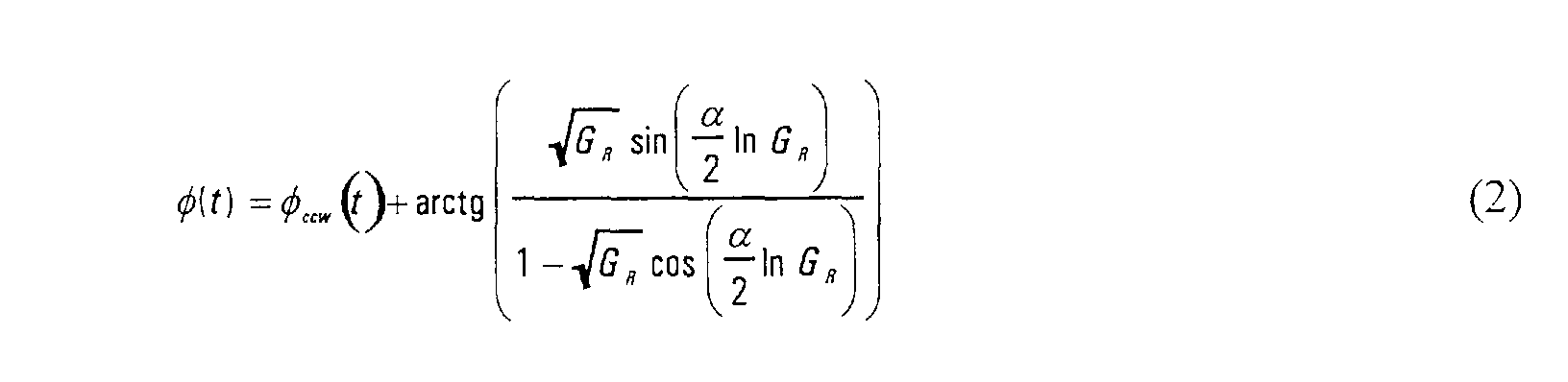 where the apex indicates time derivative ccw is the nonlinear phase shift experienced by the counterclockwise probe signal component and GR is the ratio between G(t) and G(t-2Δt), and dFo(t) / dt is the time derivative of the phase transfer function, F (t) = - m , where in is the initial constant phase of the CW probe signal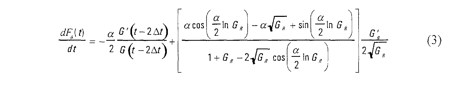
- The IM and PM probe signal then exits the first stage and is channeled to the second stage. A
tunable bandpass filter 42 is arranged in theconnection path 36 between the first and second stages to filter out the data signal wavelength λ2. Thesecond stage 40 is based on a polarization maintaining fiber (PMF) optical loop [4-6], which is another device based on a Sagnac interferometer configuration. The second stage comprises an optical loop including a length ofPMF 56, two sets ofpolarization controllers PMF 56 and acoupler 52, indicated as having a 50/50 coupling ratio, for coupling the probe signal into and out of the loop. As in the first stage, the input signal is split into two components by thecoupler 52 which traverse the loop in opposite directions, i.e. as CKW and CCKW components. - The
PMF 56 in the second stage provides a transfer function with a transmission minimum at the probe frequency and a higher transmission, preferably a maximum, at the probe frequency plus the maximum instantaneous positive frequency shift induced in the first stage. The transmission notch of the second stage is thus tuned to the probe frequency. In this way, a further conversion is obtained in the second stage that is synchronous with the first stage conversion. - Figure 4 shows the transfer function of the PMF optical loop second stage. The cyclical nature of the transfer function, attributable to the interferometric operation, is evident. The second stage is tuned to operate on the leading edge of one of the transfer function periods. In other words, in this example, the maximum instantaneous frequency deviation of the first stage should not amount to more than one half cycle in the transfer function of the second stage.
- In experiments, the following components were used: The
SOA 46 is an Opto-Speed 1550MRI/P device, 750-µm long and polarization independent. It is off-centered by ΔL ≈ 2 cm. The IM drive signal source is an RZ-externally modulated distributed feedback (DFB) laser having an operating wavelength of 1559.5 nm. The CW probe signal source is a Photonetics tunable external cavity laser (ECL) which was operated at 1545 nm to obtain the results described herein. Thetunable bandpass filter 42 between the first and second stages has a 1.3 nm bandpass. ThePMF 56 is a 10 m length of Fujikura SM-15-P-8 fiber with an Δn of 3·10-4 resulting in a group differential delay of 1 ps/nm and in a 62 GHz-filter function (see Figure 4). - Figure 5 shows first stage output switching window for different possible shapes of drive signal pulses, namely rectangular (I), raised cosine (II) and gaussian (III). In all three cases, the parameters used to calculate the switching window profiles shown in the figure are: unperturbed small signal gain G0=100 (20dB); SOA enhancement factor α=4; switching window 2ΔL/vg = 40 ps; bit time of drive signal Tbit=200 ps; and drive pulse energy Uin = 0.05 Usat, where Usat is the SOA saturation energy. It is noted that, although Δt, corresponding to the physical SOA displacement in the loop ΔL, is a good indication of the 3 dB window duration, different pulse shapes may have differently effects on the output window shape and duration.
- Figures 6A and 6B show respectively phase and frequency transfer function of the SLALOM for a gaussian drive pulse, using the same parameter values as in the preceding figure. For the sake of clarity, in both figures the SLALOM switching window is also displayed (dashed lines). As can be seen, the maximum instantaneous frequency deviation, Δfmax corresponds to the first stage switching window.
- The design of the second stage needs to take into account the maximum nonlinear frequency shift Δfmax imposed in the first stage, in that two subsequent minima (maxima) in the transfer function of the second stage should be separated in frequency by more than the Δfmax value. Further, the frequency difference Δν between the maximum and minimum of the transfer function is optimized when it is less than or equal to Δfmax, although useful operation with higher losses can still be obtained with Δν > Δfmax. The cascade of the two transfer functions of the two stages has the net result of enhancing the extinction ratio and also compressing the pulses.
- Figure 7A shows the switching window of the first stage only (I), and of the combined first and second stages (II), for the specific example of the first embodiment. The pulse compression effect of the second stage is evident by the narrower window obtained after the second stage.
- Figure 7B shows, for comparison, the switching window of the first stage only (I), and of the combined first and second stages (II), according to an alternate embodiment where the second stage is a cubic filter. As is evident, the steeper rising edge of the transfer function of a cubic filter, can be expected to further improve the pulse compression.
- Figure 8 shows experimental bit error rate (BER) data taken from a device according to the specific example of the first embodiment at the input of the first stage (circles) and at the output of the second stage (squares). Experiments were performed with a 29-1 PRBS RZ format drive signal at 3 Gbit/s and 5 Gbit/s. Eye diagrams (not shown) were used to compare the converted probe at first stage output and second stage output at a fixed received power P. At 3 Gbit/s, the eye diagrams were open at the output of the first and second stages, with clear pulse compression being visible. At 5 Gbit/s complete eye closure was seen after the first stage, which is attributed to the inherent (about 4 Gbit/s) speed limitation of the SLALOM first stage with ΔL ≈ 2 cm. After the second stage, the eye diagrams were reopened, showing that this limit has been overcome. The results are quantitatively represented in the figure by BER curves for 5 Gbit/s transmission. The
RZ 5 Gbit/s converted signal has a 2.8 dB penalty, partly due to imperfect filter tuning. - In conclusion, successful 5 Gbit/s operation of a two-stage interferometric wavelength converter has been experimentally demonstrated. As will be understood from reference [14], engineering the SOAs position in the first loop will improve the window dimension allowing higher bit rates. Cascading with the second stage provides a steeper transfer function and obtains a reshaped signal.
- Figure 9 shows the wavelength converter or the first embodiment, or any of the further embodiments described below, in a system context as part of an optical cross connect (OXC) for WDM signals. The OXC comprises a
bank 140 ofwavelength converters 15 on the output side ofrespective banks 130 of space switching matrices which receive signals from respective banks oftunable filters 120. Input and output side erbium doped fiber amplifier (EDFA)banks digital controller 110. Thewavelength converters 15 are used by thecontroller 110 to resolve contentions between input signals of the same wavelength that are to be routed to the same output waveguide. The OXC is an important routing component for optical networks. - Further embodiments of the invention are now described with reference to Figures 10 to 17. Reference numerals used for the first embodiment are carried over to refer to the same or analogous components.
- Figure 10 shows a wavelength converter according to a second embodiment. The device of the second embodiment may be considered to be the same as that of the first embodiment, except that for the first stage the SOA is replaced with
non-linear fiber section 47. In other words, the SLALOM first stage is replaced with a NOLM first stage. - This wavelength converter device is thus based on XPM induced by the Kerr effect in a non-linear medium provided by an optical fiber. For this, a high power IM laser is used with a CW probe. The CCKW phase shift is constant, while the CKW phase shift follows the pump IM with a very high speed of response that is associated with the Kerr effect. This nonlinear phase is read by the second stage and transformed into IM, which results in more close replication of the pump IM in the wavelength converted signal. As in the first embodiment, the probe retains a frequency chirping associated to this nonlinear PM, whose shape is a square wave. The time derivative of this phase shift is read by the second stage filter, whose notch is tuned to the carrier frequency, while positive chirping moves the second stage output to a high value.
- In the figure the second stage is shown in generic fashion. In a concrete example, the second stage may be a PMF optical loop as used in the specific example of the first embodiment.
- Figure 11 shows a wavelength converter according to a third embodiment in which the
first stage 30 is a symmetric Mach-Zehnder (SMZ) interferometer [17-19]. The probe signal is coupled into eacharm coupler 62. The drive signal is also coupled into eacharm further couplers arms coupler 64 and routed to thesecond stage 40 which is as described in relation to the preceding embodiments. The SMZ interferometer has a transfer function similar to that of a SLALOM, while not performing common mode noise rejection. In use, the IM pump is split and fed to both interferometer arms. In this way, the signal component passing through the first and second arms play the role of the CKW and CCKW signal components in a SLALOM first stage. The SOAs in the two arms are the same and also biased the same. The nonlinear phase shift induced by the SOAs in the two equal signal components of the CW probe signal is thus equal, although time delayed due to a path imbalance between the first and second arms. The SMZ configuration therefore has similar behavior to the SLALOM configuration in respect of the output intensity transfer function and the output signal phase. - Figure 12 shows a wavelength converter according to a fourth embodiment in which the
second stage 40 is incorporated as part of thefirst stage 30. Thefirst stage 30 is based on a SLALOM configuration similar to that of the first embodiment, but with the second stage inserted into the side of the loop that receives the CCKW signal component first from thecoupler 48. The second stage filter transmission notch is purposely tuned next to the carrier frequency (in this configuration more losses have to be accepted). The CCKW probe signal component passes through the filter before being nonlinearly phase modulated, and thus propagates with unchanged profile, but attenuated, through the second stage filter. On the other hand, the CKW probe signal component enters the filter after propagating through theSOA 46 and thefilter 40 reads its frequency chirp, thus modulating its intensity. The filter function IM then takes place before the CKW and CCKW signal components recombine. The beneficial cascaded effect still occurs since the total transfer function is still proportional to the product between CKW and CCKW amplitudes and the sine of the phase difference between the CKW and CCKW signal components. - Figure 13 shows operation of the device of Figure 12. The upper trace shows the amplitudes of the clockwise (CKW) probe signal component (dashed line) and the counterclockwise (CCKW) probe signal component (solid line - constant baseline). The middle trace shows the nonlinear phases of the CKW probe signal component (dashed line) and the CCKW probe signal component (solid line). The lower trace shows the switching window due to the nonlinear phase differences alone (continuous wave) and the product of the two amplitudes shown in the upper trace (dashed lines). The whole transfer function is given as the product of the switching window defined by the nonlinear phase differences and the amplitudes of the clockwise and counterclockwise probe signal components.
- Figure 14 shows a wavelength converter according to a fifth embodiment. This device is similar to that of Figure 12, but with the SOA replaced with a non-linear optical fiber.
- Figure 15 shows a wavelength converter according to a sixth embodiment. This embodiment has the SMZ structure of the embodiment of Figure 11, but with the
second stage filter 40 arranged as part of the first stage in an arm of the SMZ. - Figure 16 shows a demultiplexer according to a seventh embodiment for demultiplexing an optical time division multiplexed (OTDM) signal. The structure is the same as in Figure 2, but the input signals are different. The probe signal at λ1 carries IM data, in the form of OTDM RZ. The λ1 signal carries an IM clock signal. The
first stage 30 effectively imposes the envelope of the clock signal onto the OTDM data signal, selecting out particular time slot in each OTDM period to provide an output signal OP, thereby acting as a demultiplexer. The first stage output signal OP is then fed into thesecond stage 40 and modified to provide an enhanced output signal OP' similar to the wavelength converter embodiments. - Figures 17A-D show example clock (CLK), NRZ data (DATA), first stage output (OP) and second stage output (OP') signals for the seventh embodiment. As is evident, one OTDM channel is selected out of the NRZ data by the clock signal. A different channel can be selected by introducing a phase shift to the clock signal. Moreover, multiple OTDM channels may be filtered out if desired through an appropriate choice of clock signal. Moreover, the reshaping and time compression effects of the second stage are indicated schematically by the illustrated pulse shapes. The device can also perform demultiplexing on RZ data.
-
- [1] D.M.Patrick, R.J.Manning Electronics Letters, 30, 3, 252 "20 Gbit/s wavelength conversion using semiconductor nonlinearity", 1994.
- [2] P.S.Cho D.Mahgerefteh, J.Goldhar, G.L.Burdge OFC '98 p.247 "A high performance semiconductor optical amplifier/fiber Bragg grating wavelength converter" (1998).
- [3] Hsiao-Yun Yu, Mahgerefteh, D., Pak Cho; Goldhar, J., Burdge, G.L. "Improved frequency response of a semiconductor-optical-amplifier wavelength converter using a fiber Bragg grating" Vertical-Cavity Lasers, Technologies for a Global Information Infrastructure, WDM Components Technology, Advanced Semiconductor Lasers and Applications, Gallium Nitride Materials, Processing, and Devices, 1997 Digest of the IEEE/LEOS Summer Topical Meeting , 1997 , Page(s): 40 -41.
- [4] P.Ohlen, B.E.Olsson, D.J.Blumental CLEO 2000 p.279 "Wavelength dependence and power requirements of a wavelength converter based on XPM in an optical fiber" (2000).
- [5] P.Ohlen, B.E.Olsson, D.J.Blumental Photon. Technol. Lett. 12, 5, 522 "Wavelength dependence and power requirements of a wavelength converter based on XPM in a Dispersion Shifted optical fiber" (2000).
- [6] B.E.Olsson, P.Ohlen, L.Rau, G.Rossi, O.Jerphagnon, R.Doshi, D.S.Humphri,
D.J.Blumental, V.Kaman, J.E.
Bowers Electronics Letters 36, 4, 345 "Wavelength routing of 40 Gbit/S packet with 2.5 Gbit/s header erasure/rewriting using all-fiber wavelength converter" (2000). - [7] D.Mahgerefteh, P.Cho, J.Goldhar, G.L.Burdge Photon. Technol. Lett. 9, 1583 "Technique for suppression of pattern dependence in a semiconductor optical amplifier wavelength converter" (1997).
- [8] H.Y.Yu, D.Mahgerefteh, P.Cho, J.Goldhar Journ. Ligthwav. Technol. 17, 2, 308 "Optimization of the frequency response of a semiconductor optical amplifier wavelength converter using a fiber Bragg grating" (1999).
- [9] Xueyan Zheng, Fenghai Liu, Kloch, A. Photon. Technol. Lett. 12, 3, 272 "Experimental investigation of the cascadability of a cross-gain modulation wavelength converter" (2000).
- [10] Cho, P.S.; Mahgerefteh, D.; Goldhar, J.; Joneckis, L.G.; Burdge, G.L.
Electronics Letters 34, 4, 371 "High Performance Non-Interferometric Semiconductor-Optical-Amplifier/Fiber-Bragg-Grating Wavelength" (1998). - [11] D.Mahgerefteh, P.S.Cho, L.H.Spiekman, J.M.Wiesenfeld, U.Koren, B.I.Miller, M.D.Chien, ECOC '98 p.663 "Enhanced performance of a Mach-Zehnder wavelength converter using a fiber Bragg grating" (1998).
- [12] M.Eiselt, W.Pieper, H.G.Weber "SLALOM: Semiconductor Laser Amplifier in a Loop Mirror", J.Lightwave Technol. 13, 2099-2112 (1995).
- [13] J. P. Sokoloff. P. R. Prucnal, I. Glesk, M. Kane, "A terahertz optical asymmetric demultiplexer (TOAD)", IEEE Photon. Technol. Lett., 5, 787-790, (1993).
- [14] D.A.O.Davies, A.D.Ellis, T.Widdowson, G.Sherlock, "10Gbit/s data switched semiconductor laser amplifier nonlinear loop mirror", Electron. Lett. 31, 111-112 (1995).
- [15] L.Xianbing, Y.Peida "Analysis of TOAD switching characteristics considering the gain and phase response of a semiconductor optical amplifier to control pulses", Micro. and Opt. Technol. Lett. 24. 374-377 (2000).
- [16] D.A.O.Davies, A.D.Ellis, G.Sherlock, "Regenerative 20Gbit/s wavelength conversion and demultiplexing using a semiconductor laser amplifier nonlinear loop mirror", Electron. Lett. 31, 1000-1001 (1995).
- [17] S.Nakamura, Y.Ueno, K.Tajima, J.Sasaki, T.Sugimoto, T.Kato, T.Shimoda, M.Itoh, H.Hatakeyama, T.Tamanuki, T.Sasaki IEEE Photon. Technol. Lett., 12, 4, 425 "Demultiplexing of 168 Gbit/s data pulses with a hybrid integrated symmetric Mach-Zehnder all optical switch." (2000).
- [18] .S.Nakamura, Y.Ueno, K.Tajima IEEE Photon. Technol. Lett.,10, 11, 1575 "Ultrafast (200-fs switching, 1.5 Tbit/s demultiplexing) and high repetition (10 GHz) operations of a polarization discriminating symmetric Mach-Zehnder all optical switch" (1998).
- [19] K.Tajima, S.Nakamura, Y.Ueno, J.Sasaki, T.Sugimoto, T.Kato, T.Shimoda, M.Itoh, H.Hatakeyama, T.Tamanuki, T.Sasaki, Electron. Lett. 35, 23, 2030 "Hybrid integrated symmetric Mach-Zehnder all optical switch with ultrafast high extinction switching" (1999).
- [20] US 6,049,642 (Nakamura et al)
- [21] US 5,721,637 (Simon et al)
- [22] US 6,101,027 (Lee et al)
- [23] US 6,046,841 (Mahgerefteh et al)
-
Claims (24)
- A device for intensity modulating an optical data signal, the device comprising:a first stage arranged to impress an intensity modulation that is non-inverting as well as a phase modulation on a first optical signal of a first frequency responsive to an intensity modulation carried by a second optical signal of a second frequency using cross phase modulation in a non-linear optical element; anda second stage arranged to impress a further intensity modulation that is non-inverting on the first optical signal, after the cross phase modulation, responsive to the phase modulation impressed on the first optical signal in the first stage.
- A device according to claim 1, wherein the second stage is arranged separate from the first stage, to act on the first optical signal subsequent to output of the first optical signal from the first stage.
- A device according to claim 1, wherein the second stage is arranged within the first stage in series with the non-linear optical element.
- A device according to any one of the preceding claims, wherein the second stage has a transfer function of transmission versus frequency that has a low transmission value (Tlow) at the first frequency (ω1/2π) and a high transmission value (Thigh) at a frequency equal to the first frequency plus the maximum instantaneous frequency deviation (ω1/2π + Δfmax).
- A device according to claims 2 and 4, wherein the low transmission value is substantially zero.
- A device according to claim 5, wherein the non-linear transfer function has a frequency width Δν defined between a minimum transmission value at the first frequency (ω1/2π) and a maximum transmission value (Tmax) at frequencies greater than the first frequency plus the frequency width (ω1/2π + Δν), wherein the first and second stages are matched so that the high transmission value is equal to at least half the maximum transmission value (Thigh ≥ 0.5Tmax).
- A device according to claim 5, wherein the non-linear transfer function has a frequency width Δν defined between a minimum transmission value at the first frequency (ω1/2π) and a maximum transmission value (Tmax) at frequencies greater than the first frequency plus the frequency width (ω1/2π + Δν). wherein the first and second stages are matched so that Δν ≤ Δfmax, whereby the high transmission value attains the maximum transmission value (Thigh = Tmax).
- A device according to any one of claims 4 to 7, wherein the transfer function has a non-linear section between the first frequency (ω1/2π) and the maximum instantaneous frequency deviation (ω1/2π + Δfmax).
- A device according to any one of claims 1 to 8, wherein the non-linear optical element is a semiconductor optical amplifier (SOA).
- A device according to any one of claims 1 to 8, wherein the non-linear optical element comprises a Kerr-effect inducing medium.
- A device according to any one of claims 1 to 8, wherein the non-linear optical elementis a section of non-linear optical fiber.
- A device according to any one of claims 1 to 11, wherein the first stage has a Sagnac interferometer configuration comprising a loop in which the non-linear optical element is asymmetrically arranged.
- A device according to any one of claims 1 to 11, wherein the first stage has a Mach-Zehnder interferometer configuration comprising first and second arms having differing path lengths, the non-linear optical element being arranged in the second arm and a further non-linear optical element being arranged in the first arm.
- A device according to any one of the preceding claims, wherein the first stage has a frequency response of 10 Gbit/s or higher.
- A device according to any one of claims 1 to 14, wherein the non-linear filter has a Sagnac interferometer configuration comprising a loop of polarization maintaining optical fiber.
- A device according to any one of claims 1 to 14, wherein the non-linear filter comprises a fiber Bragg grating.
- A device according to any one of claims 1 to 14, wherein the non-linear filter comprises a ring resonator device.
- A method of intensity modulating an optical data signal, the method comprising:(a) impressing an intensity modulation that is non-inverting, as well as a phase modulation, on a first optical signal responsive to an intensity modulation carried by a second optical signal, using cross phase modulation; and(b) impressing a further intensity modulation that is non-inverting on the first optical signal, after the cross phase modulation, responsive to said phase modulation.
- A method of wavelength converting a return-zero (RZ) optical signal, the method comprising:(a) receiving a first optical signal at a first frequency (ω1/2π);(b) receiving a second optical signal at a second frequency carrying RZ intensity modulated data;(c) impressing an intensity modulation that is non-inverting, as well as a phase modulation, on the first optical signal by cross phase modulation with the second optical signal, wherein the intensity modulation carries the data, and the phase modulation is associated with a maximum instantaneous frequency deviation (Δfmax); and(d) impressing a further intensity modulation that is non-inverting on the first optical signal, after the cross phase modulation, responsive to said phase modulation.
- A method of demultiplexing a time division multiplexed return-zero (RZ) optical signal, the method comprising:(a) receiving a first optical signal at a first frequency (ω1/2π) carrying RZ intensity modulated data organized in time slots for respective time division multiplexed channels;(b) receiving a second optical signal at a second frequency carrying a sequence of intensity modulated clock pulses;(c) impressing an intensity modulation that is non-inverting, as well as a phase modulation, on the first optical signal by cross phase modulation with the second optical signal, wherein the intensity modulation serves to select at least one of the time slots, and the phase modulation is associated with a maximum instantaneous frequency deviation (Δfmax); and(d) impressing a further intensity modulation that is non-inverting on the first optical signal, after the cross phase modulation, responsive to said phase modulation.
- A method according to any one of claims 18 to 20, wherein the further intensity modulation is impressed using a transfer function of transmission versus frequency that has a low transmission value (Tlow) at the first frequency (ω1/2π) and a high transmission value (Thigh) at a frequency equal to the second frequency plus the maximum instantaneous frequency deviation (ω1/2π + Δfmax).
- A method according to claim 21, wherein the transfer function has a non-linear section between the first frequency (ω1/2π) and the maximum instantaneous frequency deviation (ω1/2π + Δfmax).
- A method according to any one of claims 18 to 22, wherein the intensity and phase modulation is impressed on the first optical signal using the Kerr effect.
- A method according to any one of claims 18 to 23, wherein the intensity and phase modulation is impressed on the first optical signal using a component having a frequency response of 10 Gbit/s or higher
Priority Applications (3)
| Application Number | Priority Date | Filing Date | Title |
|---|---|---|---|
| EP01304095A EP1255157A1 (en) | 2001-05-04 | 2001-05-04 | Intensity modulation of optical signals |
| US10/137,364 US20020176152A1 (en) | 2001-05-04 | 2002-05-03 | Intensity modulation of optical signals |
| US10/914,260 US7031047B2 (en) | 2001-05-04 | 2004-08-09 | Intensity modulation of optical signals |
Applications Claiming Priority (1)
| Application Number | Priority Date | Filing Date | Title |
|---|---|---|---|
| EP01304095A EP1255157A1 (en) | 2001-05-04 | 2001-05-04 | Intensity modulation of optical signals |
Publications (1)
| Publication Number | Publication Date |
|---|---|
| EP1255157A1 true EP1255157A1 (en) | 2002-11-06 |
Family
ID=8181949
Family Applications (1)
| Application Number | Title | Priority Date | Filing Date |
|---|---|---|---|
| EP01304095A Withdrawn EP1255157A1 (en) | 2001-05-04 | 2001-05-04 | Intensity modulation of optical signals |
Country Status (1)
| Country | Link |
|---|---|
| EP (1) | EP1255157A1 (en) |
Cited By (9)
| Publication number | Priority date | Publication date | Assignee | Title |
|---|---|---|---|---|
| EP1760914A2 (en) | 2005-09-06 | 2007-03-07 | Fujitsu Ltd. | Wavelength conversion system, optical integrated device and wavelength conversion method |
| EP1962135A4 (en) * | 2005-12-09 | 2010-09-29 | Furukawa Electric Co Ltd | Optical compressor and ultra-short pulse light source |
| CN103336324A (en) * | 2013-06-28 | 2013-10-02 | 华中科技大学 | Interferential comb filter |
| US9857660B1 (en) * | 2015-05-15 | 2018-01-02 | Lawrence Livermore National Security, Llc | Systems and methods for enhancing optical information |
| WO2019053487A1 (en) | 2017-09-12 | 2019-03-21 | Université De Neuchâtel | Stabilized laser or optical amplifier and stabilization method |
| CN110429468A (en) * | 2019-07-29 | 2019-11-08 | 南京信息工程大学 | A kind of system and method that the photon double frequency comb based on bicyclic locking generates |
| EP3791229A4 (en) * | 2018-05-10 | 2022-01-19 | The Board of Trustees of the Leland Stanford Junior University | SYSTEMS AND METHODS FOR ACTIVATING FUNCTIONS FOR PHOTONIC NEURAL NETWORKS |
| US11796794B2 (en) | 2020-05-12 | 2023-10-24 | The Board Of Trustees Of The Leland Stanford Junior University | Multi-objective, robust constraints enforced global topology optimizer for optical devices |
| US12026615B2 (en) | 2018-05-10 | 2024-07-02 | The Board Of Trustees Of The Leland Stanford Junior University | Training of photonic neural networks through in situ backpropagation |
Citations (3)
| Publication number | Priority date | Publication date | Assignee | Title |
|---|---|---|---|---|
| EP0717482A1 (en) * | 1994-12-14 | 1996-06-19 | AT&T Corp. | Semiconductor interferometric optical wavelength conversion device |
| US6046841A (en) * | 1998-04-24 | 2000-04-04 | Mahgerefteh; Daniel | All-optical wavelength conversion system comprising an optical discriminator |
| EP1093011A2 (en) * | 1999-10-15 | 2001-04-18 | Fujitsu Limited | Device and system for waveform shaping |
-
2001
- 2001-05-04 EP EP01304095A patent/EP1255157A1/en not_active Withdrawn
Patent Citations (3)
| Publication number | Priority date | Publication date | Assignee | Title |
|---|---|---|---|---|
| EP0717482A1 (en) * | 1994-12-14 | 1996-06-19 | AT&T Corp. | Semiconductor interferometric optical wavelength conversion device |
| US6046841A (en) * | 1998-04-24 | 2000-04-04 | Mahgerefteh; Daniel | All-optical wavelength conversion system comprising an optical discriminator |
| EP1093011A2 (en) * | 1999-10-15 | 2001-04-18 | Fujitsu Limited | Device and system for waveform shaping |
Non-Patent Citations (2)
| Title |
|---|
| EISELT M ET AL: "POLARIZATION INSENSITIVE FREQUENCY CONVERTER WITH THE CAPABILITY OFCHIRP REMOVAL", IEEE PHOTONICS TECHNOLOGY LETTERS, IEEE INC. NEW YORK, US, vol. 10, no. 1, 1998, pages 63 - 65, XP000737125, ISSN: 1041-1135 * |
| SPIEKMAN L H ET AL: "ALL-OPTICAL MACH-ZEHNDER WAVELENGTH CONVERTER WITH MONOLITHICALLY INTEGRATED DFB PROBE SOURCE", IEEE PHOTONICS TECHNOLOGY LETTERS, IEEE INC. NEW YORK, US, vol. 9, no. 10, 1 October 1997 (1997-10-01), pages 1349 - 1351, XP000721335, ISSN: 1041-1135 * |
Cited By (16)
| Publication number | Priority date | Publication date | Assignee | Title |
|---|---|---|---|---|
| EP1760914A2 (en) | 2005-09-06 | 2007-03-07 | Fujitsu Ltd. | Wavelength conversion system, optical integrated device and wavelength conversion method |
| EP1760914A3 (en) * | 2005-09-06 | 2007-12-05 | Fujitsu Ltd. | Wavelength conversion system, optical integrated device and wavelength conversion method |
| US7436586B2 (en) | 2005-09-06 | 2008-10-14 | Fujitsu Limited | Wavelength conversion system, optical integrated device and wavelength conversion method |
| US8031394B2 (en) | 2005-09-06 | 2011-10-04 | Fujitsu Limited | Wavelength conversion system, optical integrated device and wavelength conversion method |
| EP1962135A4 (en) * | 2005-12-09 | 2010-09-29 | Furukawa Electric Co Ltd | Optical compressor and ultra-short pulse light source |
| CN103336324A (en) * | 2013-06-28 | 2013-10-02 | 华中科技大学 | Interferential comb filter |
| CN103336324B (en) * | 2013-06-28 | 2016-07-06 | 华中科技大学 | A kind of interference type comb filter |
| US10088735B1 (en) | 2015-05-15 | 2018-10-02 | Lawrence Livermore National Security, Llc | Systems and methods for enhancing optical information |
| US9857660B1 (en) * | 2015-05-15 | 2018-01-02 | Lawrence Livermore National Security, Llc | Systems and methods for enhancing optical information |
| WO2019053487A1 (en) | 2017-09-12 | 2019-03-21 | Université De Neuchâtel | Stabilized laser or optical amplifier and stabilization method |
| EP3791229A4 (en) * | 2018-05-10 | 2022-01-19 | The Board of Trustees of the Leland Stanford Junior University | SYSTEMS AND METHODS FOR ACTIVATING FUNCTIONS FOR PHOTONIC NEURAL NETWORKS |
| US11460753B2 (en) | 2018-05-10 | 2022-10-04 | The Board Of Trustees Of The Leland Stanford Junior University | Systems and methods for activation functions for photonic neural networks |
| US12026615B2 (en) | 2018-05-10 | 2024-07-02 | The Board Of Trustees Of The Leland Stanford Junior University | Training of photonic neural networks through in situ backpropagation |
| CN110429468A (en) * | 2019-07-29 | 2019-11-08 | 南京信息工程大学 | A kind of system and method that the photon double frequency comb based on bicyclic locking generates |
| CN110429468B (en) * | 2019-07-29 | 2020-11-03 | 南京信息工程大学 | A system of photonic dual frequency comb generation based on dual ring locking |
| US11796794B2 (en) | 2020-05-12 | 2023-10-24 | The Board Of Trustees Of The Leland Stanford Junior University | Multi-objective, robust constraints enforced global topology optimizer for optical devices |
Similar Documents
| Publication | Publication Date | Title |
|---|---|---|
| US7031047B2 (en) | Intensity modulation of optical signals | |
| EP1328078B1 (en) | Method and device for waveform shaping of an optical signal | |
| Connelly | Semiconductor optical amplifiers | |
| EP2672318B1 (en) | Optical amplifier | |
| EP1130456B1 (en) | Method, device, and system for waveform shaping of signal light | |
| EP1379018B1 (en) | Optical waveform shaping device | |
| AU674259B2 (en) | Optical switching device | |
| US5757529A (en) | In-line regenerating apparatus for regenerating a soliton-conveyed signal by synchronously modulating the solitons by means of a non-linear optical loop mirror | |
| JPH10512685A (en) | Light switch | |
| US6259552B1 (en) | Optical wavelength converter | |
| Yu et al. | All-optical wavelength conversion of short pulses and NRZ signals based on a nonlinear optical loop mirror | |
| JP4911404B2 (en) | Optical signal processing circuit | |
| Manning et al. | Wavelength dependence of switching contrast ratio of semiconductor optical amplifier-based nonlinear loop mirror | |
| EP1255157A1 (en) | Intensity modulation of optical signals | |
| Sakamoto et al. | Nonlinear optical loop mirror with an optical bias controller for achieving full-swing operation of gate switching | |
| AU742088B2 (en) | Optical wavelength converter | |
| Lee et al. | Novel all-optical 10 Gbp/s RZ-to-NRZ conversion using SOA-loop-mirror | |
| Luangxaysana et al. | All-optical clocked D flip-flop using modified add/drop resonance ring | |
| Rostami et al. | Applications and Functionalities | |
| Zhang | Meeting the need for fiber-optic transmission speed | |
| Lee et al. | All-optical serial-parallel data converters using optical interferometers | |
| Lee | All-optical NRZ-to-RZ reconversion from the red-chirped NRZ signal generated by the RZ-to-NRZ converter using an SOA-loop-mirror | |
| Chen et al. | Simultaneously all-optical inverted and noninverted wavelength conversion employing SOA-based Sagnac interferometer | |
| Chang | Ultrafast demultiplexing devices in optical time division multiplexed network: Fundamentals and analysis | |
| Kato | Timing-jitter-free demultiplexing of an all-optical signal processor based on the intensity-dependent self-wavelength conversion of Raman solitons |
Legal Events
| Date | Code | Title | Description |
|---|---|---|---|
| PUAI | Public reference made under article 153(3) epc to a published international application that has entered the european phase |
Free format text: ORIGINAL CODE: 0009012 |
|
| AK | Designated contracting states |
Kind code of ref document: A1 Designated state(s): AT BE CH CY DE DK ES FI FR GB GR IE IT LI LU MC NL PT SE TR |
|
| AX | Request for extension of the european patent |
Free format text: AL;LT;LV;MK;RO;SI |
|
| RAP1 | Party data changed (applicant data changed or rights of an application transferred) |
Owner name: PIRELLI S.P.A. |
|
| 17P | Request for examination filed |
Effective date: 20030422 |
|
| AKX | Designation fees paid |
Designated state(s): AT BE CH CY DE DK ES FI FR GB GR IE IT LI LU MC NL PT SE TR |
|
| RAP1 | Party data changed (applicant data changed or rights of an application transferred) |
Owner name: PIRELLI & C. S.P.A. |
|
| 17Q | First examination report despatched |
Effective date: 20070209 |
|
| STAA | Information on the status of an ep patent application or granted ep patent |
Free format text: STATUS: THE APPLICATION IS DEEMED TO BE WITHDRAWN |
|
| 18D | Application deemed to be withdrawn |
Effective date: 20091201 |
|
| P01 | Opt-out of the competence of the unified patent court (upc) registered |
Effective date: 20230522 |