EP1255151B1 - Image input device - Google Patents
Image input device Download PDFInfo
- Publication number
- EP1255151B1 EP1255151B1 EP02077920A EP02077920A EP1255151B1 EP 1255151 B1 EP1255151 B1 EP 1255151B1 EP 02077920 A EP02077920 A EP 02077920A EP 02077920 A EP02077920 A EP 02077920A EP 1255151 B1 EP1255151 B1 EP 1255151B1
- Authority
- EP
- European Patent Office
- Prior art keywords
- input device
- image input
- mirror body
- housing
- linear sensor
- Prior art date
- Legal status (The legal status is an assumption and is not a legal conclusion. Google has not performed a legal analysis and makes no representation as to the accuracy of the status listed.)
- Expired - Lifetime
Links
Images


Classifications
-
- H—ELECTRICITY
- H04—ELECTRIC COMMUNICATION TECHNIQUE
- H04N—PICTORIAL COMMUNICATION, e.g. TELEVISION
- H04N1/00—Scanning, transmission or reproduction of documents or the like, e.g. facsimile transmission; Details thereof
- H04N1/00795—Reading arrangements
- H04N1/00827—Arrangements for reading an image from an unusual original, e.g. 3-dimensional objects
-
- G—PHYSICS
- G02—OPTICS
- G02B—OPTICAL ELEMENTS, SYSTEMS OR APPARATUS
- G02B26/00—Optical devices or arrangements for the control of light using movable or deformable optical elements
- G02B26/08—Optical devices or arrangements for the control of light using movable or deformable optical elements for controlling the direction of light
- G02B26/10—Scanning systems
- G02B26/12—Scanning systems using multifaceted mirrors
-
- H—ELECTRICITY
- H04—ELECTRIC COMMUNICATION TECHNIQUE
- H04N—PICTORIAL COMMUNICATION, e.g. TELEVISION
- H04N1/00—Scanning, transmission or reproduction of documents or the like, e.g. facsimile transmission; Details thereof
- H04N1/00795—Reading arrangements
-
- H—ELECTRICITY
- H04—ELECTRIC COMMUNICATION TECHNIQUE
- H04N—PICTORIAL COMMUNICATION, e.g. TELEVISION
- H04N1/00—Scanning, transmission or reproduction of documents or the like, e.g. facsimile transmission; Details thereof
- H04N1/04—Scanning arrangements, i.e. arrangements for the displacement of active reading or reproducing elements relative to the original or reproducing medium, or vice versa
- H04N1/113—Scanning arrangements, i.e. arrangements for the displacement of active reading or reproducing elements relative to the original or reproducing medium, or vice versa using oscillating or rotating mirrors
-
- H—ELECTRICITY
- H04—ELECTRIC COMMUNICATION TECHNIQUE
- H04N—PICTORIAL COMMUNICATION, e.g. TELEVISION
- H04N23/00—Cameras or camera modules comprising electronic image sensors; Control thereof
- H04N23/56—Cameras or camera modules comprising electronic image sensors; Control thereof provided with illuminating means
-
- H—ELECTRICITY
- H04—ELECTRIC COMMUNICATION TECHNIQUE
- H04N—PICTORIAL COMMUNICATION, e.g. TELEVISION
- H04N3/00—Scanning details of television systems; Combination thereof with generation of supply voltages
- H04N3/02—Scanning details of television systems; Combination thereof with generation of supply voltages by optical-mechanical means only
- H04N3/08—Scanning details of television systems; Combination thereof with generation of supply voltages by optical-mechanical means only having a moving reflector
-
- H—ELECTRICITY
- H04—ELECTRIC COMMUNICATION TECHNIQUE
- H04N—PICTORIAL COMMUNICATION, e.g. TELEVISION
- H04N1/00—Scanning, transmission or reproduction of documents or the like, e.g. facsimile transmission; Details thereof
- H04N1/04—Scanning arrangements, i.e. arrangements for the displacement of active reading or reproducing elements relative to the original or reproducing medium, or vice versa
- H04N1/10—Scanning arrangements, i.e. arrangements for the displacement of active reading or reproducing elements relative to the original or reproducing medium, or vice versa using flat picture-bearing surfaces
-
- H—ELECTRICITY
- H04—ELECTRIC COMMUNICATION TECHNIQUE
- H04N—PICTORIAL COMMUNICATION, e.g. TELEVISION
- H04N1/00—Scanning, transmission or reproduction of documents or the like, e.g. facsimile transmission; Details thereof
- H04N1/04—Scanning arrangements, i.e. arrangements for the displacement of active reading or reproducing elements relative to the original or reproducing medium, or vice versa
- H04N1/19—Scanning arrangements, i.e. arrangements for the displacement of active reading or reproducing elements relative to the original or reproducing medium, or vice versa using multi-element arrays
- H04N1/191—Scanning arrangements, i.e. arrangements for the displacement of active reading or reproducing elements relative to the original or reproducing medium, or vice versa using multi-element arrays the array comprising a one-dimensional array, or a combination of one-dimensional arrays, or a substantially one-dimensional array, e.g. an array of staggered elements
- H04N1/192—Simultaneously or substantially simultaneously scanning picture elements on one main scanning line
- H04N1/193—Simultaneously or substantially simultaneously scanning picture elements on one main scanning line using electrically scanned linear arrays, e.g. linear CCD arrays
-
- H—ELECTRICITY
- H04—ELECTRIC COMMUNICATION TECHNIQUE
- H04N—PICTORIAL COMMUNICATION, e.g. TELEVISION
- H04N2201/00—Indexing scheme relating to scanning, transmission or reproduction of documents or the like, and to details thereof
- H04N2201/04—Scanning arrangements
- H04N2201/0402—Arrangements not specific to a particular one of the scanning methods covered by groups H04N1/04 - H04N1/207
- H04N2201/0436—Scanning a picture-bearing surface lying face up on a support
-
- H—ELECTRICITY
- H04—ELECTRIC COMMUNICATION TECHNIQUE
- H04N—PICTORIAL COMMUNICATION, e.g. TELEVISION
- H04N2201/00—Indexing scheme relating to scanning, transmission or reproduction of documents or the like, and to details thereof
- H04N2201/04—Scanning arrangements
- H04N2201/0402—Arrangements not specific to a particular one of the scanning methods covered by groups H04N1/04 - H04N1/207
- H04N2201/045—Mounting the scanning elements in a collapsible or foldable structure, e.g. for ease of transportation
Definitions
- the present invention relates to an image input device to obtain a three-dimensional image by using a linear sensor.
- the following two types of image input devices have been hitherto generally known as an image input device to obtain a two-dimensional image by using a linear sensor.
- One type is an image scanner which is being remarkably popular at present.
- the other type is a device in which a linear sensor is disposed on a film face of a silver chloride camera using middle-size or large-size films and then the linear sensor is moved along the film face to obtain a two-dimensional image (hereinafter referred to as "linear sensor scan camera").
- linear sensor scan camera As compared with an image input device for obtaining a two-dimensional image by using an area sensor, both the above devices have an advantage that a two-dimensional image of ultra-high resolution can be obtained.
- the linear sensor is designed like a line, the accumulation time of image pickup information of one scan is shorter than that of the area sensor. As a result, even when the subject is exposed to the same light, an image obtained is darker as compared with an image input device using a linear sensor. Accordingly, from this viewpoint, it is difficult to convert the three-dimensional space to the two-dimensional image under such an environment as night or rainy situation which lacks light amount.
- US5625183 A describes a scanning image input device according to the preamble of claim 1.
- JP 1093258 A describes an image input device with a plurality of successively activated light sources.
- the scanning image input device of the present invention is as described in the apended claims.
- Fig. 1 is a schematic diagram showing the construction of a first example of an image input device
- Fig. 2 is a perspective view showing the first example of an image input device.
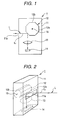
- An image input device 1 shown in Fig. 1 is designed so that a mirror body 12, a lens 13 and a linear sensor 14 are provided in a housing 11.
- the housing 11 is formed of a light shielding material. It is designed in a rectangular parallelepiped shape, for example, and is provided at one surface thereof with a slender incidence window 11a for passing image pickup light L from the subject therethrough into the inside of the housing 11. As described later, the incidence window 11 a is formed so that the length direction thereof is substantially parallel to the length direction of the mirror body 12.
- the mirror body 12 is designed in a polygonal prism form, and all the side peripheral surfaces 12a thereof are formed of mirror faces (hereinafter the side peripheral surface 12a is referred to as the mirror face 12a).
- the mirror body 12 is disposed in the housing 11 so that the length direction thereof is substantially parallel to the length direction of the linear sensor 14 and the image pickup light L from the incidence window 11a is reflected from the mirror face 12a.
- Figs. 1 and 2 show a case where the mirror body 12 has an octagonal prism form and each mirror face 12a is flat.
- the center of the plane which is substantially perpendicular to the length direction of the mirror body 12, that is, the substantial centers of the bottom surfaces 12b at both sides of the side peripheral surfaces 12a of the mirror body 12 are supported by a shaft 15 so as to be rotatable in the housing 11 and thus the mirror body 12 autorotates around the shaft 15. Furthermore, a first driving circuit (not shown) for rotating the mirror body 12 is connected to the mirror body 12.
- the lens 13 projects the image pickup light L onto the linear sensor 14.
- it is fixedly disposed between the mirror body 12 and the linear sensor 14 so as to project the image pickup light L reflected from the mirror face 12a of the mirror body 12 onto the linear sensor 14.
- the linear sensor 14 has a function of taking the image pickup light L reflected from the mirror body 12 to subject it to photoelectric conversion and outputting electrical signals thus obtained as video signals (image pickup information).
- a semiconductor image pickup device such as an MOS (metal oxide semiconductor) type sensor, a CCD (charge coupled device) type sensor or the like.
- a white-and-black sensor or a color sensor may be used as the linear sensor 14 using such a semiconductor image pickup device, and a coloring system using a combination of an external color filter and a white-and-black sensor may be used.
- a color sensor a 3-line color linear sensor, a dot-sequential type color linear sensor, a multi-line color linear sensor, a TDI type linear sensor or the like may be used.
- a peripheral circuit for driving the linear sensor 14, a signal processing circuit for performing signal processing of image pickup information output from the linear sensor 14, a timing signal generating circuit for outputting a timing signal to the first driving circuit of the mirror body 12 and the peripheral circuit of the linear sensor 14, etc., which are not shown in the figure, are provided in the housing 11 in which the mirror body 12, the lens and the linear sensor 14 are accommodated.
- the image pickup light L from the subject is incident from the incidence window 12 of the housing 11, reflected from the mirror surface 12a of the mirror body 12, passed through the lens 13 and then projected onto and taken into the linear sensor 14.
- the image pickup light L is taken into the linear sensor 14 so that the direction of the light component L 1 incident from the subject to the mirror face 12a is continuously varied because the arrangement positions of the mirror body 12, the lens 13 and the linear sensor 14 are fixed.
- the image pickup light obtained as if the linear sensor 14 scans the subject that is, the two-dimensional image information can be obtained.
- the linear sensor 14 since the linear sensor 14 may be arranged so as to take the image pickup light L projected onto the linear sensor 14, the image pickup information can be obtained with no effect even when the precision of the arrangement position of the linear sensor 14 is low as compared with the conventional linear scan camera. Therefore, the manufacturing work is very easy and thus the productivity can be enhanced.
- the housing 11 can be designed in a small size and image pickup information can be input in a short time.
- the power consumption can be more reduced.
- the positional relationship between the subject and the image input device 1 is not fixed, but some degree of freedom is provided to the distance therebetween, two-dimensional image information can be obtained by targeting a three-dimensional space as a subject.
- the positional relationship between the subject and the image input device 1 is not fixed and the housing 11 can be miniaturized, so that a portable image input device 1 can be designed.
- the mirror body 12 has a polygonal prism form, after image pickup light L reflected from a mirror face 12a is obtained, a subsequent adjacent mirror face 12a provides image pickup light L in which the direction of the light component L 1 incident to the mirror face 12A continuously varies as in the case of the previous face mirror 12a.
- a linear sensor 14 which can provide an image having a higher resolution as compared with an image input device using an area sensor, that is, a so-called digital camera. Accordingly, if the subject is still, the two-dimensional information of the same subject is repetitively taken into the linear sensor 14, so that a higher resolution still image can be obtained.
- a two-dimensional image having the same level image quality can be obtained at a still lower cost than a conventional digital camera using an area sensor which must be manufactured at a high cost because a large number of pixels are needed to obtain an ultra-high resolution image. Furthermore, if the image input device 1 is manufactured substantially at the same cost as the digital camera using the area sensor, a higher-resolution image can be obtained. If the subject has a motion, two-dimensional image information having continuous motions of the subject can be obtained. Therefore, the moving picture of the two-dimensional image can be obtained.
- the lens 13 is provided between the mirror body 12 and the linear sensor 14.
- the lens 13 may be provided between the incidence window 11a and the mirror body 12 so that the image pickup light L from the subject is incident to the mirror face 12a of the mirror body 12 through the lens 13.
- the mirror body is designed in an octagonal prism form.
- the shape of the mirror body is not limited to the above example.
- the mirror body is designed in a polygonal prism form under the condition that the intersecting angle between adjacent mirror faces is set to a predetermined value in consideration of functions such as optical correction, etc.
- each mirror face of the mirror body is flat.
- each mirror face may be curved in consideration of correction elements such as optical correction, etc. If the optical correction, etc. are carried out by using the shape of the mirror body, no correction circuit is needed to perform the optical correction, so that the image input device can be further miniaturized and the productivity can be further enhanced. Furthermore, when the optical correction, etc. can be performed on the basis of the intersecting angle between the adjacent mirror faces although each mirror face of the mirror body is flat, or when no optical correction is needed, the manufacturing cost of the mirror body can be reduced.
- FIG. 4A, 4B and Fig. 5 the same elements as the first embodiment are represented by the same reference numerals, and the description thereof is omitted.
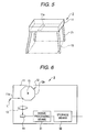
- the difference of the image input device 2 of the second example from the first example resides in that support legs 21 which are expandable from the housing 11 to the outside to support the housing 11 are provided on one surface of the housing 11 on which the incidence window 11a is formed.
- the support legs 21 are designed in a rod form, and they are provided at four comers on one surface of the housing 11 on which the incidence window 11a is formed, for example. Furthermore, as shown in Fig. 4A, they are provided so as to be retractable into the housing 11.
- Each of the four support legs 21 is designed to expand and contract.
- the support legs 21 are expanded from the housing 11, and the housing 11 is arranged through the support legs 21 on a table (not shown) so that the incidence window 11a of the housing 11 faces the subject 10 such as an original, a photograph or the like which is put on the table.
- the image pickup light L from the subject 10 is taken into the linear sensor 14 through the incidence window 11a, the mirror face 12a of the mirror body 12 and the lens 13 while the mirror body 12 in the housing 11 is rotated (see Fig. 1), or the image pickup light L is taken into the linear sensor 14 through the incidence window 11a, the lens 13 and the mirror face 12a of the mirror body 12 (see Fig. 3), and the image pickup light L thus taken is converted to a video signal, thereby obtaining image pickup information of the subject 10 such as an original, a photograph or the like. That is, the image input device functions as a so-called image scanner.
- the support legs 21 can be retracted into the housing 11, and they are put together in compact size, thereby facilitating portability of the device. Furthermore, the degree of freedom is provided to the distance between the subject and the image input device 1 by retracting the support legs 21 into the housing 11 as in the case of the image input device 1 of the first example, and thus two-dimensional image information can be obtained by targeting a three-dimensional space as a subject. Therefore, the image input device 2 of the second example has a function as a portable image scanner and a function of obtaining a two-dimensional still image or moving picture by targeting a three-dimensional space as a subject.
- the support legs are retractable into the housing, however, they may be detachably mounted to the housing.
- the rod-shaped support legs are respectively mounted at the four comers.
- any mounting manner may be used insofar as the support legs are provided to the housing so that the housing can be stably supported and the image input operation is not disturbed.
- three rod-shaped support legs may be provided, or two inverted T-shaped support legs are disposed so as to face each other.
- FIG. 6 the same elements as the first example of Figs. 1 and 2 are represented by the same reference numerals, and the description thereof is omitted.
- the difference of the image input device 3 of the third example from the first example resides in that storage means 32 for storing image pickup information output from the linear sensor 14 is provided in the housing 11 while it is connected to the linear sensor 14. Furthermore, in this example, signal processing means 31 comprising a signal processing circuit for subjecting the image pickup information from the linear sensor 14 to predetermined signal processing is provided between the linear sensor 14 and the storage means 32, and the image pickup information which is subjected to the signal processing in the signal processing means 31 is stored in the storage means 32.
- the storage means 32 is used a semiconductor memory such as RAM or the like, a floppy disk, MO (magnet optical) disk, a magnetic tape, a compact disk or the like.
- the image input device 3 as described above is provided with the storage means 32, and thus a large amount of image pickup information can be accumulated. Therefore, when two-dimensional moving pictures are obtained, the output from the linear sensor 14 can be accumulated in the storage means 32 every mirror face 12a of the mirror body 12 (every scan), and thus the image input device is very effective. Furthermore, the image pickup information thus accumulated is corrected on the time axis and output from the storage means 32 to a monitor to display two-dimensional moving pictures on the monitor. If the rotating timing of the mirror body 12 can be controlled so that it is unnecessary to correct the time axis for the image pickup information output from the linear sensor 14 when moving pictures are obtained, the storage means 32 may be omitted.
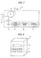
- FIG. 7 A fourth example of an image input device will be described with reference to Fig. 7.
- the same elements as the third example are represented by the same reference numerals, and the description thereof is omitted.
- the difference of the image input device 4 of the fourth example from the third example resides in that an external interface 41 serving as communication means to communicate the image pickup information output from the linear sensor 14 to the outside is provided in the housing 11 so as to be connected to the linear sensor 14.
- the image pickup information from the linear sensor 14 is input to the external interface 41 through the signal processing means 31 and the storage means 32.
- the external interface 41 may be used a communication circuit having RS232, 1349, USB, IRDA and a portable telephone function, an originally-standardized interactive or unidirectional communication circuit or the like.
- the image input device 4 described above is provided with the external interface 41, and thus the image pickup information accumulated in the storage means 32 can be transmitted through the external interface 41 to the outside. Therefore, the image pickup information can be transferred from the storage means 32 through the external interface 41 to another storage medium or the like, so that the storage means 32 is allowed to store a large amount of information at all times. Furthermore, even at a remote place, an image input from the image input device 4 can be transmitted and viewed.
- the image input devices 1 to 4 of the above first to fourth examples may be provided with optical or electrical hand-movement correcting means for correcting the movement of hands.
- the optical hand-movement correcting means comprises a lens portion containing a lens 13 and an active prism installed in the lens 13, and a hand-movement detector.
- the hand-movement is corrected by varying the refraction of the image pickup light L through the lens portion in accordance with the detection of the hand-movement in the hand-movement detector.
- the electrical hand-movement correcting means comprises a linear sensor 14 having a broader image pickup area than the effective angle of view corresponding to the image pickup information, and a hand-movement detector. The effective angle of view is moved in accordance with the detection of the movement of hands to correct the movement of hands.
- FIG. 8 the same elements as the first example are represented by the same reference numerals, and the description thereof is omitted.
- the difference of the image input device 5 of this embodiment resides in that a plurality of illuminators 51 which are successively turned on to light up to the subject are provided in the housing 11.
- a number of illuminators 51 are arranged on one surface of the housing 11 on which the incidence window 11a is provided.
- each illuminator 51 comprises an electronic flash such as a xenon lamp or the like.
- a second driving circuit 52 serving as second driving means for successively turning on the illuminators 51 is provided in the housing 11.
- a first driving circuit 16 serving as first driving means for rotating the mirror body 12, a peripheral circuit 17 for driving the linear sensor 14, a second driving circuit 52 and a timing signal generating circuit (timing signal generating means) 53 for outputting timing signals to the first driving circuit 16, the peripheral circuit 17 and the second driving circuit 52 are provided in the housing 11.
- the timing signal generating circuit 53 outputs the timing signals to the first driving circuit 16 and the second driving circuit 17 so that the illuminators 51 are turned on at a predetermined timing with respect to the rotation of the mirror body 12.
- the first driving circuit 16 and the second driving circuit 17 serve to rotate the mirror body 12 and turn on the illuminators 51.
- the timing signal generating circuit 53 is supplied with a vertical synchronous signal (hereinafter referred to as VD signal).
- VD signal a vertical synchronous signal
- the timing signal generating circuit 53 outputs to the second driving circuit 52 a trigger pulse which is a timing signal for turning on the illuminators 51 in synchronism with the VD signal.
- the timing signal generating circuit 53 has a function of outputting to the first driving circuit 16 a timing signal for rotating the mirror body 12 in ) synchronism with the VD signal.
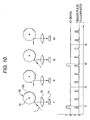
- Fig. 10 is a timing chart showing an example of the timing relationship between the VD signal and the trigger pulse output to the second driving circuit 52.
- the trigger pulse is output from the timing signal generating circuit 53 to the second driving circuit 52 substantially simultaneously with input of the VD signal to the timing signal generating circuit 53.
- the timing signal is output to the first driving circuit 16 so that the mirror body 12 is rotated at such a speed that the reflection of the image pickup light L is started and ended at one mirror face 12a of the mirror body 12, that is, one scan operation is completed during the time period from input of a VD signal until input of a next VD signal. Furthermore, representing the start time point of the reflection of the image pickup light L at a mirror face 12a by t 1 and representing the start time point of the image pickup light L at an adjacent mirror face 12a by t 3 , a trigger pulse is output to the second driving circuit 52 at an equal interval, for example at five times between t 1 and t 3 to successively turn on the illuminators 51.
- a plurality of illuminators 51 which are successively turned on to light up to the subject are provided in the housing 11, and the illuminators 51 can be successively turned on when image pickup light L (of one scan) reflected from a mirror face is obtained.
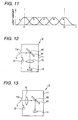
- the light amount of each of the illuminators 51 a to e varies like a Gaussian distribution as shown in Fig. 11, but the sum of the light amount can be set to a substantially fixed value by successively turning on the illuminators during one scan period (the sum is indicated by one-dotted chain line in Fig. 11).
- light can be substantially uniformly irradiated to the subject during one scan period.
- the accumulation time of the image pickup light L to be taken per scan is shorter as compared with the area sensor, the image pickup light L having a large accumulation amount can be obtained. Therefore, information of a clear and uniform two-dimensional image can be obtained under such an environment that a subject serving as a target is short of light amount, for example, under a dark three-dimensional space such as night or the like.
- the illuminators, the first driving means, the second driving means, the timing signal generating means, etc. are installed into the image input device 1 of the first example, thereby constructing the image input device 5.
- the illuminators, etc. may be installed into the image input device 1 of the modification shown in Fig. 3, the image input device 2 of the second example, the image input device 3 of the third example or the image input device 4 of the fourth example, thereby constructing the image input device which can provide clear and uniform two-dimensional image information even under a three-dimensional space which lacks light amount.
- the illuminators 51, etc. may be installed to an image input device 6 having a flat-plate type mirror body 61 as shown in a first modification of Fig. 12 and a second modification of Fig. 13.
- This mirror body 61 is formed of mirror face on one surface or both the surfaces thereof, and a shaft 62 is formed along the mirror face within the thickness of the mirror body 61.
- the mirror body 61 is supported by the shaft 62, and rotatable or swingable around the shaft 62.
- the incidence window 11a is formed so that the length direction thereof is substantially parallel to the shaft 62 of the mirror body 61. It is needless to say that clear and uniform two-dimensional image information can be obtained by even such an image input device 6.
- plural illuminators which are successively turned on to light up to the subject are provided in the housing in which the mirror body and the linear sensor are accommodated, and when image pickup light (of one scan) reflected from a mirror face is obtained, the illuminators are successively turned on to irradiate uniform light to the subject. Therefore, clear and uniform two-dimensional image information can be obtained even under such an environment that a target subject lacks light amount, for example, under a dark three-dimensional space such as night or the like.
Description
- The present invention relates to an image input device to obtain a three-dimensional image by using a linear sensor.
- The following two types of image input devices have been hitherto generally known as an image input device to obtain a two-dimensional image by using a linear sensor. One type is an image scanner which is being remarkably popular at present. The other type is a device in which a linear sensor is disposed on a film face of a silver chloride camera using middle-size or large-size films and then the linear sensor is moved along the film face to obtain a two-dimensional image (hereinafter referred to as "linear sensor scan camera"). As compared with an image input device for obtaining a two-dimensional image by using an area sensor, both the above devices have an advantage that a two-dimensional image of ultra-high resolution can be obtained.
- However, in the conventional image input devices, in the case of the former image scanner, the positional relationship between a subject and an image scanner is substantially fixed, and thus there is no degree of freedom in distance between the subject and the image scanner. Furthermore, in the case of the latter linear sensor scanner camera, the severe mechanical precision is required to move the linear sensor, so that it needs much time and effort to manufacture a precise moving mechanism and the cost is increased. In addition, since the speed at which the linear sensor is moved is low, there is such a drawback that it takes much time to input a two-dimensional image.
- Accordingly, in any system described above, at present it is difficult to convert a three-dimensional space to a two-dimensional image by using a linear sensor. From such a situation, it is practically difficult to obtain a two-dimensional moving picture by using a linear sensor.
- Furthermore, since the linear sensor is designed like a line, the accumulation time of image pickup information of one scan is shorter than that of the area sensor. As a result, even when the subject is exposed to the same light, an image obtained is darker as compared with an image input device using a linear sensor. Accordingly, from this viewpoint, it is difficult to convert the three-dimensional space to the two-dimensional image under such an environment as night or rainy situation which lacks light amount.
- US5625183 A describes a scanning image input device according to the preamble of
claim 1. JP 1093258 A describes an image input device with a plurality of successively activated light sources. - The scanning image input device of the present invention is as described in the apended claims.
-
- Fig. 1 is a diagram showing the construction of a first example of an image input device;
- Fig. 2 is a perspective view showing the first example of an image input device;
- Fig. 3 is a diagram showing the construction of a modification of the first example;
- Figs. 4A and 4B are front views showing a second example of an image input device, wherein Fig. 4A shows a state where support legs are retracted in a housing, and Fig. 4B shows a state where the support legs are expanded;
- Fig. 5 is a perspective view showing the second example of an image input device;
- Fig. 6 is a diagram showing the construction of a third example of an image input device;
- Fig. 7 is a diagram showing the construction of a fourth example of an image input device;
- Fig. 8 is a perspective view showing an embodiment of the image input device according to the present invention;
- Fig. 9 is a diagram showing the construction of the embodiment of the image input device according to the present invention;
- Fig. 10 is a timing chart showing an example of the timing relationship between a VD signal and a trigger pulse for turning on illuminators;
- Fig. 11 is a diagram showing an example of a light amount distribution during one scan;
- Fig. 12 is a diagram showing a first modification of the embodiment; and
- Fig. 13 is a diagram showing a second modification of the embodiment.
-
- Examples of image input devices and preferred embodiments of an image input device according to the present invention will be described with reference to the accompanying drawings.
- Fig. 1 is a schematic diagram showing the construction of a first example of an image input device, and Fig. 2 is a perspective view showing the first example of an image input device.
- An
image input device 1 shown in Fig. 1 is designed so that amirror body 12, alens 13 and alinear sensor 14 are provided in ahousing 11. Thehousing 11 is formed of a light shielding material. It is designed in a rectangular parallelepiped shape, for example, and is provided at one surface thereof with aslender incidence window 11a for passing image pickup light L from the subject therethrough into the inside of thehousing 11. As described later, theincidence window 11 a is formed so that the length direction thereof is substantially parallel to the length direction of themirror body 12. - The
mirror body 12 is designed in a polygonal prism form, and all the sideperipheral surfaces 12a thereof are formed of mirror faces (hereinafter the sideperipheral surface 12a is referred to as themirror face 12a). Themirror body 12 is disposed in thehousing 11 so that the length direction thereof is substantially parallel to the length direction of thelinear sensor 14 and the image pickup light L from theincidence window 11a is reflected from themirror face 12a. Figs. 1 and 2 show a case where themirror body 12 has an octagonal prism form and eachmirror face 12a is flat. - The center of the plane which is substantially perpendicular to the length direction of the
mirror body 12, that is, the substantial centers of thebottom surfaces 12b at both sides of the sideperipheral surfaces 12a of themirror body 12 are supported by ashaft 15 so as to be rotatable in thehousing 11 and thus themirror body 12 autorotates around theshaft 15. Furthermore, a first driving circuit (not shown) for rotating themirror body 12 is connected to themirror body 12. - The
lens 13 projects the image pickup light L onto thelinear sensor 14. In this example, it is fixedly disposed between themirror body 12 and thelinear sensor 14 so as to project the image pickup light L reflected from themirror face 12a of themirror body 12 onto thelinear sensor 14. - The
linear sensor 14 has a function of taking the image pickup light L reflected from themirror body 12 to subject it to photoelectric conversion and outputting electrical signals thus obtained as video signals (image pickup information). As thelinear sensor 14 may be used a semiconductor image pickup device such as an MOS (metal oxide semiconductor) type sensor, a CCD (charge coupled device) type sensor or the like. - A white-and-black sensor or a color sensor may be used as the
linear sensor 14 using such a semiconductor image pickup device, and a coloring system using a combination of an external color filter and a white-and-black sensor may be used. As the color sensor, a 3-line color linear sensor, a dot-sequential type color linear sensor, a multi-line color linear sensor, a TDI type linear sensor or the like may be used. - Furthermore, a peripheral circuit for driving the
linear sensor 14, a signal processing circuit for performing signal processing of image pickup information output from thelinear sensor 14, a timing signal generating circuit for outputting a timing signal to the first driving circuit of themirror body 12 and the peripheral circuit of thelinear sensor 14, etc., which are not shown in the figure, are provided in thehousing 11 in which themirror body 12, the lens and thelinear sensor 14 are accommodated. - In the
image input device 1 thus constructed, the image pickup light L from the subject is incident from theincidence window 12 of thehousing 11, reflected from themirror surface 12a of themirror body 12, passed through thelens 13 and then projected onto and taken into thelinear sensor 14. At this time, when themirror body 12 is rotated, the image pickup light L is taken into thelinear sensor 14 so that the direction of the light component L1 incident from the subject to themirror face 12a is continuously varied because the arrangement positions of themirror body 12, thelens 13 and thelinear sensor 14 are fixed. As a result, the image pickup light obtained as if thelinear sensor 14 scans the subject, that is, the two-dimensional image information can be obtained. - Accordingly, it is unnecessary to provide a precise moving mechanism for moving the
linear sensor 14 like a conventional linear scan camera, and thus a two-dimensional image can be obtained at a low cost as compared with the conventional linear scan camera. Furthermore, in theimage input 1 device of the first example, since thelinear sensor 14 may be arranged so as to take the image pickup light L projected onto thelinear sensor 14, the image pickup information can be obtained with no effect even when the precision of the arrangement position of thelinear sensor 14 is low as compared with the conventional linear scan camera. Therefore, the manufacturing work is very easy and thus the productivity can be enhanced. - Furthermore, since it is unnecessary to move the
linear sensor 14 and themirror body 12 is merely autorotated, thehousing 11 can be designed in a small size and image pickup information can be input in a short time. In addition, as compared with the conventional linear scan camera which moves thelinear sensor 14, the power consumption can be more reduced. Furthermore, since the positional relationship between the subject and theimage input device 1 is not fixed, but some degree of freedom is provided to the distance therebetween, two-dimensional image information can be obtained by targeting a three-dimensional space as a subject. The positional relationship between the subject and theimage input device 1 is not fixed and thehousing 11 can be miniaturized, so that a portableimage input device 1 can be designed. - Still further, since the
mirror body 12 has a polygonal prism form, after image pickup light L reflected from amirror face 12a is obtained, a subsequentadjacent mirror face 12a provides image pickup light L in which the direction of the light component L1 incident to the mirror face 12A continuously varies as in the case of theprevious face mirror 12a. In addition, there is used alinear sensor 14 which can provide an image having a higher resolution as compared with an image input device using an area sensor, that is, a so-called digital camera. Accordingly, if the subject is still, the two-dimensional information of the same subject is repetitively taken into thelinear sensor 14, so that a higher resolution still image can be obtained. - Therefore, a two-dimensional image having the same level image quality can be obtained at a still lower cost than a conventional digital camera using an area sensor which must be manufactured at a high cost because a large number of pixels are needed to obtain an ultra-high resolution image. Furthermore, if the
image input device 1 is manufactured substantially at the same cost as the digital camera using the area sensor, a higher-resolution image can be obtained. If the subject has a motion, two-dimensional image information having continuous motions of the subject can be obtained. Therefore, the moving picture of the two-dimensional image can be obtained. - In the above first example, the
lens 13 is provided between themirror body 12 and thelinear sensor 14. However, as a modification shown in Fig. 3, thelens 13 may be provided between theincidence window 11a and themirror body 12 so that the image pickup light L from the subject is incident to themirror face 12a of themirror body 12 through thelens 13. - In the above first example, the mirror body is designed in an octagonal prism form. However, the shape of the mirror body is not limited to the above example. For example, the mirror body is designed in a polygonal prism form under the condition that the intersecting angle between adjacent mirror faces is set to a predetermined value in consideration of functions such as optical correction, etc.
- Furthermore, in the foregoing description, each mirror face of the mirror body is flat. However, each mirror face may be curved in consideration of correction elements such as optical correction, etc. If the optical correction, etc. are carried out by using the shape of the mirror body, no correction circuit is needed to perform the optical correction, so that the image input device can be further miniaturized and the productivity can be further enhanced. Furthermore, when the optical correction, etc. can be performed on the basis of the intersecting angle between the adjacent mirror faces although each mirror face of the mirror body is flat, or when no optical correction is needed, the manufacturing cost of the mirror body can be reduced.
- Next, a second example of an image input device will be described with reference to Figs. 4A, 4B and Fig. 5. In Figs. 4A, 4B and 5, the same elements as the first embodiment are represented by the same reference numerals, and the description thereof is omitted.
- The difference of the
image input device 2 of the second example from the first example resides in thatsupport legs 21 which are expandable from thehousing 11 to the outside to support thehousing 11 are provided on one surface of thehousing 11 on which theincidence window 11a is formed. In the second example, thesupport legs 21 are designed in a rod form, and they are provided at four comers on one surface of thehousing 11 on which theincidence window 11a is formed, for example. Furthermore, as shown in Fig. 4A, they are provided so as to be retractable into thehousing 11. Each of the foursupport legs 21 is designed to expand and contract. - In the
image input device 2 described above, as shown in Fig. 5, thesupport legs 21 are expanded from thehousing 11, and thehousing 11 is arranged through thesupport legs 21 on a table (not shown) so that theincidence window 11a of thehousing 11 faces the subject 10 such as an original, a photograph or the like which is put on the table. - Accordingly, as in the case of the first example, the image pickup light L from the subject 10 is taken into the
linear sensor 14 through theincidence window 11a, themirror face 12a of themirror body 12 and thelens 13 while themirror body 12 in thehousing 11 is rotated (see Fig. 1), or the image pickup light L is taken into thelinear sensor 14 through theincidence window 11a, thelens 13 and themirror face 12a of the mirror body 12 (see Fig. 3), and the image pickup light L thus taken is converted to a video signal, thereby obtaining image pickup information of the subject 10 such as an original, a photograph or the like. That is, the image input device functions as a so-called image scanner. - Furthermore, after the image input operation, the
support legs 21 can be retracted into thehousing 11, and they are put together in compact size, thereby facilitating portability of the device. Furthermore, the degree of freedom is provided to the distance between the subject and theimage input device 1 by retracting thesupport legs 21 into thehousing 11 as in the case of theimage input device 1 of the first example, and thus two-dimensional image information can be obtained by targeting a three-dimensional space as a subject. Therefore, theimage input device 2 of the second example has a function as a portable image scanner and a function of obtaining a two-dimensional still image or moving picture by targeting a three-dimensional space as a subject. - In the second example, the support legs are retractable into the housing, however, they may be detachably mounted to the housing. Furthermore, the rod-shaped support legs are respectively mounted at the four comers. However, any mounting manner may be used insofar as the support legs are provided to the housing so that the housing can be stably supported and the image input operation is not disturbed. For example, three rod-shaped support legs may be provided, or two inverted T-shaped support legs are disposed so as to face each other.
- Next, a third example of an image input device will be described with reference to Fig. 6. In Fig. 6, the same elements as the first example of Figs. 1 and 2 are represented by the same reference numerals, and the description thereof is omitted.
- The difference of the
image input device 3 of the third example from the first example resides in that storage means 32 for storing image pickup information output from thelinear sensor 14 is provided in thehousing 11 while it is connected to thelinear sensor 14. Furthermore, in this example, signal processing means 31 comprising a signal processing circuit for subjecting the image pickup information from thelinear sensor 14 to predetermined signal processing is provided between thelinear sensor 14 and the storage means 32, and the image pickup information which is subjected to the signal processing in the signal processing means 31 is stored in the storage means 32. As the storage means 32 is used a semiconductor memory such as RAM or the like, a floppy disk, MO (magnet optical) disk, a magnetic tape, a compact disk or the like. - The
image input device 3 as described above is provided with the storage means 32, and thus a large amount of image pickup information can be accumulated. Therefore, when two-dimensional moving pictures are obtained, the output from thelinear sensor 14 can be accumulated in the storage means 32 everymirror face 12a of the mirror body 12 (every scan), and thus the image input device is very effective. Furthermore, the image pickup information thus accumulated is corrected on the time axis and output from the storage means 32 to a monitor to display two-dimensional moving pictures on the monitor. If the rotating timing of themirror body 12 can be controlled so that it is unnecessary to correct the time axis for the image pickup information output from thelinear sensor 14 when moving pictures are obtained, the storage means 32 may be omitted. - A fourth example of an image input device will be described with reference to Fig. 7. In Fig. 7, the same elements as the third example are represented by the same reference numerals, and the description thereof is omitted.
- The difference of the image input device 4 of the fourth example from the third example resides in that an
external interface 41 serving as communication means to communicate the image pickup information output from thelinear sensor 14 to the outside is provided in thehousing 11 so as to be connected to thelinear sensor 14. In this example, the image pickup information from thelinear sensor 14 is input to theexternal interface 41 through the signal processing means 31 and the storage means 32. As theexternal interface 41 may be used a communication circuit having RS232, 1349, USB, IRDA and a portable telephone function, an originally-standardized interactive or unidirectional communication circuit or the like. - The image input device 4 described above is provided with the
external interface 41, and thus the image pickup information accumulated in the storage means 32 can be transmitted through theexternal interface 41 to the outside. Therefore, the image pickup information can be transferred from the storage means 32 through theexternal interface 41 to another storage medium or the like, so that the storage means 32 is allowed to store a large amount of information at all times. Furthermore, even at a remote place, an image input from the image input device 4 can be transmitted and viewed. - The
image input devices 1 to 4 of the above first to fourth examples may be provided with optical or electrical hand-movement correcting means for correcting the movement of hands. The optical hand-movement correcting means comprises a lens portion containing alens 13 and an active prism installed in thelens 13, and a hand-movement detector. In the hand-movement correcting means thus constructed, the hand-movement is corrected by varying the refraction of the image pickup light L through the lens portion in accordance with the detection of the hand-movement in the hand-movement detector. The electrical hand-movement correcting means comprises alinear sensor 14 having a broader image pickup area than the effective angle of view corresponding to the image pickup information, and a hand-movement detector. The effective angle of view is moved in accordance with the detection of the movement of hands to correct the movement of hands. - Next, an embodiment of the image input device according to the present invention will be described with reference to the perspective view of Fig. 8 and the schematic diagram of Fig. 9. In Figs. 8 and 9, the same elements as the first example are represented by the same reference numerals, and the description thereof is omitted.
- The difference of the
image input device 5 of this embodiment resides in that a plurality ofilluminators 51 which are successively turned on to light up to the subject are provided in thehousing 11. In Fig. 7, a number ofilluminators 51 are arranged on one surface of thehousing 11 on which theincidence window 11a is provided. However, if illuminators can be alternatively turned on at high speed, only twoilluminators 51 may be provided. Furthermore, each illuminator 51 comprises an electronic flash such as a xenon lamp or the like. - A
second driving circuit 52 serving as second driving means for successively turning on theilluminators 51 is provided in thehousing 11. In addition, afirst driving circuit 16 serving as first driving means for rotating themirror body 12, aperipheral circuit 17 for driving thelinear sensor 14, asecond driving circuit 52 and a timing signal generating circuit (timing signal generating means) 53 for outputting timing signals to thefirst driving circuit 16, theperipheral circuit 17 and thesecond driving circuit 52 are provided in thehousing 11. - The timing
signal generating circuit 53 outputs the timing signals to thefirst driving circuit 16 and thesecond driving circuit 17 so that theilluminators 51 are turned on at a predetermined timing with respect to the rotation of themirror body 12. In accordance with the timing signals, thefirst driving circuit 16 and thesecond driving circuit 17 serve to rotate themirror body 12 and turn on theilluminators 51. - For example, the timing
signal generating circuit 53 is supplied with a vertical synchronous signal (hereinafter referred to as VD signal). The timingsignal generating circuit 53 outputs to the second driving circuit 52 a trigger pulse which is a timing signal for turning on theilluminators 51 in synchronism with the VD signal. The timingsignal generating circuit 53 has a function of outputting to the first driving circuit 16 a timing signal for rotating themirror body 12 in ) synchronism with the VD signal. - Fig. 10 is a timing chart showing an example of the timing relationship between the VD signal and the trigger pulse output to the
second driving circuit 52. In this case, the trigger pulse is output from the timingsignal generating circuit 53 to thesecond driving circuit 52 substantially simultaneously with input of the VD signal to the timingsignal generating circuit 53. - The timing signal is output to the
first driving circuit 16 so that themirror body 12 is rotated at such a speed that the reflection of the image pickup light L is started and ended at onemirror face 12a of themirror body 12, that is, one scan operation is completed during the time period from input of a VD signal until input of a next VD signal. Furthermore, representing the start time point of the reflection of the image pickup light L at amirror face 12a by t1 and representing the start time point of the image pickup light L at anadjacent mirror face 12a by t3, a trigger pulse is output to thesecond driving circuit 52 at an equal interval, for example at five times between t1 and t3 to successively turn on theilluminators 51. - As described above, in the
image input device 5 of this embodiment, a plurality ofilluminators 51 which are successively turned on to light up to the subject are provided in thehousing 11, and theilluminators 51 can be successively turned on when image pickup light L (of one scan) reflected from a mirror face is obtained. Representing a line of laterally-arrangedilluminators 51 shown in Fig. 8 by a, b, c, d, e, the light amount of each of the illuminators 51 a to e varies like a Gaussian distribution as shown in Fig. 11, but the sum of the light amount can be set to a substantially fixed value by successively turning on the illuminators during one scan period (the sum is indicated by one-dotted chain line in Fig. 11). As a result, light can be substantially uniformly irradiated to the subject during one scan period. - Accordingly, although in the
linear sensor 14 the accumulation time of the image pickup light L to be taken per scan is shorter as compared with the area sensor, the image pickup light L having a large accumulation amount can be obtained. Therefore, information of a clear and uniform two-dimensional image can be obtained under such an environment that a subject serving as a target is short of light amount, for example, under a dark three-dimensional space such as night or the like. - In this embodiment, the illuminators, the first driving means, the second driving means, the timing signal generating means, etc. according to the present invention are installed into the
image input device 1 of the first example, thereby constructing theimage input device 5. However, it is needless to say that the illuminators, etc. may be installed into theimage input device 1 of the modification shown in Fig. 3, theimage input device 2 of the second example, theimage input device 3 of the third example or the image input device 4 of the fourth example, thereby constructing the image input device which can provide clear and uniform two-dimensional image information even under a three-dimensional space which lacks light amount. - Furthermore, in place of using the mirror body having the polygonal prism form, the
illuminators 51, etc. may be installed to animage input device 6 having a flat-platetype mirror body 61 as shown in a first modification of Fig. 12 and a second modification of Fig. 13. Thismirror body 61 is formed of mirror face on one surface or both the surfaces thereof, and ashaft 62 is formed along the mirror face within the thickness of themirror body 61. Themirror body 61 is supported by theshaft 62, and rotatable or swingable around theshaft 62. Theincidence window 11a is formed so that the length direction thereof is substantially parallel to theshaft 62 of themirror body 61. It is needless to say that clear and uniform two-dimensional image information can be obtained by even such animage input device 6. - As described above, according to the image input device of the present invention, plural illuminators which are successively turned on to light up to the subject are provided in the housing in which the mirror body and the linear sensor are accommodated, and when image pickup light (of one scan) reflected from a mirror face is obtained, the illuminators are successively turned on to irradiate uniform light to the subject. Therefore, clear and uniform two-dimensional image information can be obtained even under such an environment that a target subject lacks light amount, for example, under a dark three-dimensional space such as night or the like.
Claims (8)
- A scanning image input device comprising:a housing (11) having a slender incidence window (11a) to pass image pickup light from a subject therethrough into said housing (11);a mirror body (12) rotatably or swingably provided in said housing (11), having mirror faces (12a) for reflecting the image pickup light from said incident window (11a); anda linear sensor (14) which is disposed in said housing (11) and takes the image pickup light reflected from said mirror body (12) to subject the image pickup light to photoelectric conversion; and characterised in that said image input device further comprises:a plurality of electronic flash illuminators (51) which are provided in said housing (11) and means for successively turning on said electronic flash illuminators to irradiate the subject substantially uniformly during one scan period.
- The image input device as claimed in claim 1, wherein said mirror body (12) is designed in a polygonal prism form and formed of said mirror faces (12a) on all the side peripheral surfaces thereof, and disposed so that the length direction thereof is substantially parallel to the length direction of said linear sensor (14) and provided so as to be rotatable around the center (15) of the plane which is substantially perpendicular to the length direction of said mirror body (12), and wherein said incidence window (11a) is formed so that the length direction thereof is substantially parallel to the length direction of said mirror body (12).
- The image input device as claimed in claim 1, wherein said mirror body (12) is designed in the form of a flat plate, one face or both faces thereof being formed of said mirror faces (12a), and a shaft (15) is formed along said mirror faces (12a) so as to be located within said mirror body (12) so that said mirror body (12) is rotatable or swingable around said shaft (15), and wherein said incidence window (11a) is formed so that the length direction is substantially parallel to said shaft (15) of said mirror body (12).
- The image input device as claimed in claim 1, further including:first driving means (16) for rotating or swinging said mirror body (12);second driving means (52) for successively turning on said plural illuminators (51); andtiming signal generating means (53) for outputting timing signals to said first driving means (16) and said second driving means (52) so that said illuminators (51) are successively turned on at a predetermined timing with respect to the rotational or swinging motion of said mirror body (12).
- The image input device as claimed in claim 1, further including support legs (21) which are formed at the formation side of said incidence window (11a) of said housing (11) so as to expand from said housing (11) to the outside and support said housing (11), said support legs (21) being provided so as to be retractable into said housing (11) or detachably mounted to said housing (11).
- The image input device as claimed in claim 1, further including storage means (32) for storing image pickup information output from said linear sensor (14).
- The image input device as claimed in claim 1, further including communication means (41) for communicating image pickup information output from said linear sensor (14) to the outside.
- The image input device as claimed in claim 1, wherein said linear sensor (14) is constructed by a semiconductor image pickup element.
Applications Claiming Priority (3)
| Application Number | Priority Date | Filing Date | Title |
|---|---|---|---|
| JP10091078A JPH11289495A (en) | 1998-04-03 | 1998-04-03 | Image input device |
| JP9107898 | 1998-04-03 | ||
| EP99400818A EP0948196B1 (en) | 1998-04-03 | 1999-04-02 | Image input device |
Related Parent Applications (1)
| Application Number | Title | Priority Date | Filing Date |
|---|---|---|---|
| EP99400818A Division EP0948196B1 (en) | 1998-04-03 | 1999-04-02 | Image input device |
Publications (2)
| Publication Number | Publication Date |
|---|---|
| EP1255151A1 EP1255151A1 (en) | 2002-11-06 |
| EP1255151B1 true EP1255151B1 (en) | 2004-06-16 |
Family
ID=14016485
Family Applications (2)
| Application Number | Title | Priority Date | Filing Date |
|---|---|---|---|
| EP99400818A Expired - Lifetime EP0948196B1 (en) | 1998-04-03 | 1999-04-02 | Image input device |
| EP02077920A Expired - Lifetime EP1255151B1 (en) | 1998-04-03 | 1999-04-02 | Image input device |
Family Applications Before (1)
| Application Number | Title | Priority Date | Filing Date |
|---|---|---|---|
| EP99400818A Expired - Lifetime EP0948196B1 (en) | 1998-04-03 | 1999-04-02 | Image input device |
Country Status (6)
| Country | Link |
|---|---|
| US (1) | US6917385B1 (en) |
| EP (2) | EP0948196B1 (en) |
| JP (1) | JPH11289495A (en) |
| CN (1) | CN1183478C (en) |
| DE (2) | DE69918190T2 (en) |
| TW (1) | TW420944B (en) |
Families Citing this family (9)
| Publication number | Priority date | Publication date | Assignee | Title |
|---|---|---|---|---|
| TWI231050B (en) * | 2003-09-29 | 2005-04-11 | Primax Electronics Ltd | Moveable mirror module for an image capturing apparatus capable of taking multi angle pictures |
| FR2867645A1 (en) * | 2004-03-15 | 2005-09-16 | Jean Rene Eude | Two or three dimensional digital image creating device for digital camera, has electron optics to produce transversal scanning lines that are stored in memory, and sequencer to place each line successively to restore image on digital screen |
| US7567287B2 (en) * | 2006-09-20 | 2009-07-28 | Sony Ericsson Mobile Communications Ab | Rotating prism for a digital camera in a portable mobile communication device |
| JP4653123B2 (en) * | 2007-01-09 | 2011-03-16 | 富士フイルム株式会社 | Image acquisition apparatus and image acquisition method |
| CN102045481B (en) * | 2009-10-10 | 2013-03-20 | 上海祥网瑞电子科技有限公司 | Rapid planar image collector with switching lens |
| US20150169046A1 (en) * | 2013-12-13 | 2015-06-18 | Honeywell International Inc. | Line scan camera eye tracking system and method |
| DE102015215840B4 (en) * | 2015-08-19 | 2017-03-23 | Fraunhofer-Gesellschaft zur Förderung der angewandten Forschung e.V. | A multi-aperture imaging apparatus, imaging system, and method of providing a multi-aperture imaging apparatus |
| WO2017156302A1 (en) * | 2016-03-10 | 2017-09-14 | Visbit Inc. | Time multiplexing programmable field of view imaging |
| JPWO2020066402A1 (en) * | 2018-09-25 | 2021-08-30 | 株式会社小糸製作所 | Light irradiation device |
Family Cites Families (23)
| Publication number | Priority date | Publication date | Assignee | Title |
|---|---|---|---|---|
| US3137532A (en) * | 1962-08-29 | 1964-06-16 | Tyll Charles | Instrument cases |
| JPS6337772A (en) | 1986-08-01 | 1988-02-18 | Nec Home Electronics Ltd | Image input device |
| JPH0193258A (en) | 1987-10-05 | 1989-04-12 | Casio Comput Co Ltd | Image reader |
| JPH04203915A (en) | 1990-11-30 | 1992-07-24 | Hitachi Ltd | Method and apparatus for inputting image of large visual field |
| CA2065482A1 (en) * | 1991-04-11 | 1992-10-12 | Akira Inoue | Method and apparatus for measuring a coating state |
| JPH06197250A (en) | 1992-02-21 | 1994-07-15 | Hitachi Ltd | Video camera |
| US5748236A (en) * | 1993-12-10 | 1998-05-05 | Nikon Corporation | Color mixing prevention and color balance setting device and method for a field-sequential color television camera |
| US5668631A (en) * | 1993-12-20 | 1997-09-16 | Minolta Co., Ltd. | Measuring system with improved method of reading image data of an object |
| US5671080A (en) * | 1993-12-22 | 1997-09-23 | Olympus Optical Co., Ltd. | Optical system scanning with a mirror for electronic image pickup apparatus |
| US5625183A (en) | 1994-06-15 | 1997-04-29 | Nec Corporation | Rotary mirror scanner unit having optical angular displacement sensor |
| DE4428202A1 (en) * | 1994-08-09 | 1996-02-15 | Deutsche Forsch Luft Raumfahrt | Device for generating an image |
| JPH0870407A (en) | 1994-08-26 | 1996-03-12 | Toshiba Corp | Image pickup device |
| JPH08274956A (en) * | 1995-03-30 | 1996-10-18 | Nec Corp | Image scanner |
| JPH09307676A (en) * | 1996-03-14 | 1997-11-28 | Nikon Corp | Image reader |
| JP3397580B2 (en) * | 1996-06-07 | 2003-04-14 | ペンタックス株式会社 | Remotely controllable scanner |
| US5993077A (en) * | 1996-08-05 | 1999-11-30 | Jones; Steven P. | Stand assembly for an optical device |
| US6426776B1 (en) * | 1997-03-18 | 2002-07-30 | Minolta Co., Ltd. | Apparatus for and method of photographing using scanning techniques |
| JPH10290321A (en) * | 1997-04-14 | 1998-10-27 | Nikon Corp | Image reader and transmission original adapter |
| JPH11243471A (en) * | 1998-02-26 | 1999-09-07 | Brother Ind Ltd | Color reader and storage medium |
| US6462772B1 (en) * | 1998-12-23 | 2002-10-08 | Eastman Kodak Company | Method of calibrating image scanning apparatus of a photographic film scanner |
| US20030183746A1 (en) * | 2002-04-02 | 2003-10-02 | Pao-Jung Chen | High speed single-linear three-color CIS image sensing array |
| KR100449729B1 (en) * | 2002-06-29 | 2004-09-22 | 삼성전자주식회사 | Optical scanning apparatus |
| JP2004109204A (en) * | 2002-09-13 | 2004-04-08 | Pentax Corp | Scanning optical system |
-
1998
- 1998-04-03 JP JP10091078A patent/JPH11289495A/en active Pending
-
1999
- 1999-04-01 TW TW088105198A patent/TW420944B/en not_active IP Right Cessation
- 1999-04-01 US US09/283,233 patent/US6917385B1/en not_active Expired - Fee Related
- 1999-04-01 CN CNB991059182A patent/CN1183478C/en not_active Expired - Fee Related
- 1999-04-02 DE DE69918190T patent/DE69918190T2/en not_active Expired - Lifetime
- 1999-04-02 EP EP99400818A patent/EP0948196B1/en not_active Expired - Lifetime
- 1999-04-02 DE DE69913598T patent/DE69913598T2/en not_active Expired - Lifetime
- 1999-04-02 EP EP02077920A patent/EP1255151B1/en not_active Expired - Lifetime
Also Published As
| Publication number | Publication date |
|---|---|
| DE69918190T2 (en) | 2005-07-07 |
| EP0948196A2 (en) | 1999-10-06 |
| CN1183478C (en) | 2005-01-05 |
| TW420944B (en) | 2001-02-01 |
| CN1237744A (en) | 1999-12-08 |
| DE69913598T2 (en) | 2004-10-07 |
| EP0948196A3 (en) | 2000-04-19 |
| EP0948196B1 (en) | 2003-12-17 |
| DE69918190D1 (en) | 2004-07-22 |
| JPH11289495A (en) | 1999-10-19 |
| US6917385B1 (en) | 2005-07-12 |
| DE69913598D1 (en) | 2004-01-29 |
| EP1255151A1 (en) | 2002-11-06 |
Similar Documents
| Publication | Publication Date | Title |
|---|---|---|
| US5253071A (en) | Method and apparatus for stabilizing an image produced in a video camera | |
| JP2753541B2 (en) | Still image pickup device | |
| EP1255151B1 (en) | Image input device | |
| JPH1169209A (en) | Image-pickup device | |
| US4667255A (en) | Electronic camera employing a solid-state image sensor | |
| JPH07174536A (en) | Three dimensional shape-measuring apparatus | |
| JPH0813088B2 (en) | Image reader | |
| US4901157A (en) | Line scan image scanner for use with reflective originals and transparent films | |
| CN101873417B (en) | Camera for capturing high resolution image frame using low-pixel value photosensitive element | |
| JPH09139806A (en) | Image information reader | |
| JPS6342614Y2 (en) | ||
| JPH09214991A (en) | Image pickup device | |
| JPH01278182A (en) | Image sensor camera | |
| JP2649733B2 (en) | Image input device | |
| JPH01137781A (en) | Image pickup device | |
| AU705691B3 (en) | Improved image scanning apparatus and method | |
| JPS5691582A (en) | Image pickup device | |
| JPH08307657A (en) | Image input device | |
| JPH07143378A (en) | Image pickup device | |
| JPH1093850A (en) | Image pickup device | |
| JPH1098649A (en) | Ccd line sensor | |
| JPH01229573A (en) | Electronic still camera | |
| JPH0923311A (en) | Image scanner and solid-state image pickup element used in this scanner | |
| WO1996027980A1 (en) | High precision electronic camera and its control method | |
| JPH0843756A (en) | Image scanner device |
Legal Events
| Date | Code | Title | Description |
|---|---|---|---|
| PUAI | Public reference made under article 153(3) epc to a published international application that has entered the european phase |
Free format text: ORIGINAL CODE: 0009012 |
|
| AC | Divisional application: reference to earlier application |
Ref document number: 948196 Country of ref document: EP |
|
| AK | Designated contracting states |
Kind code of ref document: A1 Designated state(s): DE FR GB |
|
| 17P | Request for examination filed |
Effective date: 20030424 |
|
| AKX | Designation fees paid |
Designated state(s): DE FR GB |
|
| GRAP | Despatch of communication of intention to grant a patent |
Free format text: ORIGINAL CODE: EPIDOSNIGR1 |
|
| GRAS | Grant fee paid |
Free format text: ORIGINAL CODE: EPIDOSNIGR3 |
|
| GRAA | (expected) grant |
Free format text: ORIGINAL CODE: 0009210 |
|
| AC | Divisional application: reference to earlier application |
Ref document number: 0948196 Country of ref document: EP Kind code of ref document: P |
|
| AK | Designated contracting states |
Kind code of ref document: B1 Designated state(s): DE FR GB |
|
| REG | Reference to a national code |
Ref country code: GB Ref legal event code: FG4D |
|
| REF | Corresponds to: |
Ref document number: 69918190 Country of ref document: DE Date of ref document: 20040722 Kind code of ref document: P |
|
| ET | Fr: translation filed | ||
| PLBE | No opposition filed within time limit |
Free format text: ORIGINAL CODE: 0009261 |
|
| STAA | Information on the status of an ep patent application or granted ep patent |
Free format text: STATUS: NO OPPOSITION FILED WITHIN TIME LIMIT |
|
| 26N | No opposition filed |
Effective date: 20050317 |
|
| REG | Reference to a national code |
Ref country code: GB Ref legal event code: 746 Effective date: 20091130 |
|
| PGFP | Annual fee paid to national office [announced via postgrant information from national office to epo] |
Ref country code: GB Payment date: 20140422 Year of fee payment: 16 |
|
| PGFP | Annual fee paid to national office [announced via postgrant information from national office to epo] |
Ref country code: FR Payment date: 20140422 Year of fee payment: 16 Ref country code: DE Payment date: 20140418 Year of fee payment: 16 |
|
| REG | Reference to a national code |
Ref country code: DE Ref legal event code: R119 Ref document number: 69918190 Country of ref document: DE |
|
| GBPC | Gb: european patent ceased through non-payment of renewal fee |
Effective date: 20150402 |
|
| PG25 | Lapsed in a contracting state [announced via postgrant information from national office to epo] |
Ref country code: GB Free format text: LAPSE BECAUSE OF NON-PAYMENT OF DUE FEES Effective date: 20150402 Ref country code: DE Free format text: LAPSE BECAUSE OF NON-PAYMENT OF DUE FEES Effective date: 20151103 |
|
| REG | Reference to a national code |
Ref country code: FR Ref legal event code: ST Effective date: 20151231 |
|
| PG25 | Lapsed in a contracting state [announced via postgrant information from national office to epo] |
Ref country code: FR Free format text: LAPSE BECAUSE OF NON-PAYMENT OF DUE FEES Effective date: 20150430 |