EP1254772A1 - Ink jet recording apparatus and controlling method for recording apparatus - Google Patents
Ink jet recording apparatus and controlling method for recording apparatus Download PDFInfo
- Publication number
- EP1254772A1 EP1254772A1 EP02009593A EP02009593A EP1254772A1 EP 1254772 A1 EP1254772 A1 EP 1254772A1 EP 02009593 A EP02009593 A EP 02009593A EP 02009593 A EP02009593 A EP 02009593A EP 1254772 A1 EP1254772 A1 EP 1254772A1
- Authority
- EP
- European Patent Office
- Prior art keywords
- circuit
- power supply
- voltage
- recording apparatus
- ink jet
- Prior art date
- Legal status (The legal status is an assumption and is not a legal conclusion. Google has not performed a legal analysis and makes no representation as to the accuracy of the status listed.)
- Granted
Links
- 238000000034 method Methods 0.000 title claims description 8
- 230000000087 stabilizing effect Effects 0.000 claims description 10
- 238000007599 discharging Methods 0.000 claims description 2
- 230000002265 prevention Effects 0.000 claims 2
- 238000007639 printing Methods 0.000 description 43
- 230000001276 controlling effect Effects 0.000 description 4
- 239000000463 material Substances 0.000 description 4
- 230000002159 abnormal effect Effects 0.000 description 3
- 230000000694 effects Effects 0.000 description 3
- 230000010355 oscillation Effects 0.000 description 3
- 238000009835 boiling Methods 0.000 description 2
- 238000011084 recovery Methods 0.000 description 2
- 230000001105 regulatory effect Effects 0.000 description 2
- 238000004891 communication Methods 0.000 description 1
- 238000005516 engineering process Methods 0.000 description 1
- 238000010348 incorporation Methods 0.000 description 1
- 239000000725 suspension Substances 0.000 description 1
Images









Classifications
-
- B—PERFORMING OPERATIONS; TRANSPORTING
- B41—PRINTING; LINING MACHINES; TYPEWRITERS; STAMPS
- B41J—TYPEWRITERS; SELECTIVE PRINTING MECHANISMS, i.e. MECHANISMS PRINTING OTHERWISE THAN FROM A FORME; CORRECTION OF TYPOGRAPHICAL ERRORS
- B41J2/00—Typewriters or selective printing mechanisms characterised by the printing or marking process for which they are designed
- B41J2/005—Typewriters or selective printing mechanisms characterised by the printing or marking process for which they are designed characterised by bringing liquid or particles selectively into contact with a printing material
-
- B—PERFORMING OPERATIONS; TRANSPORTING
- B41—PRINTING; LINING MACHINES; TYPEWRITERS; STAMPS
- B41J—TYPEWRITERS; SELECTIVE PRINTING MECHANISMS, i.e. MECHANISMS PRINTING OTHERWISE THAN FROM A FORME; CORRECTION OF TYPOGRAPHICAL ERRORS
- B41J2/00—Typewriters or selective printing mechanisms characterised by the printing or marking process for which they are designed
- B41J2/005—Typewriters or selective printing mechanisms characterised by the printing or marking process for which they are designed characterised by bringing liquid or particles selectively into contact with a printing material
- B41J2/01—Ink jet
- B41J2/015—Ink jet characterised by the jet generation process
- B41J2/04—Ink jet characterised by the jet generation process generating single droplets or particles on demand
- B41J2/045—Ink jet characterised by the jet generation process generating single droplets or particles on demand by pressure, e.g. electromechanical transducers
- B41J2/04501—Control methods or devices therefor, e.g. driver circuits, control circuits
- B41J2/04518—Control methods or devices therefor, e.g. driver circuits, control circuits reducing costs
-
- B—PERFORMING OPERATIONS; TRANSPORTING
- B41—PRINTING; LINING MACHINES; TYPEWRITERS; STAMPS
- B41J—TYPEWRITERS; SELECTIVE PRINTING MECHANISMS, i.e. MECHANISMS PRINTING OTHERWISE THAN FROM A FORME; CORRECTION OF TYPOGRAPHICAL ERRORS
- B41J2/00—Typewriters or selective printing mechanisms characterised by the printing or marking process for which they are designed
- B41J2/005—Typewriters or selective printing mechanisms characterised by the printing or marking process for which they are designed characterised by bringing liquid or particles selectively into contact with a printing material
- B41J2/01—Ink jet
- B41J2/015—Ink jet characterised by the jet generation process
- B41J2/04—Ink jet characterised by the jet generation process generating single droplets or particles on demand
- B41J2/045—Ink jet characterised by the jet generation process generating single droplets or particles on demand by pressure, e.g. electromechanical transducers
- B41J2/04501—Control methods or devices therefor, e.g. driver circuits, control circuits
- B41J2/0452—Control methods or devices therefor, e.g. driver circuits, control circuits reducing demand in current or voltage
-
- B—PERFORMING OPERATIONS; TRANSPORTING
- B41—PRINTING; LINING MACHINES; TYPEWRITERS; STAMPS
- B41J—TYPEWRITERS; SELECTIVE PRINTING MECHANISMS, i.e. MECHANISMS PRINTING OTHERWISE THAN FROM A FORME; CORRECTION OF TYPOGRAPHICAL ERRORS
- B41J2/00—Typewriters or selective printing mechanisms characterised by the printing or marking process for which they are designed
- B41J2/005—Typewriters or selective printing mechanisms characterised by the printing or marking process for which they are designed characterised by bringing liquid or particles selectively into contact with a printing material
- B41J2/01—Ink jet
- B41J2/015—Ink jet characterised by the jet generation process
- B41J2/04—Ink jet characterised by the jet generation process generating single droplets or particles on demand
- B41J2/045—Ink jet characterised by the jet generation process generating single droplets or particles on demand by pressure, e.g. electromechanical transducers
- B41J2/04501—Control methods or devices therefor, e.g. driver circuits, control circuits
- B41J2/04548—Details of power line section of control circuit
-
- B—PERFORMING OPERATIONS; TRANSPORTING
- B41—PRINTING; LINING MACHINES; TYPEWRITERS; STAMPS
- B41J—TYPEWRITERS; SELECTIVE PRINTING MECHANISMS, i.e. MECHANISMS PRINTING OTHERWISE THAN FROM A FORME; CORRECTION OF TYPOGRAPHICAL ERRORS
- B41J2/00—Typewriters or selective printing mechanisms characterised by the printing or marking process for which they are designed
- B41J2/005—Typewriters or selective printing mechanisms characterised by the printing or marking process for which they are designed characterised by bringing liquid or particles selectively into contact with a printing material
- B41J2/01—Ink jet
- B41J2/015—Ink jet characterised by the jet generation process
- B41J2/04—Ink jet characterised by the jet generation process generating single droplets or particles on demand
- B41J2/045—Ink jet characterised by the jet generation process generating single droplets or particles on demand by pressure, e.g. electromechanical transducers
- B41J2/04501—Control methods or devices therefor, e.g. driver circuits, control circuits
- B41J2/0458—Control methods or devices therefor, e.g. driver circuits, control circuits controlling heads based on heating elements forming bubbles
-
- B—PERFORMING OPERATIONS; TRANSPORTING
- B41—PRINTING; LINING MACHINES; TYPEWRITERS; STAMPS
- B41J—TYPEWRITERS; SELECTIVE PRINTING MECHANISMS, i.e. MECHANISMS PRINTING OTHERWISE THAN FROM A FORME; CORRECTION OF TYPOGRAPHICAL ERRORS
- B41J2/00—Typewriters or selective printing mechanisms characterised by the printing or marking process for which they are designed
- B41J2/005—Typewriters or selective printing mechanisms characterised by the printing or marking process for which they are designed characterised by bringing liquid or particles selectively into contact with a printing material
- B41J2/01—Ink jet
- B41J2/015—Ink jet characterised by the jet generation process
- B41J2/04—Ink jet characterised by the jet generation process generating single droplets or particles on demand
- B41J2/045—Ink jet characterised by the jet generation process generating single droplets or particles on demand by pressure, e.g. electromechanical transducers
- B41J2/04501—Control methods or devices therefor, e.g. driver circuits, control circuits
- B41J2/04581—Control methods or devices therefor, e.g. driver circuits, control circuits controlling heads based on piezoelectric elements
Definitions
- the printing apparatus shifts the standby mode to the operation mode to begin printing.
- the dissipation current of the voltage Vcc1 is generally greater than that of the standby mode. Typically, it is within a range of 100 mA to 500 mA. As described earlier, the USB power supply line can supply up to 500 mA maximum. Therefore, within this range, it can function effectively.
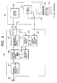
- the potential Vcc1 of the USB power supply portion (USB power supply line) 438 presents zero voltage, and the voltage Vcc1, which is zero volt, is transmitted to the output shut down circuit 413 in the power supply unit 401 through the signal line 425.
- the output shut down circuit 413 outputs to the feedback circuit 411 the signal that enables the voltage VD to be lowered to 5 volts or less. This signal is transmitted through the signal line 427. Further, the signal to lower the voltage is transmitted from the feedback circuit 411 to the switching circuit 409 through the signal line 423.
- the switching circuit 409 From the switching circuit 409 the signal that lowers the voltage output to 5 volts or less is transmitted to the power supply converting circuit 405 through the signal line 425.
- the voltage VD becomes 2.0 volts to 3.0 volts by way of the secondary rectification circuit 407. This is materialized by means of the intermittent oscillation of the voltage converting circuit 405 that contains a transformer.
- the output shut down circuit 413 may be allowed to execute the process to lower the voltage VD irrespective of the case where it is zero volt.
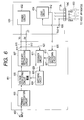
- Fig. 6 shows a third embodiment.
- Fig. 6 is the variation of the circuit structure shown in Fig. 2.
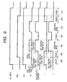
- the operation sequence thereof is shown in Fig. 5.
- the printing apparatus shown in Fig. 6 comprises a controller unit 630 and a power supply unit 601.
- the voltage VC is 24 volts or zero volt depending on the presence or absence of the AC input.
- the voltage of zero volt is transmitted to the output shut down circuit 613 in the power supply unit 601 through the signal line 642. Then, from the output shut down circuit 613, the signal that indicates the zero volt status is transmitted to the feedback circuit 611 through the signal line 627. Further, from the feedback circuit 611, the signal that indicates the zero volt status is transmitted to the switching circuit 609 through the signal line 623.
- this embodiment makes it possible to discriminate the driving conditions of the logic circuit by means of the CPU in the logic circuit 634 in addition to the effect demonstrated by the first embodiment as described earlier.
- the power control is effectuated to lower the dissipation power of the driving circuit as in the case of the standby mode.
- the control circuit containing a CPU, a storage, an ASIC, and the like, which operates by DC voltage of 5 volts, and the driving circuit that drives the driving sources, such as a carriage motor, a carrier motor, and a recording head, by the application of DC voltage of 24 volts.
- control circuit will be described as a logic circuit 834, and the driving circuit, as a power circuit 832.
- the printing apparatus can rise in a shorter period of time.
- the current i1 running to the diode 844 and the current i2 running to the diode 842 are joined together to supply the current of total 100 mA to the logic circuit 834.
- the logic circuit 834 consumes 100 mA
- the total current value of the current i1 and current i2 is 100 mA, and each of the current values is determined by the parameter of the circuit within a range of 0 mA to 100 mA.
- the printing apparatus When the operation mode is over, the printing apparatus returns to the standby mode 2 (708) again, and thereafter, the above cycle is repeated. Lastly, when the user removes the USB cable or the host computer is turned off, the USB power supply portion (USB power supply line) 838 becomes zero volt.
- the printing apparatus again returns to the standby mode 1 (the period at 714 in Fig. 7), and the controller 830 receives the supply of the current of voltage Vcc1 from the power supply unit 801.
- the power supply is effectuated for the control circuit, and with the supply capability of the 5-volt power supply circuit portion being confined to 100 mA, the secondary rectification circuit (2) 807' and the circuitry of the constant voltage circuit 832 are simplified to make the cost down possible.
- the power supply unit is structured to supply power with the control circuit being in the standby mode or standby mode 2. As a result, the power consumption is made lower. Further, when the USB cable is not connected with the host computer or even when the host computer is turned off, the printing apparatus can operate the initialization other than those for mechanical operations.
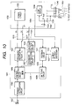
- Fig. 10 shows a fourth embodiment of the present invention.
- the control circuit containing a CPU, a storage, an ASIC, and the like, which operates by DC voltage of 5 volts, and the driving circuit that drives the driving sources, such as a carriage motor, a carrier motor, and a recording head, by the application of DC voltage of 24 volts.
- control circuit will be described as a logic circuit 1034, and the driving circuit, as a power circuit 1032.
- the power supply unit 1001 contains a primary rectification circuit 1003, a voltage converting circuit 1005, a secondary rectification circuit 1007, a switching circuit 1009, and a feedback circuit 1011.
- the switching circuit 1009 and the feedback circuit 1011 constitute a stable circuit that stabilizes voltage VD.
- the stabilizing control is the same as those of the first embodiment to the fourth embodiment. Therefore, the description will be omitted.
- the power supply unit 1001 generates two systems of voltage, that is, the voltage VD, which is the DC voltage, and 5 volts.
- the 5 volts is generated by means of the secondary rectification circuit (2) 1007', and the constant voltage circuit 1032.
- a switch (not shown) is turned on, the voltage VD is supplied to the power circuit 1032, and the 5-volt voltage is supplied to the logic circuit 1034.
- the switch is turned off, the power supplies to the power circuit 1032 and the logic circuit 1034 are cut off.
- an output shut down circuit 1002 is additionally provided in the power supply unit 1001. This circuit enables the CPU in the logic circuit 1034 to discriminate the standby mode and the operation mode and instruct the shut down circuit 1013 to lower the voltage VD during the period when the voltage VD is not needed (during the standby mode, for example).
- the Vcc1 voltage of zero volt is transmitted to the output shut down circuit 1013 in the power supply unit 1001 through the signal line 1042. From the output shut down circuit 1013, the signal that indicates the zero-volt state is transmitted to the feedback circuit 1011 through the signal line 1027. Further, the signal that indicates the zero-volt state is transmitted from the feedback circuit 1011 to the switching circuit 1009 through the signal line 1023.
- the switching circuit 1009 From the switching circuit 1009 the signal that lowers the voltage output to 2.0 to 3.0 volts, which is lower than 5 volts, is transmitted to the power supply converting circuit 1005 through the signal line 1025. As a result, the voltage VD becomes 2.0 volts to 3.0 volts by way of the secondary rectification circuit 1007. This is materialized by means of the intermittent oscillation of the voltage converting circuit 1005 that contains a transformer.
- this embodiment demonstrates the effect that the logic circuit is protected from the high voltage to be supplied to the driving circuit.
- the resolution of the recording head described in those embodiments is 600 dpi.
- the invention may be applicable to 1200 dpi and others without any problem.
- the method for discharging ink may also be the one that uses piezoelectric element.
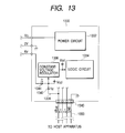
- a constant voltage regulator circuit 1336 may be provided between a diode and a logic circuit.
- the constant voltage regulator circuit 1336 generates the voltage of 3.3 volts with the input of 5-volt voltage from the connector 1340, thus making it possible to operate the logic circuit at 3.3 volts.
- the constant voltage regulator that can generate 2.5 volts from the voltage of 5 volts, it is also possible to materialize the operation of the logic circuit at 2.5 volts.
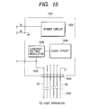
- the constant voltage regulator circuit 1536 generates 5 volts with the input of 12 volts from the connector 1540. In this manner, a logic circuit that can be driven at 5 volts is materialized. With the constant voltage regulator circuit that can generate 3.3 volts from 12 volts, it is also possible to materialize a logic circuit operable at 3.3 volts.
- the number of the IEEE1394 signal lines is four, which is more than that of the USB signal lines by two.
- the voltage inputted from the connector 1540 can be supplied to an output shut down circuit. Then, for example, the shut down circuit can recognize by use of the signal line 1538 that the Vp becomes zero volt.
- a structure can be materialized further to make supply possible from the logic circuit 1634 to the output shut down circuit by use of the signal line 1642.
- the voltage of the signal Vp of the IEEE1394 is not necessarily limited to 12 volts. There is no problem if it conforms to the IEEE1394 regulation within the voltage rage of 8 volts to 40 volts.
- the current value for use of the logic circuit, which is generated by the power supply unit, as described in the fourth and fifth embodiments is not necessarily limited to 100 mA.
- the input voltage to the power control circuit is not necessarily limited to 24 volts, either.
- the circuit that transmits signal to the feedback circuit for the suspension thereof is used as the output shut down circuit that drops off the voltage VD.
- signal may be output to the switching circuit if only it is suitably usable for controlling the stable circuit.
- the power supplied from the interface is utilized as the power source that drives the control circuit of the printing apparatus in accordance with the present invention.
- the power supply to the printing apparatus is dedicated for driving the driving source, such as a recording head, motors, hence making it possible to materialize a smaller power supply circuit, and cost down as well.
Landscapes
- Accessory Devices And Overall Control Thereof (AREA)
- Ink Jet (AREA)
- Power Sources (AREA)
- Direct Current Feeding And Distribution (AREA)
Abstract
Description
Claims (14)
- An ink jet recording apparatus provided with a control circuit for controlling the recording operation using a recording head, and a driving circuit for driving the driving source to drive the recording head, comprising:the power supply portion of a serial interface to supply power to said control circuit with a first voltage value;a second voltage output circuit for supplying power to said driving circuit with a second voltage value.
- An ink jet recording apparatus provided with a control circuit for controlling the recording operation using a recording head, and, a driving circuit for driving the driving source to drive the recording head, comprising:the power supply portion of a serial interface to supply power to said control circuit with a first voltage value;a power supply unit having a first voltage output circuit for supplying power to said control circuit with a first voltage value, and a second voltage output circuit for supplying power to said driving circuit with a second voltage value, whereinthe power supply to said control circuit from said first output circuit and said power supply portion of said serial interface is executed in accordance with the status of the power supply portion of said serial interface.
- An ink jet recording apparatus according to Claim 2, wherein a diode for use of reverse current prevention is connected between said first voltage output circuit and the power supply portion of said serial interface.
- An ink jet recording apparatus according to Claim 3, wherein a constant voltage regulator is connected between said control circuit and said diode for use of reverse current prevention.
- An ink jet recording apparatus according to either one of Claim 2 to Claim 4, wherein the maximum current value generated by said first voltage output circuit is the maximum value of current consumption of said control circuit in the standby mode of the ink jet recording apparatus.
- An ink jet recording apparatus according to Claim 1 or Claim 2, wherein a constant voltage regulator is connected between said control circuit and the power supply portion of said serial interface.
- An ink jet recording apparatus according to either one of Claim 1 to Claim 6, wherein when said apparatus is in a designated status, said control circuit issues to said power supply unit an instruction signal for lowering said second voltage output to a designated voltage, and said power supply unit lowers said second voltage output to a designated voltage.
- An inkjet recording apparatus according to either one of Claim 1 to Claim 7, wherein said second voltage output circuit is provided with a stabilizing circuit for stabilizing said second voltage with feedback thereto.
- An ink jet recording apparatus according to Claim 8, wherein said power supply unit is provided with an output shut down circuit between said stabilizing circuit and the power supply portion of said serial interface, and when the voltage of said power supply portion does not reach a designated potential, said output shut down circuit issues signal to said stabilizing circuit, and said stabilizing circuit lowers said second voltage output to a designated voltage.
- An ink jet recording apparatus according to either one of Claim 1 to Claim 9, wherein said serial interface is an interface conforming to or being in accordance with the IEEE1394 regulation.
- An ink jet recording apparatus according to either one of Claim 1 to Claim 9, wherein said serial interface is an interface conforming to or being in accordance with the USB regulation.
- An ink jet recording apparatus according to either one of Claim 1 to Claim 11, wherein said recording head is provided with a plurality of recording elements containing electrothermal converting members to generate thermal energy as energy for discharging ink.
- A method for controlling an ink jet recording apparatus provided with a control circuit for controlling the recording operation using a recording head, and a driving circuit to drive the recording head, comprising the following steps of:operating said control circuit in said recording operation with the power supply from the power supply portion of a serial interface with a first voltage value; andoperating said driving circuit by the power supply from said power supply unit with a second voltage value.
- A method for controlling an ink jet recording apparatus according to Claim 13, wherein said operation of control circuit executes a process to lower said second voltage output to a designated voltage when the step thereof presents a designated condition.
Applications Claiming Priority (2)
| Application Number | Priority Date | Filing Date | Title |
|---|---|---|---|
| JP2001129743A JP3652274B2 (en) | 2001-04-26 | 2001-04-26 | Ink jet recording apparatus and recording apparatus control method |
| JP2001129743 | 2001-04-26 |
Publications (2)
| Publication Number | Publication Date |
|---|---|
| EP1254772A1 true EP1254772A1 (en) | 2002-11-06 |
| EP1254772B1 EP1254772B1 (en) | 2004-07-07 |
Family
ID=18978225
Family Applications (1)
| Application Number | Title | Priority Date | Filing Date |
|---|---|---|---|
| EP02009593A Expired - Lifetime EP1254772B1 (en) | 2001-04-26 | 2002-04-26 | Ink jet recording apparatus and controlling method for recording apparatus |
Country Status (6)
| Country | Link |
|---|---|
| US (1) | US6749278B2 (en) |
| EP (1) | EP1254772B1 (en) |
| JP (1) | JP3652274B2 (en) |
| KR (1) | KR100464743B1 (en) |
| CN (1) | CN1172229C (en) |
| DE (1) | DE60200704T2 (en) |
Families Citing this family (17)
| Publication number | Priority date | Publication date | Assignee | Title |
|---|---|---|---|---|
| KR100422008B1 (en) * | 2002-06-25 | 2004-03-11 | 삼성전자주식회사 | Laser beam printer having stability output of laser beam |
| JP2004202692A (en) * | 2002-12-20 | 2004-07-22 | Canon Finetech Inc | Image formation device |
| TWI246462B (en) * | 2003-06-10 | 2006-01-01 | Canon Kk | Ink-jet printhead substrate, driving control method, ink-jet printhead and ink-jet printing apparatus |
| KR20050106745A (en) * | 2004-05-06 | 2005-11-11 | 삼성전자주식회사 | Apparatus for supplying power in portable device |
| JP4861981B2 (en) * | 2004-07-23 | 2012-01-25 | トムソン ライセンシング | System and method for reducing standby power consumption |
| JP2006231635A (en) * | 2005-02-23 | 2006-09-07 | Seiko Epson Corp | Liquid ejector |
| US8126348B2 (en) * | 2006-02-06 | 2012-02-28 | Samsung Electronics Co., Ltd. | Printing apparatus to reduce power consumption and control method thereof |
| US8228092B2 (en) * | 2006-09-15 | 2012-07-24 | Texas Instruments Northern Virginia Incorporated | High voltage latching and DC restoration isolation and level shifting method and apparatus |
| JP2008225993A (en) * | 2007-03-14 | 2008-09-25 | Pfu Ltd | Power supply control circuit and scanner device |
| JP5111198B2 (en) * | 2007-05-01 | 2012-12-26 | キヤノン株式会社 | Element substrate, recording head, head cartridge, and recording apparatus |
| US8198757B2 (en) * | 2009-03-04 | 2012-06-12 | International Business Machines Corporation | Energy savings for a system powering a lower voltage device from a higher voltage power source, and wherein the system includes a power plug that outputs power to a converter, and a switch actuator |
| JP5574629B2 (en) * | 2009-06-22 | 2014-08-20 | キヤノン株式会社 | Equipment with power supply circuit |
| JP2011234573A (en) * | 2010-04-28 | 2011-11-17 | Toshiba Corp | Information processor and method for controlling the same |
| JP6247452B2 (en) * | 2013-05-02 | 2017-12-13 | キヤノン株式会社 | Recording head and recording apparatus |
| JP6364826B2 (en) * | 2014-03-07 | 2018-08-01 | セイコーエプソン株式会社 | Recording apparatus and recording method |
| US9636908B2 (en) * | 2014-09-30 | 2017-05-02 | Brother Kogyo Kabushiki Kaisha | Liquid discharging apparatus |
| JP2024029867A (en) | 2022-08-23 | 2024-03-07 | セイコーエプソン株式会社 | liquid dispensing system |
Citations (4)
| Publication number | Priority date | Publication date | Assignee | Title |
|---|---|---|---|---|
| WO1998008157A2 (en) * | 1996-08-19 | 1998-02-26 | Jouni Rudvin A/S | Paper drive for portable computer |
| JPH10226139A (en) * | 1997-02-14 | 1998-08-25 | Canon Inc | Image forming system, image forming apparatus, and medium |
| JPH11353061A (en) * | 1998-06-09 | 1999-12-24 | Casio Electronics Co Ltd | Power control device |
| EP1078752A2 (en) * | 1999-08-24 | 2001-02-28 | Canon Kabushiki Kaisha | Printhead and printing apparatus using the same |
Family Cites Families (10)
| Publication number | Priority date | Publication date | Assignee | Title |
|---|---|---|---|---|
| EP0374762B1 (en) | 1988-12-16 | 1995-03-15 | Canon Kabushiki Kaisha | Recording apparatus to which recording head is detachably mountable |
| JP2820579B2 (en) * | 1992-10-20 | 1998-11-05 | 沖電気工業株式会社 | Terminal control device |
| US5617122A (en) | 1992-12-10 | 1997-04-01 | Canon Kabushiki Kaisha | Recording apparatus and method for controlling recording head driving timing |
| KR950007112B1 (en) * | 1993-06-25 | 1995-06-30 | 현대전자주식회사 | Power control device of printer |
| JP2795170B2 (en) * | 1994-03-31 | 1998-09-10 | 日本電気株式会社 | Ink jet recording head and method of manufacturing the same |
| KR200149606Y1 (en) * | 1996-05-15 | 1999-06-15 | Samsung Electronics Co Ltd | Power controlling device for printer |
| JPH10250191A (en) * | 1997-03-11 | 1998-09-22 | Canon Inc | Output device and power supply method |
| JP3446533B2 (en) * | 1997-05-12 | 2003-09-16 | 富士ゼロックス株式会社 | Ink jet recording head and method of manufacturing the same |
| JP3360665B2 (en) * | 1999-03-12 | 2002-12-24 | セイコーエプソン株式会社 | Electronic printing apparatus having power saving mode and control method |
| JP2002036668A (en) * | 2000-07-24 | 2002-02-06 | Brother Ind Ltd | Printer |
-
2001
- 2001-04-26 JP JP2001129743A patent/JP3652274B2/en not_active Expired - Fee Related
-
2002
- 2002-04-23 US US10/127,435 patent/US6749278B2/en not_active Expired - Fee Related
- 2002-04-26 DE DE60200704T patent/DE60200704T2/en not_active Expired - Lifetime
- 2002-04-26 EP EP02009593A patent/EP1254772B1/en not_active Expired - Lifetime
- 2002-04-26 CN CNB021218080A patent/CN1172229C/en not_active Expired - Fee Related
- 2002-04-26 KR KR10-2002-0022911A patent/KR100464743B1/en not_active Expired - Fee Related
Patent Citations (4)
| Publication number | Priority date | Publication date | Assignee | Title |
|---|---|---|---|---|
| WO1998008157A2 (en) * | 1996-08-19 | 1998-02-26 | Jouni Rudvin A/S | Paper drive for portable computer |
| JPH10226139A (en) * | 1997-02-14 | 1998-08-25 | Canon Inc | Image forming system, image forming apparatus, and medium |
| JPH11353061A (en) * | 1998-06-09 | 1999-12-24 | Casio Electronics Co Ltd | Power control device |
| EP1078752A2 (en) * | 1999-08-24 | 2001-02-28 | Canon Kabushiki Kaisha | Printhead and printing apparatus using the same |
Non-Patent Citations (2)
| Title |
|---|
| PATENT ABSTRACTS OF JAPAN vol. 1998, no. 13 30 November 1998 (1998-11-30) * |
| PATENT ABSTRACTS OF JAPAN vol. 2000, no. 03 30 March 2000 (2000-03-30) * |
Also Published As
| Publication number | Publication date |
|---|---|
| JP3652274B2 (en) | 2005-05-25 |
| CN1382585A (en) | 2002-12-04 |
| KR100464743B1 (en) | 2005-01-06 |
| DE60200704T2 (en) | 2005-07-14 |
| US20020171694A1 (en) | 2002-11-21 |
| KR20020083936A (en) | 2002-11-04 |
| JP2002321347A (en) | 2002-11-05 |
| US6749278B2 (en) | 2004-06-15 |
| CN1172229C (en) | 2004-10-20 |
| EP1254772B1 (en) | 2004-07-07 |
| DE60200704D1 (en) | 2004-08-12 |
Similar Documents
| Publication | Publication Date | Title |
|---|---|---|
| EP1254772B1 (en) | Ink jet recording apparatus and controlling method for recording apparatus | |
| US7538502B2 (en) | Motor driver circuit, control method thereof, and electronic apparatus | |
| JPS6126319B2 (en) | ||
| JP2006271028A (en) | Power supply device and image forming apparatus | |
| EP0997811B1 (en) | Electronic apparatus and method for controlling supply of power for electronic apparatus, | |
| KR100519688B1 (en) | Ink jet recording device and controlling method therefor | |
| US7290847B2 (en) | IC chip, print apparatus, and heat generation warning method | |
| US20040183840A1 (en) | Battery residual capacity detection method and printing apparatus using the method | |
| JP3337709B2 (en) | Charge control device, control method of the device, electronic device, and control method of electronic device | |
| EP0916511A2 (en) | Recording apparatus having a charging function, and charging method | |
| US20130194841A1 (en) | Power supply apparatus and printing apparatus | |
| JP2002178610A (en) | Printer control device | |
| US6761424B2 (en) | Image print apparatus and control method thereof | |
| US10668718B2 (en) | Inkjet recording apparatus and method for controlling an inkjet recording apparatus | |
| US8664799B2 (en) | Apparatus including power supply circuit | |
| US7596166B2 (en) | Integrated circuit device including a spectrum spread clock generator, method for controlling the device, and ink-jet recording apparatus including the device | |
| KR100233674B1 (en) | Apparatus and method for protecting recording head ina multi function product used ink jet process | |
| JP3428981B2 (en) | Electronics | |
| JP2006352978A (en) | MOTOR DRIVER CIRCUIT, METHOD FOR CONTROLLING THE CIRCUIT, ELECTRONIC DEVICE, AND MOTOR LOCK DETECTION METHOD FOR ELECTRONIC DEVICE | |
| JP2008260130A (en) | Printer apparatus | |
| JPH07205526A (en) | Power supply controller of printer | |
| JP2008140233A (en) | Electronics | |
| JP2016134059A (en) | Power supply apparatus, printing apparatus, and control method for power supply apparatus | |
| JP2005131990A (en) | Recording device | |
| JPH05227751A (en) | Power supply |
Legal Events
| Date | Code | Title | Description |
|---|---|---|---|
| PUAI | Public reference made under article 153(3) epc to a published international application that has entered the european phase |
Free format text: ORIGINAL CODE: 0009012 |
|
| AK | Designated contracting states |
Kind code of ref document: A1 Designated state(s): AT BE CH CY DE DK ES FI FR GB GR IE IT LI LU MC NL PT SE TR |
|
| AX | Request for extension of the european patent |
Free format text: AL;LT;LV;MK;RO;SI |
|
| 17P | Request for examination filed |
Effective date: 20030319 |
|
| AKX | Designation fees paid |
Designated state(s): DE FR GB IT |
|
| GRAP | Despatch of communication of intention to grant a patent |
Free format text: ORIGINAL CODE: EPIDOSNIGR1 |
|
| GRAS | Grant fee paid |
Free format text: ORIGINAL CODE: EPIDOSNIGR3 |
|
| GRAA | (expected) grant |
Free format text: ORIGINAL CODE: 0009210 |
|
| AK | Designated contracting states |
Kind code of ref document: B1 Designated state(s): DE FR GB IT |
|
| REG | Reference to a national code |
Ref country code: GB Ref legal event code: FG4D |
|
| REG | Reference to a national code |
Ref country code: IE Ref legal event code: FG4D |
|
| REF | Corresponds to: |
Ref document number: 60200704 Country of ref document: DE Date of ref document: 20040812 Kind code of ref document: P |
|
| ET | Fr: translation filed | ||
| PLBE | No opposition filed within time limit |
Free format text: ORIGINAL CODE: 0009261 |
|
| STAA | Information on the status of an ep patent application or granted ep patent |
Free format text: STATUS: NO OPPOSITION FILED WITHIN TIME LIMIT |
|
| 26N | No opposition filed |
Effective date: 20050408 |
|
| PGFP | Annual fee paid to national office [announced via postgrant information from national office to epo] |
Ref country code: FR Payment date: 20090424 Year of fee payment: 8 Ref country code: IT Payment date: 20090415 Year of fee payment: 8 |
|
| REG | Reference to a national code |
Ref country code: FR Ref legal event code: ST Effective date: 20101230 |
|
| PG25 | Lapsed in a contracting state [announced via postgrant information from national office to epo] |
Ref country code: IT Free format text: LAPSE BECAUSE OF NON-PAYMENT OF DUE FEES Effective date: 20100426 |
|
| PGFP | Annual fee paid to national office [announced via postgrant information from national office to epo] |
Ref country code: DE Payment date: 20110430 Year of fee payment: 10 |
|
| PGFP | Annual fee paid to national office [announced via postgrant information from national office to epo] |
Ref country code: GB Payment date: 20110413 Year of fee payment: 10 |
|
| PG25 | Lapsed in a contracting state [announced via postgrant information from national office to epo] |
Ref country code: FR Free format text: LAPSE BECAUSE OF NON-PAYMENT OF DUE FEES Effective date: 20100430 |
|
| GBPC | Gb: european patent ceased through non-payment of renewal fee |
Effective date: 20120426 |
|
| PG25 | Lapsed in a contracting state [announced via postgrant information from national office to epo] |
Ref country code: GB Free format text: LAPSE BECAUSE OF NON-PAYMENT OF DUE FEES Effective date: 20120426 |
|
| REG | Reference to a national code |
Ref country code: DE Ref legal event code: R119 Ref document number: 60200704 Country of ref document: DE Effective date: 20121101 |
|
| PG25 | Lapsed in a contracting state [announced via postgrant information from national office to epo] |
Ref country code: DE Free format text: LAPSE BECAUSE OF NON-PAYMENT OF DUE FEES Effective date: 20121101 |