EP1253597A1 - Method and circuit for generating reference voltages for reading a multilevel memory cell - Google Patents
Method and circuit for generating reference voltages for reading a multilevel memory cell Download PDFInfo
- Publication number
- EP1253597A1 EP1253597A1 EP01830276A EP01830276A EP1253597A1 EP 1253597 A1 EP1253597 A1 EP 1253597A1 EP 01830276 A EP01830276 A EP 01830276A EP 01830276 A EP01830276 A EP 01830276A EP 1253597 A1 EP1253597 A1 EP 1253597A1
- Authority
- EP
- European Patent Office
- Prior art keywords
- circuit
- voltage
- charge
- current
- memory cell
- Prior art date
- Legal status (The legal status is an assumption and is not a legal conclusion. Google has not performed a legal analysis and makes no representation as to the accuracy of the status listed.)
- Granted
Links
- 230000015654 memory Effects 0.000 title claims abstract description 57
- 238000000034 method Methods 0.000 title claims description 18
- 239000003990 capacitor Substances 0.000 claims description 51
- 238000007599 discharging Methods 0.000 claims description 4
- 230000010354 integration Effects 0.000 description 27
- 238000011069 regeneration method Methods 0.000 description 19
- 238000010586 diagram Methods 0.000 description 6
- 230000008569 process Effects 0.000 description 5
- 230000002596 correlated effect Effects 0.000 description 4
- 230000009467 reduction Effects 0.000 description 4
- 238000006243 chemical reaction Methods 0.000 description 3
- 230000000875 corresponding effect Effects 0.000 description 3
- 230000003071 parasitic effect Effects 0.000 description 3
- 238000009826 distribution Methods 0.000 description 2
- 230000004048 modification Effects 0.000 description 2
- 238000012986 modification Methods 0.000 description 2
- 238000004513 sizing Methods 0.000 description 2
- 230000008901 benefit Effects 0.000 description 1
- 230000000694 effects Effects 0.000 description 1
- 238000005516 engineering process Methods 0.000 description 1
- 230000006870 function Effects 0.000 description 1
- 238000004519 manufacturing process Methods 0.000 description 1
- 239000002184 metal Substances 0.000 description 1
- 230000035945 sensitivity Effects 0.000 description 1
Images


Classifications
-
- G—PHYSICS
- G11—INFORMATION STORAGE
- G11C—STATIC STORES
- G11C11/00—Digital stores characterised by the use of particular electric or magnetic storage elements; Storage elements therefor
- G11C11/56—Digital stores characterised by the use of particular electric or magnetic storage elements; Storage elements therefor using storage elements with more than two stable states represented by steps, e.g. of voltage, current, phase, frequency
-
- G—PHYSICS
- G11—INFORMATION STORAGE
- G11C—STATIC STORES
- G11C11/00—Digital stores characterised by the use of particular electric or magnetic storage elements; Storage elements therefor
- G11C11/56—Digital stores characterised by the use of particular electric or magnetic storage elements; Storage elements therefor using storage elements with more than two stable states represented by steps, e.g. of voltage, current, phase, frequency
- G11C11/5621—Digital stores characterised by the use of particular electric or magnetic storage elements; Storage elements therefor using storage elements with more than two stable states represented by steps, e.g. of voltage, current, phase, frequency using charge storage in a floating gate
-
- G—PHYSICS
- G11—INFORMATION STORAGE
- G11C—STATIC STORES
- G11C11/00—Digital stores characterised by the use of particular electric or magnetic storage elements; Storage elements therefor
- G11C11/56—Digital stores characterised by the use of particular electric or magnetic storage elements; Storage elements therefor using storage elements with more than two stable states represented by steps, e.g. of voltage, current, phase, frequency
- G11C11/5621—Digital stores characterised by the use of particular electric or magnetic storage elements; Storage elements therefor using storage elements with more than two stable states represented by steps, e.g. of voltage, current, phase, frequency using charge storage in a floating gate
- G11C11/5642—Sensing or reading circuits; Data output circuits
-
- G—PHYSICS
- G11—INFORMATION STORAGE
- G11C—STATIC STORES
- G11C5/00—Details of stores covered by group G11C11/00
- G11C5/14—Power supply arrangements, e.g. power down, chip selection or deselection, layout of wirings or power grids, or multiple supply levels
- G11C5/147—Voltage reference generators, voltage or current regulators; Internally lowered supply levels; Compensation for voltage drops
-
- G—PHYSICS
- G11—INFORMATION STORAGE
- G11C—STATIC STORES
- G11C2211/00—Indexing scheme relating to digital stores characterized by the use of particular electric or magnetic storage elements; Storage elements therefor
- G11C2211/56—Indexing scheme relating to G11C11/56 and sub-groups for features not covered by these groups
- G11C2211/563—Multilevel memory reading aspects
- G11C2211/5634—Reference cells
Definitions
- the present invention relates to a method and a circuit for generating reference voltages for reading a multilevel memory cell.
- Reading of multi-level cells is carried out evaluating the current or the voltage.
- Current reading is based on comparing the current flowing in a cell at a preset gate voltage Vgs and the current flowing in a reference cell, the characteristic of which is intermediate between the distributions of the programmed cells, as shown in Figure 2.
- the comparison is made after a current-to-voltage conversion, both of the current of the cell and of the reference current.
- US-A-6 034 888 proposes a voltage reading method using a closed-loop circuit (see Figure 5).
- this circuit the current of the cell to be read is compared with a reference current, and the gate voltage of the cell is modulated until reaching the equilibrium of the system. Thereby, the gate voltage of the cell reaches a value that can be defined as the threshold value of the cell.
- a memory cell is represented by a current source 10, which is connected between a ground line or connection (hereinafter referred to as ground line 19) and a charge-transfer node 11.
- the current source 10 has a control node 10a receiving a first control signal s and absorbs a constant current I directed towards the ground line 19, when enabled by the first control signal s.
- the charge-transfer node 11 is connected to a reading circuit 20 comprising a decoupling stage 21, a charge-regeneration capacitor 22 having a capacitance Ca, and an integration capacitor 23 having a capacitance Cb.
- the decoupling stage 21, formed by a circuit known as "cascode”, comprises an inverting element, here an inverter 24, having an input connected to the charge-transfer node 11 and an output connected to the gate terminal of a cascode transistor 25, of NMOS type.
- the cascode transistor 25 moreover has a source terminal connected to the charge-transfer node 11 and a drain terminal connected to the drain terminal of a pass transistor 27, of NMOS type.
- the pass transistor 27 has a gate terminal receiving a second control signal Vp and a drain terminal connected to a charge-integration node 28.
- the charge-regeneration capacitor 22 has a first terminal 22a connected to the charge-integration node 28 and a second terminal 22b connected to the ground line 19.
- the charge-integration node 28 is connected to the drain terminal of a charge transistor 29, of PMOS type.
- the charge transistor 29 has a source terminal connected to a biasing line 30 set at a bias voltage Vpcx and a gate terminal receiving a charge-enabling signal en.
- the bias voltage Vpcx can be either a standard supply voltage (e.g. of 3 V) or a boosted voltage (e.g. of 6 V) provided by a boosting device of a known type and not shown herein.
- the charge-integration node 28 forms the output of the reading circuit 20, and generates a voltage Va proportional, as will be explained hereinafter, to the current I flowing in the current source 10.
- a voltage Vb is present on the charge-transfer node 11.
- the voltages Va and Vb on the charge-integration node 28 and on the charge-transfer node 11 are low.
- the first control signal s keeps the current source 10 off.
- the charge-enabling signal en is low and keeps the charge transistor 29 on.
- the second control signal Vp is high and keeps the pass transistor 27 on.
- the output of the inverter 24 is high, and the cascode transistor 25 is on and enables charging of the integration capacitor 23 up to the threshold voltage of the inverter 24.
- V ai the value of the voltage V a at the end of the charging step
- Q ai the charge stored in the charge-regeneration capacitor 22
- V bi the value of the voltage V b at the end of the charging step
- Q bi the charge stored in the integration capacitor 23.
- the charge-enabling signal en switches to the high state (Vpcx) and turns off the charge transistor 29 (in this way isolating the charge-regeneration capacitor 22 from the supply line 30).
- the second control signal Vp switches to low and turns off the pass transistor 27 (thereby isolating the charge-transfer node 11 and the charge-integration node 28).
- the first control signal s switches and turns on the current source 10, which, to a first approximation, goes to a steady-state condition in a negligibly small time, so that the integration capacitor 23 will not be affected by current transients.
- the second control signal Vp switches again to high, turning on the pass transistor 27 and connecting together, through the decoupling stage 21, the charge-integration node 28 and the charge-transfer node 11. Consequently, the charge-regeneration capacitor 22 discharges rapidly to the integration capacitor 23, re-integrating the charge lost by the latter, according to a charge-sharing process.
- the charge-regeneration capacitor 22 operates as a charge reservoir. However, the charge-integration node 28 and the charge-transfer node 11 do not assume the same potential.
- the decoupling stage 21 allows the charge-transfer node 11 to reach only the value of the triggering voltage of the inverter 24, after which the inverter 24 turns on the cascode transistor 25, thus once again isolating the charge-integration node 28 from the charge-transfer node 11.
- the final voltage on the charge-regeneration capacitor 22 is equal to V af
- the final charge of the charge-regeneration capacitor 22 is equal to Q af
- the charge transferred from the charge-regeneration capacitor 22 to the integration capacitor 23 is ⁇ Q a , equal to the charge ⁇ Qb lost by the charge-regeneration capacitor (which has returned to the initial conditions).
- V bf V bi
- Relation (2) makes it possible to distinguish very small current variations from one another by measuring the voltage difference ⁇ Va that may be obtained on the charge-integration node 28.
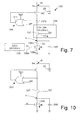
- Figure 7 shows a circuit 135 that implements the current source 10 of Figure 5 and comprises a memory cell 136.
- a memory cell 136 in particular a nonvolatile memory cells such a flash cell, has a source terminal 136a connected to the ground line 19, a gate terminal 136b biased at a read voltage Vr via a row decoder 139 (shown only schematically), and a drain terminal 136c connected to the source terminal of a decoding transistor 137 belonging to a column decoder, which is shown only schematically.
- the read voltage Vr is a boosted voltage Vdd, for example 6 V.
- the decoding transistor 137 has a gate terminal 137a receiving a column enable signal Vyo, and a drain terminal 137b connected to the charge-transfer node 11 through a biasing circuit 140 implemented by a controllable cascode circuit.
- the biasing circuit 140 comprises a NOR gate 141 and a decoupling transistor 142.
- the NOR gate 141 has a first input receiving a turning-on signal csm, a second input connected to the drain terminal 137b of the decoding transistor 137, and an output connected to the gate terminal of the decoupling transistor 142.
- the decoupling transistor 142 which is of NMOS type, has a source terminal connected to the drain terminal 137b of the decoding transistor 137 and a drain terminal connected to the charge-transfer node 11.
- Figure 7 moreover shows a column capacitor 145 representing the capacitance associated to the bit line connected to the memory cell 136 and the second capacitor 23 of Figure 5.
- the gate terminal 136b of the memory cell 136 is biased at the read voltage Vr (for example, 6 V). Only after the gate terminal 136b has reached the steady-state value (which in current flash memories requires a few tens of nanoseconds) does the column enable signal Vyo switch from 0 V to a high value (for example 3 V), so turning on the decoding transistor 137, which takes place in a few nanoseconds.
- Vr read voltage
- the turning-on signal csm is low and enables the biasing circuit 140.
- the latter given its cascode structure, keeps the voltage on the drain terminal 137b of the decoding transistor 137 constant, and hence the voltage V1 on the drain terminal 136c of the memory cell 136 also constant, and approximately at 1 V.
- the memory cell 136 absorbs a constant current and the second capacitor 23 discharges linearly as long as the column enable signal Vyo remains high.
- the circuit 135 thus effectively operates as a constant-current source and is equivalent to the source 110, with I being the current flowing through the memory cell 136; in addition, the column enable signal Vyo in practice implements the first control signal s of Figure 5.
- the read circuit described above thus enables discrimination, in a short time, of programming states that are very close to one another, in practice enabling increase in the number of bits that may be stored in a cell (for example, four bits, corresponding to 16 programming levels), but has a number of drawbacks. It is known, in fact, that, given the same programming level, the current flowing in a nonvolatile memory cell depends upon a plurality of factors of disturbance, such as the temperature, fluctuations in the supply voltage, and non-controllable variations in process parameters. Consequently, also the voltage Va on the charge-integration node 28 at the end of the charge-sharing step is not constant, and hence reading errors may occur.
- the voltage Va on the charge-integration node 28 must be converted into a numeric signal correlated to the level of programming of the memory cell that is to be read.
- an analog-to-digital converter is used that compares the voltage Va with a plurality of reference voltages, each of which indicates a respective programming level.
- the voltage Va generated by reading of a memory cell having a given programming level may vary not only in an absolute sense, but also in relation to the reference voltages of the A-D converter. Consequently, it may happen that the reference voltage closest to the voltage Va on the charge-integration node 28 is representative of a programming level other than that of the memory cell that is being read. It is clear that, in this case, the programming level of the memory cell is not correctly recognized, and a reading error occurs.
- the purpose of the present invention is therefore to provide a circuit for generating reference voltages that will enable the limitations described previously to be overcome.
- a method and a circuit for generating reference voltages for reading a multilevel memory cell are provided, as defined respectively in Claim 1 and Claim 7.
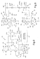
- a memory device 35 comprises an array 40 of memory cells, one of which is here illustrated schematically by the current generator 10; in addition, the memory device 35 includes the read circuit 20 of Figure 5, which will not be further described herein, an analog-to-digital converter 41, and a reference generating stage 42.
- the A-D converter 41 has a signal input 41a connected to the charge-integration node 28 and a plurality of reference inputs, which are connected to respective output terminals 42.1, 42.2,..., 42.N-1 of the reference generating stage 42.
- the A-D converter has an output 41b supplying a numerical signal D, which is correlated to the programming level of a memory cell to be read, and hence to the current I flowing in the current generator 10, as already mentioned.
- N designates the possible programming levels of the memory cells of the memory device 35
- the number of the output terminals 42.1, 42.2,..., 42.N-1 of the reference generating stage 42 and the number of the reference inputs of the A-D converter 41 are equal to N - 1.
- the reference generating stage 42 supplies, on its own output terminals 42.1, 42.2,..., 42.N-1, respective reference voltages VR1, VR2,..., VRN-1, each of which represents a respective programming level.
- the reference voltages VR1, VR2,..., VRN-1 decrease in an orderly manner from the maximum reference voltage VR1 to the minimum reference voltage VRN-1 and are at equal distances apart.
- the reference generating stage 42 comprises a first reference current generator 44 and a second reference current generator 45, a first reference circuit 46 and a second reference circuit 47, a voltage divider 48, and a first follower stage 49 and a second follower stage 50.
- the reference current generators 44, 45 represent memory cells, as described in what follows with reference to Figure 10.
- each of the reference circuits 46, 47 comprises a reference integration capacitor 53, which has a capacitance Cb and is connected between the ground line 19 and a reference transfer node 54; a decoupling stage 55, made up of a reference cascode transistor 56, which has its source terminal connected to the reference transfer node 54, and a reference inverter 57 connected between the source terminal and the gate terminal of the reference cascode transistor 56; a reference pass transistor 59, which has its source terminal connected to the drain terminal of the reference cascode transistor 56, its drain terminal connected to a reference integration node 60, and its gate terminal receiving the second control signal Vp; a reference charge transistor 61, which has its source terminal and drain terminal respectively connected to the biasing line 30 and to the reference integration node 60, and receives on its own gate terminal the charge-enable signal en; and a reference charge-regeneration capacitor 61, which has a capacitance Ca
- the first reference current generator 44 is connected between the ground line 19 and the reference transfer node 54 of the first reference circuit 46, and has a control terminal 44a which receives the first control signal s. When activated, the first reference current generator 44 absorbs a first reference current IR1.
- the second reference current generator 45 is connected between the ground line 19 and the reference transfer node 54 of the second reference circuit 47, and has a control terminal 45a which receives the first control signal s. When activated, the second reference current generator 45 absorbs a second reference current IR2.
- the voltage divider 48 comprises a plurality of resistors 51 which have equal resistances and are connected in series between the output terminals 42.1, 42.2,..., 42.N-1 of the reference generating circuit 42.
- the intermediate nodes, or “taps", between pairs of resistors 51 form, instead, the intermediate output terminals 42.2, ..., 42.N-2 of the reference generating circuit 42.
- the output terminal 42.1 is connected to the reference integration node 60 of the first reference circuit 46 via the first follower stage 49
- the output terminal 42.N-1 is connected to the reference integration node 60 of the second reference circuit 47 via the second follower stage 50.
- the follower stages 49, 50 comprise respective operational amplifiers each having a non-inverting input respectively connected to the reference integration node 60 of the first reference circuit 46 and to the reference integration node 60 of the second reference circuit 47, and an output connected to the respective inverting input and respectively defining the output terminal 42.1 and the output terminal 42.N-1.
- each reference current generator 44, 45 is built as shown in Figure 5 and have the same structure as the current generator 10 shown in Figure 7.
- each reference current generator 44, 45 comprises a reference memory cell 236, in particular a nonvolatile memory cell, such as a flash cell, connected between the ground line 19 and a transistor 237 simulating the decoding transistor 137 of the column decoder 138 ( Figure 7).
- the gate terminal of the reference memory cell 236 is biased at a read voltage Vr.
- the transistor 237 has its gate terminal that receives the enabling voltage Vyo and is connected to the reference transfer node 54 via a biasing circuit 240.
- a capacitor 245 also in this case represents the capacitance associated to the line to which the memory cell 236 is connected.
- the current IR flowing in the reference memory cell 236 is constant and correlated to the programming level of the reference memory cell 236.
- the desired current levels IR1, IR2 absorbed by the reference current generators 44, 45 may thus be obtained by appropriately programming the respective reference memory cells 236 during the electrical-wafer-sort (EWS) step.
- the memory cell 136 represented schematically by the current generator 10 is read using the procedure already described with reference to Figure 6.
- a voltage Va correlated to the programming level of the memory cell to be read is therefore supplied on the charge-integration node 28.
- the reference cells 236, one of which is represented schematically by the first reference current generator 44 and the other by the second reference current generator 45, are read using a similar procedure.
- first a step is performed for charging the reference integration capacitor 53 and the reference charge-regeneration capacitor 62 ( Figure 6, instant t1).
- the reference transfer nodes 54 of each of the reference branches 46, 47 are then isolated from the respective reference integration nodes 60 by turning off the pass transistors 59 (instant t2), and, subsequently, the first reference current generator 44 and the second reference current generator 45 are activated (instant t3).
- the charge-regeneration capacitors 62 of the first reference circuit 46 and second reference circuit 47 are discharged linearly respectively with the first reference current IR1 and the second reference current IR2 (step of integration of the currents IR1, IR2) up to the pre-set instant t4, at which the reference current generators 44, 45 are deactivated.
- a charge-sharing step is carried out (instant t5), during which the charge lost by the integration capacitors 53 of the first reference circuit 46 and second reference circuit 47 is restored using the charge present in the respective charge-regeneration capacitors 62.
- the reference transfer nodes 54 of the first reference circuit 46 and second reference circuit 47 there are respectively present the maximum reference voltage VR1 and the minimum reference voltage VRN-1.
- the said maximum reference voltage VR1 and minimum reference voltage VRN-1 are respectively supplied to the output terminals 42.1 and 42.N-1 of the reference generating circuit 42. Consequently, on the intermediate output nodes 42.2, ..., 42.N-2 of the reference generating circuit 42 there are present the intermediate reference voltages VR2, ..., VRN-2, which are at equal distances apart.
- the currents absorbed by the cells 136, 236, and hence also the voltages present in the memory device 35 may depart from the nominal values.
- these variations normally affect the entire memory device 35 uniformly.
- the read circuit 20 and the reference circuits 46, 47 have identical structures and that, moreover, the same procedure is used to detect the current absorbed by the current generator 10 and by the reference current generators 44, 45, the voltage Va on the charge-integration node 28 of the read circuit 20 and the maximum reference voltage VR1 and minimum reference voltage VRN-1 substantially vary to the same extent.
- the intermediate reference voltages VR2,..., VRN-2 which are generated starting from the maximum reference voltage VR1 and minimum reference voltage VRN-1 by means of the voltage divider 48, present similar variations.
- the voltage Va on the charge-integration node 28 of the read circuit 20 still depends in an absolute sense upon the aforementioned types of disturbance, but the undesired variations are compensated for by the variations in the reference voltages VR1, VR2,..., VRN-1.
- the relative value of the voltage Va on the charge-integration node 28 of the read circuit 20 with respect to the reference voltages VR1, VR2,..., VRN-1 depends only upon the programming level of the memory cell 136 that is being read and is not significantly affected by the temperature, the supply voltage, or the process conditions.
- a further advantage of the invention is represented by the fact that, since the maximum reference voltage VR1 and minimum reference voltage VRN-1 do not vary with respect to one another, also the relative distances between the intermediate reference voltages VR2,..., VRN-2 remain unvaried and substantially equal to the nominal distances.
- the second control signal Vp is always kept at a high level, so that the pass transistors 27, 59 will remain constantly on.
- the charge-regeneration capacitors 22, 62 hence discharge linearly over time, whilst the charge-integration capacitors 23, 53 have no effect, in so far as the voltages on the charge-transfer node 11 and on the reference transfer node 54 remain substantially constant on account of the presence of the decoupling stages 21, 55.
- the read circuit 20 and the reference circuits 46, 47 may have a structure different from the one described, provided that they are identical to one another.
- each of them may comprise a plurality of charge-regeneration capacitors 22, 62 which are charged at the biasing voltage Vpcx and are then connected alternately and in succession to the charge-integration node 28.
- Vpcx biasing voltage
- Vpcx biasing voltage
- the decoupling circuits may be implemented also in a way different from the one that has been described, typically by supplying the cascode transistors with pre-set biasing voltages which modulate the conductivity of said transistors also according to the voltage Vb on their terminals which are connected to the memory cell (drain terminals), and hence eliminating the inverting elements.
- the pass transistors may be absent.
- the present method can be used for generating the reference voltages required, also in the case of reading in current or in voltage, according to traditional procedures.
Landscapes
- Engineering & Computer Science (AREA)
- Computer Hardware Design (AREA)
- Power Engineering (AREA)
- Read Only Memory (AREA)
Abstract
Description
The read circuit described above thus enables discrimination, in a short time, of programming states that are very close to one another, in practice enabling increase in the number of bits that may be stored in a cell (for example, four bits, corresponding to 16 programming levels), but has a number of drawbacks. It is known, in fact, that, given the same programming level, the current flowing in a nonvolatile memory cell depends upon a plurality of factors of disturbance, such as the temperature, fluctuations in the supply voltage, and non-controllable variations in process parameters. Consequently, also the voltage Va on the charge-
- Figure 1 shows the current-voltage characteristics of a two-bit flash memory cell;
- Figure 2 shows the distribution of the characteristics of two-bit flash memory cells and of reference cells, in the case of reading in current;
- Figure 3 presents the modification of the ideal characteristics of Figure 1 in the presence of parasitic effects;
- Figure 4 shows a known circuit for reading in voltage;
- Figure 5 shows a simplified electrical diagram of a read circuit forming the subject of a previous patent application;
- Figure 6 shows a timing diagram of the circuit of Figure 5;
- Figure 7 is a circuit diagram corresponding to a memory cell that can be read with the read circuit of Figure 5;
- Figure 8 shows a simplified electrical diagram of the read circuit of Figure 5, completed with the analog-to-digital conversion part;
- Figure 9 shows the electrical diagram of the reference generator according to the invention; and
- Figure 10 shows the electrical diagram, in greater detail, of two components of the generator of Figure 8.
Claims (10)
- A circuit for generating reference voltages for reading a multilevel memory cell, characterized in that it comprises:a first reference cell (236) and a second reference cell (236) having, respectively, a first reference programming level anda second reference programming level;a first reference circuit (46) and a second reference circuit (47) respectively connected to said first and said second memory cells (236) and having respective output terminals (60) which respectively supply a first reference voltage (VR1) anda second reference voltage (VRN-1) ; and voltage-dividing means (48) having a first connection node (42.1) and a second connection node (42.N-1) respectively connected to said output terminals (60) of said first reference circuit (46) and of said second reference circuit (47) to receive, respectively, said first reference voltage (VR1) and said second reference voltage (VR-1), and a plurality of intermediate nodes (42.2, ... ,42.N-2) supplying respective third reference voltages (VR2, ..., VRN-2) at equal distances apart.
- The circuit according to Claim 1, characterized in that said first reference circuit and said second reference circuit comprise respective capacitive elements (53, 62) respectively connected to said first and said second reference cells (236) and respectively supplying a first constant current (IR1) and a second constant current (IR2) when said first and second reference cells are activated.
- The circuit according to Claim 1 or Claim 2, characterized in that said capacitive elements (53) of said first and second reference circuits (46, 47) comprise respective first capacitors (53, 62) respectively connected to said first and said second reference cells (236), and respective second capacitors (62), and in that said first and second reference circuits (46, 47) comprise respective decoupling stages (55) respectively set between said first capacitor (53) and said second capacitor (62) of said first reference circuit (46) and between said first capacitor (53) and said second capacitor (62) of said second reference circuit (47).
- The circuit according to Claim 3, characterized in that said decoupling stages (55) comprise respective cascode stages.
- The circuit according to Claim 3 or Claim 4, characterized in that it comprises a biasing line (30), and in that said first and second reference circuits (46, 47) comprise respective switching means (29) for alternately connecting and disconnecting said biasing line (30) and said second capacitors (62).
- A multilevel memory comprising a memory array (35) made up of a plurality of memory cells (236), a read circuit (20) for reading said memory cells, and a circuit (42) for generating reference voltages, characterized in that said circuit (42) for generating reference voltages is implemented according to any of Claims 1 to 6.
- The memory according to Claim 6, characterized in that said first reference circuit (46) and said second reference circuit (47) of said circuit (42) for generating reference voltages are structurally identical to said read circuit (10).
- A method for generating reference voltages for reading a multilevel memory cell, comprising the steps of:reading a first memory cell (236) and a second memory cell (236) respectively having a first reference programming level and a second reference programming level for generating, respectively, a first reference voltage (VR1) and a second reference voltage (VRN-1); andgenerating a plurality of third reference voltages (VR2,..., VRN-2) which are intermediate between said first reference voltage (VR1) and said second reference voltage (VRN-1) and are at equal distances apart.
- The method according to Claim 8, in which said reading step comprises supplying said reference cells (236) respectively with a first reference current (IR1) and a second reference current (IR2) by means of respective capacitive elements (53, 62) and integrating said first and second reference currents (IR1, IR2) in time.
- The method according to Claim 8 or Claim 9, further comprising the steps of:charging first capacitors (62) of said first and second reference circuits (46, 47) to a first charge value, andcharging second capacitors (53) of said first and second reference circuits (46, 47) to a second charge value;discharging said first capacitors (62) of said first and second reference circuits (46, 47), respectively through said first reference cell (44) and said second reference cell (45), respectively with said first current (IR1) and said second current (IR2) in a pre-set period of time;in each of said first and second reference circuits (46, 47), sharing said first charge between said first capacitor (62) and said second capacitor (53); anddetecting a voltage present on said first capacitors (62) of said first and second reference circuits (46, 47) in order to measure the charge shared.
Priority Applications (3)
| Application Number | Priority Date | Filing Date | Title |
|---|---|---|---|
| EP20010830276 EP1253597B1 (en) | 2001-04-27 | 2001-04-27 | Method and circuit for generating reference voltages for reading a multilevel memory cell |
| DE60136440T DE60136440D1 (en) | 2001-04-27 | 2001-04-27 | Operation and circuit for generating reference voltages for reading a value-added memory cell |
| US10/133,231 US6724658B2 (en) | 2001-01-15 | 2002-04-26 | Method and circuit for generating reference voltages for reading a multilevel memory cell |
Applications Claiming Priority (1)
| Application Number | Priority Date | Filing Date | Title |
|---|---|---|---|
| EP20010830276 EP1253597B1 (en) | 2001-04-27 | 2001-04-27 | Method and circuit for generating reference voltages for reading a multilevel memory cell |
Publications (2)
| Publication Number | Publication Date |
|---|---|
| EP1253597A1 true EP1253597A1 (en) | 2002-10-30 |
| EP1253597B1 EP1253597B1 (en) | 2008-11-05 |
Family
ID=8184500
Family Applications (1)
| Application Number | Title | Priority Date | Filing Date |
|---|---|---|---|
| EP20010830276 Expired - Lifetime EP1253597B1 (en) | 2001-01-15 | 2001-04-27 | Method and circuit for generating reference voltages for reading a multilevel memory cell |
Country Status (2)
| Country | Link |
|---|---|
| EP (1) | EP1253597B1 (en) |
| DE (1) | DE60136440D1 (en) |
Cited By (2)
| Publication number | Priority date | Publication date | Assignee | Title |
|---|---|---|---|---|
| US7403434B1 (en) | 2006-12-29 | 2008-07-22 | Sandisk Corporation | System for controlling voltage in non-volatile memory systems |
| US7447093B2 (en) | 2006-12-29 | 2008-11-04 | Sandisk Corporation | Method for controlling voltage in non-volatile memory systems |
Citations (3)
| Publication number | Priority date | Publication date | Assignee | Title |
|---|---|---|---|---|
| US6009022A (en) * | 1997-06-27 | 1999-12-28 | Aplus Flash Technology, Inc. | Node-precise voltage regulation for a MOS memory system |
| WO2000042615A2 (en) * | 1999-01-14 | 2000-07-20 | Agate Semiconductor, Inc. | Array architecture and operating methods for digital multilevel nonvolatile memory integrated circuit system |
| US6097635A (en) * | 1999-03-27 | 2000-08-01 | Hyundai Micro Electronics Co., Ltd. | Sensing circuit for programming/reading multilevel flash memory |
-
2001
- 2001-04-27 EP EP20010830276 patent/EP1253597B1/en not_active Expired - Lifetime
- 2001-04-27 DE DE60136440T patent/DE60136440D1/en not_active Expired - Lifetime
Patent Citations (4)
| Publication number | Priority date | Publication date | Assignee | Title |
|---|---|---|---|---|
| US6009022A (en) * | 1997-06-27 | 1999-12-28 | Aplus Flash Technology, Inc. | Node-precise voltage regulation for a MOS memory system |
| WO2000042615A2 (en) * | 1999-01-14 | 2000-07-20 | Agate Semiconductor, Inc. | Array architecture and operating methods for digital multilevel nonvolatile memory integrated circuit system |
| US6282145B1 (en) * | 1999-01-14 | 2001-08-28 | Silicon Storage Technology, Inc. | Array architecture and operating methods for digital multilevel nonvolatile memory integrated circuit system |
| US6097635A (en) * | 1999-03-27 | 2000-08-01 | Hyundai Micro Electronics Co., Ltd. | Sensing circuit for programming/reading multilevel flash memory |
Cited By (2)
| Publication number | Priority date | Publication date | Assignee | Title |
|---|---|---|---|---|
| US7403434B1 (en) | 2006-12-29 | 2008-07-22 | Sandisk Corporation | System for controlling voltage in non-volatile memory systems |
| US7447093B2 (en) | 2006-12-29 | 2008-11-04 | Sandisk Corporation | Method for controlling voltage in non-volatile memory systems |
Also Published As
| Publication number | Publication date |
|---|---|
| DE60136440D1 (en) | 2008-12-18 |
| EP1253597B1 (en) | 2008-11-05 |
Similar Documents
| Publication | Publication Date | Title |
|---|---|---|
| US6714448B2 (en) | Method of programming a multi-level memory device | |
| US7532529B2 (en) | Apparatus and methods for multi-level sensing in a memory array | |
| US7606069B2 (en) | Bit-symbol recognition method and structure for multiple-bit storage in non-volatile memories | |
| KR20010032309A (en) | Memory apparatus including programmable non-volatile multi-bit memory cell, and apparatus and method for demarcating memory states of the cell | |
| US10706924B2 (en) | Non-volatile memory device, in particular phase change memory, and reading method | |
| US11557338B2 (en) | Non-volatile memory with multi-level cell array and associated program control method | |
| US6724658B2 (en) | Method and circuit for generating reference voltages for reading a multilevel memory cell | |
| EP1225595B1 (en) | Method and circuit for dynamic reading of a memory cell, in particular a multi-level nonvolatile memory cell | |
| US7158431B2 (en) | Single transistor sensing and double transistor sensing for flash memory | |
| US5894436A (en) | Nonvolatile semiconductor memory having memory cells each storing multi-bits information | |
| US6836443B2 (en) | Apparatus and method of high speed current sensing for low voltage operation | |
| CN118645141A (en) | Apparatus, method and system for calibrating a sensing capacitor in a sensing circuit for reading a memory cell | |
| EP0877386B1 (en) | Method and device for analog programming of non-volatile memory cells, in particular flash memory cells | |
| EP1253597B1 (en) | Method and circuit for generating reference voltages for reading a multilevel memory cell | |
| US6728141B2 (en) | Method and circuit for timing dynamic reading of a memory cell with control of the integration time | |
| US20160118115A1 (en) | Multi-level memory apparatus and data sensing method thereof | |
| US6639833B2 (en) | Method and circuit for dynamic reading of a memory cell at low supply voltage and with low output dynamics | |
| EP1233420B1 (en) | Method and circuit for dynamic reading of a memory cell at low supply voltage and with low output dynamics | |
| US10002672B2 (en) | Memory device with progressive row reading and related reading method | |
| JP3693915B2 (en) | Storage device having programmable non-volatile multi-bit memory cell and device and method for demarcating storage state of the cell | |
| KR19990045050A (en) | Semiconductor memory device having circuitry for generating different word line voltages | |
| KR20050018943A (en) | Method of programming a multi-level memory device |
Legal Events
| Date | Code | Title | Description |
|---|---|---|---|
| PUAI | Public reference made under article 153(3) epc to a published international application that has entered the european phase |
Free format text: ORIGINAL CODE: 0009012 |
|
| AK | Designated contracting states |
Kind code of ref document: A1 Designated state(s): AT BE CH CY DE DK ES FI FR GB GR IE IT LI LU MC NL PT SE TR |
|
| AX | Request for extension of the european patent |
Free format text: AL;LT;LV;MK;RO;SI |
|
| 17P | Request for examination filed |
Effective date: 20030428 |
|
| AKX | Designation fees paid |
Designated state(s): DE FR GB IT |
|
| 17Q | First examination report despatched |
Effective date: 20061006 |
|
| GRAP | Despatch of communication of intention to grant a patent |
Free format text: ORIGINAL CODE: EPIDOSNIGR1 |
|
| GRAS | Grant fee paid |
Free format text: ORIGINAL CODE: EPIDOSNIGR3 |
|
| GRAA | (expected) grant |
Free format text: ORIGINAL CODE: 0009210 |
|
| AK | Designated contracting states |
Kind code of ref document: B1 Designated state(s): DE FR GB IT |
|
| REG | Reference to a national code |
Ref country code: GB Ref legal event code: FG4D |
|
| REF | Corresponds to: |
Ref document number: 60136440 Country of ref document: DE Date of ref document: 20081218 Kind code of ref document: P |
|
| PLBE | No opposition filed within time limit |
Free format text: ORIGINAL CODE: 0009261 |
|
| STAA | Information on the status of an ep patent application or granted ep patent |
Free format text: STATUS: NO OPPOSITION FILED WITHIN TIME LIMIT |
|
| 26N | No opposition filed |
Effective date: 20090806 |
|
| GBPC | Gb: european patent ceased through non-payment of renewal fee |
Effective date: 20090427 |
|
| REG | Reference to a national code |
Ref country code: FR Ref legal event code: ST Effective date: 20091231 |
|
| PG25 | Lapsed in a contracting state [announced via postgrant information from national office to epo] |
Ref country code: FR Free format text: LAPSE BECAUSE OF NON-PAYMENT OF DUE FEES Effective date: 20091222 Ref country code: GB Free format text: LAPSE BECAUSE OF NON-PAYMENT OF DUE FEES Effective date: 20090427 |
|
| PG25 | Lapsed in a contracting state [announced via postgrant information from national office to epo] |
Ref country code: IT Free format text: LAPSE BECAUSE OF FAILURE TO SUBMIT A TRANSLATION OF THE DESCRIPTION OR TO PAY THE FEE WITHIN THE PRESCRIBED TIME-LIMIT Effective date: 20081105 |
|
| PGFP | Annual fee paid to national office [announced via postgrant information from national office to epo] |
Ref country code: DE Payment date: 20200629 Year of fee payment: 20 |
|
| REG | Reference to a national code |
Ref country code: DE Ref legal event code: R071 Ref document number: 60136440 Country of ref document: DE |