EP1253449B1 - Optical multiplexer/demultiplexer - Google Patents
Optical multiplexer/demultiplexer Download PDFInfo
- Publication number
- EP1253449B1 EP1253449B1 EP02009013A EP02009013A EP1253449B1 EP 1253449 B1 EP1253449 B1 EP 1253449B1 EP 02009013 A EP02009013 A EP 02009013A EP 02009013 A EP02009013 A EP 02009013A EP 1253449 B1 EP1253449 B1 EP 1253449B1
- Authority
- EP
- European Patent Office
- Prior art keywords
- waveguide
- waveguides
- island
- channel waveguides
- optical multiplexer
- Prior art date
- Legal status (The legal status is an assumption and is not a legal conclusion. Google has not performed a legal analysis and makes no representation as to the accuracy of the status listed.)
- Expired - Lifetime
Links
- 230000003287 optical effect Effects 0.000 title claims description 63
- 239000012792 core layer Substances 0.000 claims description 29
- 239000010410 layer Substances 0.000 claims description 24
- 230000007423 decrease Effects 0.000 claims description 2
- 241001481828 Glyptocephalus cynoglossus Species 0.000 claims 1
- 239000011295 pitch Substances 0.000 description 32
- 238000003780 insertion Methods 0.000 description 13
- 230000037431 insertion Effects 0.000 description 13
- VYPSYNLAJGMNEJ-UHFFFAOYSA-N Silicium dioxide Chemical compound O=[Si]=O VYPSYNLAJGMNEJ-UHFFFAOYSA-N 0.000 description 9
- 238000009826 distribution Methods 0.000 description 8
- 238000004088 simulation Methods 0.000 description 8
- 238000010586 diagram Methods 0.000 description 7
- 239000000758 substrate Substances 0.000 description 7
- 230000008859 change Effects 0.000 description 6
- 238000004519 manufacturing process Methods 0.000 description 5
- 239000013307 optical fiber Substances 0.000 description 5
- 230000007704 transition Effects 0.000 description 5
- 230000005540 biological transmission Effects 0.000 description 4
- 230000008878 coupling Effects 0.000 description 4
- 238000010168 coupling process Methods 0.000 description 4
- 238000005859 coupling reaction Methods 0.000 description 4
- 230000012447 hatching Effects 0.000 description 4
- 230000010363 phase shift Effects 0.000 description 3
- 238000005229 chemical vapour deposition Methods 0.000 description 2
- 230000000694 effects Effects 0.000 description 2
- 239000000463 material Substances 0.000 description 2
- 239000004065 semiconductor Substances 0.000 description 2
- 229910052710 silicon Inorganic materials 0.000 description 2
- 239000010703 silicon Substances 0.000 description 2
- 239000000377 silicon dioxide Substances 0.000 description 2
- 230000002411 adverse Effects 0.000 description 1
- 238000013459 approach Methods 0.000 description 1
- 238000004364 calculation method Methods 0.000 description 1
- 238000004891 communication Methods 0.000 description 1
- 238000000151 deposition Methods 0.000 description 1
- 230000008021 deposition Effects 0.000 description 1
- 238000013461 design Methods 0.000 description 1
- 239000006185 dispersion Substances 0.000 description 1
- 238000005530 etching Methods 0.000 description 1
- 239000000835 fiber Substances 0.000 description 1
- 229910052732 germanium Inorganic materials 0.000 description 1
- GNPVGFCGXDBREM-UHFFFAOYSA-N germanium atom Chemical compound [Ge] GNPVGFCGXDBREM-UHFFFAOYSA-N 0.000 description 1
- 239000011521 glass Substances 0.000 description 1
- 230000006872 improvement Effects 0.000 description 1
- 238000000034 method Methods 0.000 description 1
- 238000001020 plasma etching Methods 0.000 description 1
- 230000008569 process Effects 0.000 description 1
- 230000005855 radiation Effects 0.000 description 1
- 230000009467 reduction Effects 0.000 description 1
- 238000011160 research Methods 0.000 description 1
- 230000004044 response Effects 0.000 description 1
- 230000000630 rising effect Effects 0.000 description 1
- 230000003595 spectral effect Effects 0.000 description 1
- 238000007740 vapor deposition Methods 0.000 description 1
Images




Classifications
-
- G—PHYSICS
- G02—OPTICS
- G02B—OPTICAL ELEMENTS, SYSTEMS OR APPARATUS
- G02B6/00—Light guides; Structural details of arrangements comprising light guides and other optical elements, e.g. couplings
- G02B6/10—Light guides; Structural details of arrangements comprising light guides and other optical elements, e.g. couplings of the optical waveguide type
- G02B6/12—Light guides; Structural details of arrangements comprising light guides and other optical elements, e.g. couplings of the optical waveguide type of the integrated circuit kind
- G02B6/12007—Light guides; Structural details of arrangements comprising light guides and other optical elements, e.g. couplings of the optical waveguide type of the integrated circuit kind forming wavelength selective elements, e.g. multiplexer, demultiplexer
- G02B6/12009—Light guides; Structural details of arrangements comprising light guides and other optical elements, e.g. couplings of the optical waveguide type of the integrated circuit kind forming wavelength selective elements, e.g. multiplexer, demultiplexer comprising arrayed waveguide grating [AWG] devices, i.e. with a phased array of waveguides
- G02B6/12014—Light guides; Structural details of arrangements comprising light guides and other optical elements, e.g. couplings of the optical waveguide type of the integrated circuit kind forming wavelength selective elements, e.g. multiplexer, demultiplexer comprising arrayed waveguide grating [AWG] devices, i.e. with a phased array of waveguides characterised by the wavefront splitting or combining section, e.g. grooves or optical elements in a slab waveguide
-
- G—PHYSICS
- G02—OPTICS
- G02B—OPTICAL ELEMENTS, SYSTEMS OR APPARATUS
- G02B6/00—Light guides; Structural details of arrangements comprising light guides and other optical elements, e.g. couplings
- G02B6/24—Coupling light guides
- G02B6/26—Optical coupling means
- G02B6/28—Optical coupling means having data bus means, i.e. plural waveguides interconnected and providing an inherently bidirectional system by mixing and splitting signals
- G02B6/2804—Optical coupling means having data bus means, i.e. plural waveguides interconnected and providing an inherently bidirectional system by mixing and splitting signals forming multipart couplers without wavelength selective elements, e.g. "T" couplers, star couplers
- G02B6/2808—Optical coupling means having data bus means, i.e. plural waveguides interconnected and providing an inherently bidirectional system by mixing and splitting signals forming multipart couplers without wavelength selective elements, e.g. "T" couplers, star couplers using a mixing element which evenly distributes an input signal over a number of outputs
- G02B6/2813—Optical coupling means having data bus means, i.e. plural waveguides interconnected and providing an inherently bidirectional system by mixing and splitting signals forming multipart couplers without wavelength selective elements, e.g. "T" couplers, star couplers using a mixing element which evenly distributes an input signal over a number of outputs based on multimode interference effect, i.e. self-imaging
-
- G—PHYSICS
- G02—OPTICS
- G02B—OPTICAL ELEMENTS, SYSTEMS OR APPARATUS
- G02B6/00—Light guides; Structural details of arrangements comprising light guides and other optical elements, e.g. couplings
- G02B6/10—Light guides; Structural details of arrangements comprising light guides and other optical elements, e.g. couplings of the optical waveguide type
- G02B6/12—Light guides; Structural details of arrangements comprising light guides and other optical elements, e.g. couplings of the optical waveguide type of the integrated circuit kind
- G02B2006/12083—Constructional arrangements
- G02B2006/121—Channel; buried or the like
Definitions
- the present invention relates to an optical multiplexer/demultiplexer used to multiplex or demultiplex wavelength division multiple signals, and more particularly, an optical multiplexer/demultiplexer capable of reducing insertion loss and crosstalk.
- a wavelength division multiplexing transmission system is examined such that light beams of different wavelengths are loaded individually with a plurality of signals and information capacity is enlarged by transmitting the signals by means of one optical fiber.
- optical multiplexer/demultiplexers for multiplexing or demultiplexing light beams of different wavelengths play an important role.
- an optical multiplexer/demultiplexer that uses an arrayed-waveguide grating (AWG) holds promise, since it can increase the frequency of multiplexing with short wavelength intervals.
- optical multiplexer/demultiplexer used in the wavelength division multiplexing transmission system, it is essential to reduce loss in a wavelength passband in consideration of the wavelength control tolerance of a semiconductor laser beam source, gain characteristics of an optical fiber amplifier, wavelength characteristics of a dispersion compensating fiber, etc. It is also important to ensure sharp rising and falling edges in the passband.
- crosstalk can be reduced by maximizing the width of the slab waveguide and increasing the number of channel waveguides of the arrayed waveguide that are connected to the slab waveguide. If the channel waveguides of the arrayed waveguide are increased in number, however, they are easily influenced by the refractive index distribution and fluctuations of the channel waveguide width. This leads to adverse results including an increase in loss and a worsened crosstalk level.
- FIG. 22 shows a wavelength characteristic of a channel No. 5 out of eight channels of an AWG of 100 GHz as an example.
- the criterion for the calculation of crosstalks is not 0 (zero) dB but insertion loss for the center wavelength.
- a in FIG. 22 indicates insertion loss for the center wavelength of the channel No. 5.
- b indicates a crosstalk between channels No. 5 and No. 6;
- c crosstalk between channels No. 5 and No. 4;
- d crosstalk between channels No. 5 and No. 7;
- e crosstalk between channels No. 5 and No. 8;
- f crosstalk between channels No. 5 and No. 3;
- g crosstalk between channels No. 5 and No. 2;
- h crosstalk between channels No. 5 and No. 1.
- crosstalk The average of all the crosstalks in the channel No. 5 can be given by ( b + c + d + e + f + g + h )/7. In this specification, the value calculated in this manner is referred to as crosstalk.
- a splitter that combines a slab waveguide and channel waveguides is proposed in place of a conventional splitter that is composed of multilayered Y-branches.
- An integrated power splitter with ultra-low loss (Integrated Photonics Research 1999, Santa Barbara, CA, July 19-21, 1999, pp. 141-143 ) is reported as an example of the proposed splitter.
- a semiconductor with a refractive index of 3.0 or more is used as its material, and a high-refraction region with a refractive index higher than that of a core layer is provided in the slab waveguide.
- this splitter uses a rib waveguide with a core width of 1 ⁇ m as its output waveguide, however, its mode diameter is as small as about 1 ⁇ m. Since the mode diameter of an ordinary optical fiber ranges from 9 to 10 ⁇ m, on the other hand, the mode mismatch (connection loss) in the output waveguide portion is substantial. It is feared that this difference in mode diameter should entail a loss of 13 dB or more. Thus, the loss of the whole splitter, including the splitter's own loss of 6 to 7 dB, inevitably amounts to about 20 dB, a substantial loss.
- the aforesaid high-refraction region in the slab waveguide measures only 2.5 ⁇ m by 0.9 ⁇ m.
- the individual parts have very fine dimensions, and the layer structure is complicated, so that the manufacture of the splitter is subject to variation.
- the quality of the splitter lacks stability and reproducibility. It is hard, therefore, to improve insertion loss or the like remarkably by means of a splitter of this type.
- the US-Patent 5,745,618 discloses an optical multiplexer/demultiplexer comprising a slab waveguide and a separate transition region.
- the transition region is structured of array waveguides, and silica paths which intersect the array waveguides. As the silica path intersect the array waveguides, the transition region is formed in a lattice pattern.
- the length of the slab waveguide is determined according to the optical property of the slab waveguide and a boundary lies between the slab waveguide and the array waveguides.
- the object of the present invention is to provide an optical multiplexer/demultiplexer enjoying lowered coupling loss and improved crosstalk that is easy to manufacture.
- An optical multiplexer/demultiplexer of the present invention comprises an input waveguide to which wavelength division multiple signals are applied; a plurality of output waveguides for demultiplexing and outputting the wavelength division multiple signals; an arrayed waveguide provided between the input waveguide and the output waveguides and including a plurality of channel waveguide having different waveguide lengths; an input slab waveguide formed between the input waveguide and the arrayed waveguide, said input slab waveguide (13) including a core layer (20) and a clad layer (21) and having axes (x) extending from the input waveguides (12) to the channel; an output slab waveguide formed between the arrayed waveguide and the output waveguides, said output slab waveguide (15) including a core layer (20) and a clad layer (21) and having axes (x) extending from the output waveguide (16) to the channel waveguides (25); and two or more island regions having a refractive index different from that of core layers of the input and output slab waveguides, providing in at least one of
- the island regions are formed in the slab waveguide, whereby field distribution at the end point of the input slab waveguide can be approximated to field distribution in the arrayed waveguide, so that a low-loss version of the optical multiplexer/demultiplexer can be obtained.
- the refractive index of the island regions is lower than that of the core layer around the island regions, for example. According to this invention, light that passes through the island regions can be concentrated on the channel waveguides of the arrayed waveguide.
- the island regions are formed integrally with a clad layer of the slab waveguide.
- the refractive index of the island regions can be made equal to that of the clad layer.
- the island regions can be formed integrally with the clad layer in a given position in the slab waveguide by only forming patterns corresponding to the island regions.
- the island regions are preferably located between axes connecting the input waveguide or the output waveguides and the channel waveguides of the arrayed waveguide.
- the island regions are provided individually between the axes that connect the input waveguide or output waveguides and the channel waveguides of the arrayed waveguide, so that the light that passes through the island regions can be concentrated on the channel waveguides of the arrayed waveguide.
- the refractive index of the island regions is higher than that of the core layer around the island regions, a desired result may possibly be obtained by forming the island regions on the axes individually.
- each of the island regions is tapered so that the width thereof decreases toward the arrayed waveguide. If the island regions are tapered in this manner, the intensity distribution in the slab waveguide can be controlled, so that the efficiency of coupling to the arrayed waveguide can be improved. According to this invention, the degree of concentration of light on the channel waveguides of the arrayed waveguide can be further improved.
- the width of that end of each of the island regions which faces the arrayed waveguide is 5 ⁇ m or more and is shorter than the pitch of the channel waveguides of the arrayed waveguide.
- etching can be easily carried out in forming the slab waveguides, arrayed waveguide, input waveguide, and output waveguides, and the quality can be securely stabilized.
- the clad layer can be securely embedded in the core layer and the island regions with good capability.
- the width and/or pitch of each of the island regions should vary with regard to distance from the center of the slab waveguide toward the side portions of the slab waveguide, in some cases.
- the respective widths of the island regions are gradually reduced from the center of the slab waveguide toward the side portions thereof.
- a value Q can be minimized so that there is a relation N ⁇ H ⁇ 40,000 ⁇ (logQ) -5 , where N is the number of channels for the wavelength division multiple signals applied to the input waveguide, H (GHz) is the frequency interval, and Q is the number of channel waveguides of the arrayed waveguide.
- N is the number of channels for the wavelength division multiple signals applied to the input waveguide
- H (GHz) is the frequency interval
- Q is the number of channel waveguides of the arrayed waveguide.
- the array pitch of the arrayed waveguide can be widened, and the number of channel waveguides can be reduced.
- the width of the wider end of each of the tapered island regions accounts for 38% to 62% of the array pitch of the channel waveguides
- the width of the narrower end accounts for 0% to 26% of the array pitch of the channel waveguides
- the product of the length of the island region and the relative refractive index difference ranges from 0.4 to 0.6
- the distance from the island region and the connecting end of the arrayed waveguide ranges from 100 ⁇ m to 150 ⁇ m.
- loss and crosstalk can be further lowered by optimizing the respective dimensions or lengths of the opposite ends of the tapered island regions or the relative positions of the island regions and the arrayed waveguide.
- the array pitch of the island regions is different from the array pitch of the channel waveguides. If the array pitch of the channel waveguides is 25 ⁇ m, for example, the array pitch of the island regions is adjusted to 24.8 ⁇ m or 25.2 ⁇ m. According to this invention, field distribution at the focal point can be changed into one with a low crosstalk by slightly deviating the respective array pitches of the island regions and the channel waveguides from each other.
- deviations between the respective axes of the island regions and the respective axes of regions opposite the island regions and between the channel waveguides gradually increase with distance from a specific island region or as the side portions of the slab waveguide are approached.
- the field distribution at the focal point can be changed into a desired one by changing the deviation between the island regions and the channel waveguides in the direction of arrangement of the island regions.
- insular regions of the present invention or "regions formed in the slab waveguide and having a refractive index different from that of the core layer of the slab waveguide” are referred to as “island regions” or simply as “islands” in some cases.
- FIGS. 1 to 6 A first embodiment of the present invention will now be described with reference to FIGS. 1 to 6.
- FIG. 2 shows a waveguide-type wavelength multiplexing multiplexer/demultiplexer element (hereinafter referred to as optical multiplexer/demultiplexer 10) that uses an arrayed-waveguide grating.
- the optical multiplexer/demultiplexer a substrate 11 formed of silica glass or silicon, for example, a plurality of input waveguides 12, an input slab waveguide 13, an arrayed waveguide 14, an output slab waveguide 15, a plurality of output waveguides 16, etc.
- Optical fibers (not shown) are connected optically to the input waveguides 12, which receive wavelength division multiple signals through the optical fibers.
- the input slab waveguide 13 is provided with the substrate 11 of silica glass, a core layer 20 spread flat on the substrate 11, and a clad layer 21 covering the core layer 20.
- the input slab waveguide 13 is formed between the input waveguides 12 and the arrayed waveguide 14, and optically connects the waveguides 12 and 14.
- the wavelength division multiple signals delivered from the input waveguides 12 to the input slab waveguide 13 are spread in the core layer 20 of the waveguide 13 by a diffraction effect, and land on channel waveguides 25 of the arrayed waveguide 14.
- the arrayed waveguide 14 includes a plurality of channel waveguides 25.
- the respective lengths of each two adjacent channel waveguides 25 are somewhat different. Therefore, the wavelength division multiple signals delivered from the one end of the channel waveguides 25 undergoes an optical phase shift for each frequency as they propagate to the other end of the channel waveguides 25. This phase shift depends on the wavelength of light, and the wave front of converged light is inclined according to the wavelength. Thus, the respective positions of convergence of light beams in the output slab waveguide 15 vary depending on the respective wavelengths of the beams.
- the light beams with different wavelengths demultiplexed in this manner are fetched individually from separate output waveguides 16 according to the wavelengths.
- the output slab waveguide 15 is formed between the arrayed waveguide 14 and the output waveguides 16.
- the waveguide 15 optically connects the waveguides 14 and 16.
- the output slab waveguide 15 may be constructed substantially in the same manner as the input slab waveguide 13.
- the waveguides (e.g., waveguides 12) on the incidence side are referred to as input waveguides, and the waveguides (e.g., waveguides 16) on the emission side as output waveguides. If the light is incident in the opposite direction, however, the waveguides 12 serve as the output waveguides, and the waveguides 16 as the input waveguides.
- the optical multiplexer/demultiplexer 10 can fulfill equal functions with respect to either direction of signal light transmission.
- the optical multiplexer/demultiplexer 10 is provided with two or more island regions 30 (typically shown in FIG. 1) in the input slab waveguide 13 and/or the output slab waveguide 15.
- the regions 30 have a refractive index different from that of the core layer 20 of the slab waveguide 13 or 15.
- FIG. 1 representatively shows only one of the input waveguides 12.
- the refractive index of the island regions 30 is lower than that of the core layer 20 that surrounds the regions 30.
- the island regions 30 are formed on the substrate 11 formed of silica glass or the like, and preferably, formed integrally with the clad layer 21 of the input slab waveguide 13.
- the island regions 30 are formed in positions that are associated with the channel waveguides 25 of the arrayed waveguide 14, individually. More specifically, if the refractive index of the island regions 30 is lower than that of the core layer 20, the island regions 30 are formed individually between axes X that connect each input waveguide 12 and the channel waveguides 25 of the arrayed waveguide 14, as shown in FIG. 1.
- island regions 30 are arranged at spaces from the center of the input slab waveguide 13 toward opposite side portions 13a and 13b. Besides, the island regions 30 of this embodiment are formed so that the distance from each channel waveguide 25 of the arrayed waveguide 14 is fixed. The number of island regions 30 is one more than the number of channel waveguides 25.
- the optical power distribution in the input slab waveguide 13 can be more easily coupled to the channel waveguides 25 of the arrayed waveguide 14, as mentioned later.
- the optical power can be efficiently concentrated on the arrayed waveguide 14 even if each array pitch P (shown in FIG. 1) of the channel waveguides 25 is widened to about 30 ⁇ m or more, for example. If the channel waveguides 25 are reduced in number, therefore, loss in th.e optical multiplexer/demultiplexer 10 as a whole cannot be increased, and crosstalk cannot be worsened.
- each island region 30 of this embodiment is tapered (in the shape of an elongate trapezoid) so that a width W1 of one end 30a, as viewed toward the arrayed waveguide 14, is greater than a width W2 of the other end 30b.
- the width W2 of that end 30b of each island region 30 which faces the arrayed waveguide 14 is 5 ⁇ m or more and is shorter than the pitch P of the channel waveguides 25.
- a length L of each island region 30 ranges from 50 ⁇ m to 100 ⁇ m, for example.
- FIG. 7 shows an island region 30' according to a second embodiment of the present invention.
- the island region 30' has a substantially fixed width W3 (or is rectangular) throughout its length from one end to the other. Since the island region 30' shares other configurations with those of the optical multiplex/demultiplexer 10 of the first embodiment, a description of those configurations is omitted.
- the following is a description of a manufacturing method for the optical multiplexer/demultiplexer 10 of the first embodiment.
- Silica glass is used for the substrate 11.
- the respective core layers 20 of the slab waveguides 13 and 15 and the channel waveguides 25 of the arrayed waveguide 14 are integrally formed of silica glass doped with germanium and have a thickness of 6 ⁇ m.
- the glass material may be formed by the chemical vapor deposition (CVD), flame deposition (FHD), or vapor deposition.
- the respective patterns of the core layer 20 and the island regions 30 were simultaneously formed by reactive ion etching. After the patterns were formed, the clad layer 21 was formed into a given thickness. Each island region 30 of this embodiment is formed by partially scooping the core layer 20 and filling the resulting hollow with a part of the clad layer 21.
- silicon is used for a substrate 11. In the slab waveguide 13, a lower clad layer 21' is formed between the substrate 11 and a core layer 20.
- optical multiplexer/demumtiplexer 10 The following is a description of the operation of the optical multiplexer/demumtiplexer 10.
- PH1 designates a wavefront of the incident signal beams.
- beams A1 that are directed toward the channel waveguides 25 of the arrayed waveguide 14 without passing through the island regions 30 advance straight along the axes X and land on the channel waveguides 25, individually.
- some beams A2 reach the island regions 30, individually. If the refractive index of the island regions 30 is lower than that of the core layer 20, the beams A2 that pass through the island regions 30 tend to have their phases advance faster than those of the beams A1 that never pass through the island regions 30. Accordingly, the wavefront is deformed as indicated by PH2, so that the advancing direction of the beams A2 is slightly inclined.
- each island region 30 The shape and position of each island region 30 are optimized so that the inclination of the advancing direction of the beams A2 is directed toward the channel waveguides 25 of the arrayed waveguide 14. By doing this, the beams A2 can be concentrated on the channel waveguides 25 of the arrayed waveguide 14. Thus, light beams that leak to the clad layer 21 from between the channel waveguides 25 are reduced, so that coupling loss from the input slab waveguide 13 to the arrayed waveguide 14 lessens.
- the inventors hereof conducted a simulation to couple light from the input slab waveguide 13 to the arrayed waveguide 14.
- the conventional structure without the island regions 30
- the structures of the foregoing embodiments having the island regions 30 were checked for variation in coupling loss.
- FIG. 10 shows the result of this simulation.
- each two adjacent ones of the channel waveguides 25 that constitute the arrayed waveguide 14 are somewhat different. Therefore, the wavelength division multiple signals applied to the arrayed waveguide 14 undergoes an optical phase shift for each frequency as they propagate from the channel waveguide 25 to the output slab waveguide 15. As this is done, wavelength multiplexing signal beams are focused on different points according to the wavelength. In consequence, light beams having their respective wavelengths are dividedly incident on the output waveguides 16.
- the island regions 30 may possibly be provided on both in input and output slab waveguides 13 and 15 or on only one of the slab waveguides 13 and 15. The case depends on the way of use of the optical multiplexer/demultiplexer of the waveguide-grating type (e.g., optical multiplexer/demultiplexer 10 of each of the foregoing embodiments).
- the slab waveguide 15 is shorter than in the case where the island regions 30 are not formed. This is because the point of convergence is settled when light from the arrayed waveguide 14 reaches the output slab waveguide 15. If the island regions 30 are formed in the output slab waveguide 15, light is influenced again by phase change as it pass through the island regions 30. In this case, therefore, the distance from the point of convergence is settled when the passage through the island regions 30 is finished.
- the positions that meet the conditions for the generation of the side lobes can be kept wide apart from the main lobe.
- light beams that are incident on output waveguides other than the specific one can be reduced.
- the inventors hereof conducted a simulation to analyze the wavelength characteristics of the conventional optical multiplexer/demultiplexer without the island regions 30, thereby obtaining insertion loss and crosstalk values. In consequence, the minimum insertion loss and the crosstalk level of any other channels than adjacent ones were found to be -4.46 dB and 41.38 dB, respectively.
- the insertion loss and the crosstalk were found to be -1.81 dB and 41.39 dB, respectively.
- the insertion loss of the optical multiplexer/demultiplexer 10 was about 2.7 dB better than that of the conventional example.
- the inventors hereof also conducted a simulation for an embodiment such that the respective positions of the island regions 30 with the same shape are gradually varied with respect to the directions of the respective axes X of the slab waveguides.
- the insertion loss and the crosstalk were found to be -3.27 dB and 50.45 dB, respectively.
- the crosstalk value of this embodiment was about 10 dB better than that of the conventional example without the island regions 30.
- FIG. 11 is a graph obtained by plotting the relation.
- plots were found to exist outside the curved border line.
- the number of channel waveguides 25 tends to increase if the channel number N and the frequency interval H are fixed. This is unavoidable in view of design for the achievement of a given insertion loss and the improvement of crosstalk.
- the island regions 30 are formed in at least one of the slab waveguides 13 and 15. In this case, light can be efficiently coupled to the arrayed waveguide 14, so that the number of channel waveguides 25 can be made smaller than in the conventional case.
- the width of the wider end 30a is indicated by W1, the width of the other or narrower end 30b by W2, the length of each island region 30 by L, the array pitch of the channel waveguides 25 by P, and the distance from the other end 30b of each island region 30 to a connecting end 14a of the arrayed waveguide 14 by G.
- W1 the width of the wider end 30a
- W2 the width of the other or narrower end 30b by W2
- the length of each island region 30 by L the array pitch of the channel waveguides 25 by P
- the distance from the other end 30b of each island region 30 to a connecting end 14a of the arrayed waveguide 14 by G In order to discriminate a target loss criterion from the loss of the conventional arrayed-waveguide grating (AWG), according to the present embodiment, it is adjusted to 1.5 dB, a practical smaller value.
- the array pitch P of the channel waveguides 25 is 25 ⁇ m.
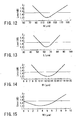
- FIG. 12 shows a change of loss made when the distance G was changed.
- the target value 1.5 dB could be ensured.
- FIG. 13 shows a change of loss made when the length L was changed.
- the target value 1.5 dB could be ensured.
- the length L is in inverse proportion to the change of the relative refractive index difference ⁇ between the core layer 20 and the clad layer 21. If the relative refractive index difference ⁇ changes, therefore, the product of the length L ( ⁇ m) and the relative refractive index difference ⁇ is substantially fixed.
- the refractive index (nc 1 ) of the clad layer 21 is 1.4574
- the refractive index (nc 0 ) of the core layer 20 and each channel waveguide 25 is 1.4684, so that the relative refractive index difference ⁇ is 0.0075.
- the target value 1.5 dB can be ensured if the product (L ⁇ ⁇ ) of the length L ( ⁇ m) and the relative refractive index difference ⁇ ranges from 0.4 to 0.6.
- FIG. 14 shows a change of loss made when the width W1 of one end 30a of each tapered island region 30 was changed.
- the width W1 ranged from 9.5 ⁇ m to 15.5 ⁇ m, the target value 1.5 dB could be ensured.
- the array pitch of the channel waveguides 25 is 25 ⁇ m, the range from 9.5 ⁇ m to 15.5 ⁇ m is equivalent to 38% to 62% of the array pitch P.
- FIG. 15 shows a change of loss made when the width W2 of the other end 30b of each tapered island region 30 was changed.
- the width W2 ranged from 0 ⁇ m to 6.5 ⁇ m, the target value 1.5 dB could be ensured.
- the array pitch P of the channel waveguides 25 is 25 ⁇ m, the range from 0 ⁇ m to 6.5 ⁇ m is equivalent to 0% to 26% of the array pitch P. If W2 accounts for 0% of the pitch P, it implies that the other end 30b of the island region 30 is sharp-pointed like the vertex of an isosceles triangle.
- FIG. 16 shows a slab waveguide 13 and an arrayed waveguide 14 of an optical multiplexer/demultiplexer according to a fourth embodiment of the invention.
- the array pitch of island regions 30 and an array pitch P of channel waveguides 25 are slightly deviated from each other by ⁇ P.
- the difference between the pitch of axes C1 of the island regions 30 and the pitch P of the channel waveguides 25 at a connecting end 14a of the arrayed waveguide 14 is referred to as a chirping level ⁇ P.
- the array pitch P of the channel waveguides 25 and the chirping level ⁇ P are adjusted to 25 ⁇ m and 0.2 ⁇ m, respectively.
- the pitch of the island regions 30 is adjusted to 24.8 ⁇ m or 25.2 ⁇ m.
- each island region 30 and the axis of a region 35 between each two adjacent channel waveguides 25 and opposite the island region 30 are C1 and C2, respectively, as shown in FIG. 16.
- the island regions 30 are arranged at pitches (P - ⁇ P) such that the deviation between C1 and C2 gradually increases from a specific island region 30 1 toward the opposite side portions 13a and 13b (shown in FIG. 1) of the slab waveguide 13.
- the array pitch of the island regions 30 is smaller than the array pitch P of the channel waveguides 25 by ⁇ P.
- the axis C1 of an nth island region 30 as counted from the specific island region 30 1 is deviated from the axis C2 of the arrayed waveguide 14 by (n ⁇ ⁇ P).
- the specific island region 30 1 is an island region that is situated in the center of the input slab waveguide 13 with respect to the width direction, for example.
- the deviation (n ⁇ ⁇ P) between the axes C1 and C2 increases from the specific island region 30 1 toward the opposite side portions of the input slab waveguide 13.
- the field distribution (remote field) at the optical point of convergence is controlled by deviating the respective pitches of the island regions 30 and the channel waveguides 25 from each other in this manner. By doing this, those components of the optical power that influence crosstalk can be restrained satisfactorily.
- FIG. 17 shows the results of simulations in which changes of loss and crosstalk were obtained when the chirping level ⁇ P was changed.
- the number of channels was adjusted to 8, the slab waveguide radius to 9,381 ⁇ m, the number of channel waveguides to 60, and the pitch P of the channel waveguides to 25 ⁇ m.
- the respective length difference between each two adjacent channel waveguides is 126 ⁇ m.
- the wavelength interval is about 0.8 nm, which is equivalent to the frequency interval of 100 GHz.
- the crosstalk level falls with the increase of the chirping level, as shown in FIG. 17.
- the insertion loss somewhat increases as the crosstalk level lowers, it is only about 7 dB at the maximum. As compared with the level of the type without any island regions, therefore, this level is still low enough for practical use. The best result was obtained when the chirping level was at ⁇ 0.4 ⁇ m.
- FIG. 18 shows a slab waveguide 13 and an arrayed waveguide 14 of an optical multiplexer/demultiplexer according to a fifth embodiment of the invention.
- the width W1 of the one end 30a of each tapered island region 30 is gradually reduced by ⁇ W at a time from the center of the input slab waveguide 13 toward the opposite side portions.
- the width W2 of the other end 30b of each island region 30 is fixed.
- the fifth embodiment arranged in this manner can reduce the crosstalk level.
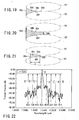
- FIG. 19 shows an island region 30A according to a sixth embodiment of the invention by hatching.
- Opposite side faces 30e and 30f of this island region 30A have a taper shape such that they individually extend along opposite half arcs of two adjacent ellipses V1 and V2.
- FIG. 20 shows an island region 30B according to a seventh embodiment of the invention.
- Opposite side faces 30e and 30f of this island region 30B have a taper shape such that they individually extend along opposite half arcs of two separate ellipses V1 and V2.
- FIG. 21 shows an island region 30C according to an eighth embodiment of the invention.
- a length L of this island region 30C is shorter than a half arc of each of ellipses V1 and V2 in the direction of the major axis thereof.
- island regions 30A, 30B and 30C having the side faces 30e and 30f that extend along the ellipses, light incident on the island regions 30A, 30B and 30C can be efficiently concentrated on the channel waveguides 25.
- the insertion loss and crosstalk can be reduced by increasing the number of channel waveguides of the arrayed waveguide and the number of island regions. This effect may be also obtained with use of the conventional arrayed-waveguide grating (AWG). With use of the structure of the present invention that has the island regions in the slab waveguide, in particular, however, the insertion loss and crosstalk can be reduced more effectively.
- AMG arrayed-waveguide grating
Landscapes
- Physics & Mathematics (AREA)
- General Physics & Mathematics (AREA)
- Optics & Photonics (AREA)
- Engineering & Computer Science (AREA)
- Microelectronics & Electronic Packaging (AREA)
- Optical Integrated Circuits (AREA)
- Diffracting Gratings Or Hologram Optical Elements (AREA)
Description
- The present invention relates to an optical multiplexer/demultiplexer used to multiplex or demultiplex wavelength division multiple signals, and more particularly, an optical multiplexer/demultiplexer capable of reducing insertion loss and crosstalk.
- In the field of optical communication, a wavelength division multiplexing transmission system is examined such that light beams of different wavelengths are loaded individually with a plurality of signals and information capacity is enlarged by transmitting the signals by means of one optical fiber. In this transmission system, optical multiplexer/demultiplexers for multiplexing or demultiplexing light beams of different wavelengths play an important role. Among various other optical multiplexer/demultiplexers, an optical multiplexer/demultiplexer that uses an arrayed-waveguide grating (AWG) holds promise, since it can increase the frequency of multiplexing with short wavelength intervals.
- In one such optical multiplexer/demultiplexer used in the wavelength division multiplexing transmission system, it is essential to reduce loss in a wavelength passband in consideration of the wavelength control tolerance of a semiconductor laser beam source, gain characteristics of an optical fiber amplifier, wavelength characteristics of a dispersion compensating fiber, etc. It is also important to ensure sharp rising and falling edges in the passband. Conventionally, there is a proposal to taper an end portion of an arrayed waveguide in order to reduce loss in the wavelength passband. Described in Jpn. Pat. Appln. KOKAI Publication No. 5-313029, for example, is an arrayed waveguide that has a tapered end portion on the interface between an input slab waveguide and the arrayed waveguide.
- According to this prior art structure in which the end portion of the arrayed waveguide is tapered, however, a loss is caused by the difference between the respective native modes of the slab waveguide and the arrayed waveguide, so that reduction of loss is limited.
- It is found that crosstalk can be reduced by maximizing the width of the slab waveguide and increasing the number of channel waveguides of the arrayed waveguide that are connected to the slab waveguide. If the channel waveguides of the arrayed waveguide are increased in number, however, they are easily influenced by the refractive index distribution and fluctuations of the channel waveguide width. This leads to adverse results including an increase in loss and a worsened crosstalk level.
- Crosstalks are calculated in the following manner.
- FIG. 22 shows a wavelength characteristic of a channel No. 5 out of eight channels of an AWG of 100 GHz as an example. The criterion for the calculation of crosstalks is not 0 (zero) dB but insertion loss for the center wavelength.
- For example, a in FIG. 22 indicates insertion loss for the center wavelength of the channel No. 5. Further, b indicates a crosstalk between channels No. 5 and No. 6; c, crosstalk between channels No. 5 and No. 4; d, crosstalk between channels No. 5 and No. 7; e, crosstalk between channels No. 5 and No. 8; f, crosstalk between channels No. 5 and No. 3; g, crosstalk between channels No. 5 and No. 2; and h, crosstalk between channels No. 5 and No. 1.
- The average of all the crosstalks in the channel No. 5 can be given by (b + c + d + e + f + g + h)/7. In this specification, the value calculated in this manner is referred to as crosstalk.
- As a power splitter for splitting signal light, on the other hand, a splitter that combines a slab waveguide and channel waveguides is proposed in place of a conventional splitter that is composed of multilayered Y-branches. "An integrated power splitter with ultra-low loss" (Integrated Photonics Research 1999, Santa Barbara, CA, July 19-21, 1999, pp. 141-143) is reported as an example of the proposed splitter. In this splitter, a semiconductor with a refractive index of 3.0 or more is used as its material, and a high-refraction region with a refractive index higher than that of a core layer is provided in the slab waveguide.
- Since this splitter uses a rib waveguide with a core width of 1 µm as its output waveguide, however, its mode diameter is as small as about 1 µm. Since the mode diameter of an ordinary optical fiber ranges from 9 to 10 µm, on the other hand, the mode mismatch (connection loss) in the output waveguide portion is substantial. It is feared that this difference in mode diameter should entail a loss of 13 dB or more. Thus, the loss of the whole splitter, including the splitter's own loss of 6 to 7 dB, inevitably amounts to about 20 dB, a substantial loss.
- In addition, the aforesaid high-refraction region in the slab waveguide measures only 2.5 µm by 0.9 µm. Thus, the individual parts have very fine dimensions, and the layer structure is complicated, so that the manufacture of the splitter is subject to variation. Thus, the quality of the splitter lacks stability and reproducibility. It is hard, therefore, to improve insertion loss or the like remarkably by means of a splitter of this type.
- M.R. Amersfoort, C.R. de Boer, F.P.G.M. van Ham, M.K. Smit, P.D. Demeester, J.J.G.M. van der Tol and A. Kuntze: "Phased-array wavelength demultiplexer with flattened wavelength response", in: Electronics Letters, IEE Tevenage. GB, Vol. 30, No. 4, 17 February 1994, pages 300 to 302 discloses an optical phased-array wavelength demultiplexer comprising wide multimode output waveguides in order to flatten the spectral response of the demultiplexer.
- The
US-Patent 5,745,618 discloses an optical multiplexer/demultiplexer comprising a slab waveguide and a separate transition region. The transition region is structured of array waveguides, and silica paths which intersect the array waveguides. As the silica path intersect the array waveguides, the transition region is formed in a lattice pattern. The length of the slab waveguide is determined according to the optical property of the slab waveguide and a boundary lies between the slab waveguide and the array waveguides. The transition region as formed in the region of the array waveguides beyond this boundary. The transition region lies outside of the slab waveguide. - The object of the present invention is to provide an optical multiplexer/demultiplexer enjoying lowered coupling loss and improved crosstalk that is easy to manufacture.
- An optical multiplexer/demultiplexer of the present invention comprises an input waveguide to which wavelength division multiple signals are applied; a plurality of output waveguides for demultiplexing and outputting the wavelength division multiple signals; an arrayed waveguide provided between the input waveguide and the output waveguides and including a plurality of channel waveguide having different waveguide lengths; an input slab waveguide formed between the input waveguide and the arrayed waveguide, said input slab waveguide (13) including a core layer (20) and a clad layer (21) and having axes (x) extending from the input waveguides (12) to the channel; an output slab waveguide formed between the arrayed waveguide and the output waveguides, said output slab waveguide (15) including a core layer (20) and a clad layer (21) and having axes (x) extending from the output waveguide (16) to the channel waveguides (25); and two or more island regions having a refractive index different from that of core layers of the input and output slab waveguides, providing in at least one of the slab waveguides, and situated in positions associated with the channel waveguides of the arrayed waveguide being elongated and extending along one of said axes.
- According to this invention, the island regions are formed in the slab waveguide, whereby field distribution at the end point of the input slab waveguide can be approximated to field distribution in the arrayed waveguide, so that a low-loss version of the optical multiplexer/demultiplexer can be obtained.
- In the present invention, the refractive index of the island regions is lower than that of the core layer around the island regions, for example. According to this invention, light that passes through the island regions can be concentrated on the channel waveguides of the arrayed waveguide.
- Preferably, in the present invention, the island regions are formed integrally with a clad layer of the slab waveguide. According to this invention, the refractive index of the island regions can be made equal to that of the clad layer. In designing mask patterns in the process of manufacturing the optical multiplexer/demultiplexer, therefore, the island regions can be formed integrally with the clad layer in a given position in the slab waveguide by only forming patterns corresponding to the island regions. Thus, there is no necessity of changing or adding manufacturing processes despite the presence of the island regions.
- In the case where the refractive index of the island regions is lower than that of the core layer around the island regions, the island regions are preferably located between axes connecting the input waveguide or the output waveguides and the channel waveguides of the arrayed waveguide. According to this invention, the island regions are provided individually between the axes that connect the input waveguide or output waveguides and the channel waveguides of the arrayed waveguide, so that the light that passes through the island regions can be concentrated on the channel waveguides of the arrayed waveguide.
- In the case where the refractive index of the island regions is higher than that of the core layer around the island regions, a desired result may possibly be obtained by forming the island regions on the axes individually.
- Preferably, in the present invention, each of the island regions is tapered so that the width thereof decreases toward the arrayed waveguide. If the island regions are tapered in this manner, the intensity distribution in the slab waveguide can be controlled, so that the efficiency of coupling to the arrayed waveguide can be improved. According to this invention, the degree of concentration of light on the channel waveguides of the arrayed waveguide can be further improved.
- Preferably, in the present invention, the width of that end of each of the island regions which faces the arrayed waveguide is 5 µm or more and is shorter than the pitch of the channel waveguides of the arrayed waveguide. Thus, etching can be easily carried out in forming the slab waveguides, arrayed waveguide, input waveguide, and output waveguides, and the quality can be securely stabilized. In forming the clad layer, moreover, the clad layer can be securely embedded in the core layer and the island regions with good capability.
- In the present invention, the width and/or pitch of each of the island regions should vary with regard to distance from the center of the slab waveguide toward the side portions of the slab waveguide, in some cases. For example, the respective widths of the island regions are gradually reduced from the center of the slab waveguide toward the side portions thereof. By gradually changing the respective shapes of the island regions, according to this invention, generation of side lobes can be restrained, and the crosstalk properties can be further improved.
- In the present invention, a value Q can be minimized so that there is a relation N × H < 40,000 × (logQ)-5, where N is the number of channels for the wavelength division multiple signals applied to the input waveguide, H (GHz) is the frequency interval, and Q is the number of channel waveguides of the arrayed waveguide. According to this invention, the array pitch of the arrayed waveguide can be widened, and the number of channel waveguides can be reduced.
- Preferably, in the present invention, the width of the wider end of each of the tapered island regions accounts for 38% to 62% of the array pitch of the channel waveguides, the width of the narrower end accounts for 0% to 26% of the array pitch of the channel waveguides, the product of the length of the island region and the relative refractive index difference ranges from 0.4 to 0.6, and the distance from the island region and the connecting end of the arrayed waveguide ranges from 100 µm to 150 µm. According to this invention, loss and crosstalk can be further lowered by optimizing the respective dimensions or lengths of the opposite ends of the tapered island regions or the relative positions of the island regions and the arrayed waveguide.
- Preferably, in the present invention, the array pitch of the island regions is different from the array pitch of the channel waveguides. If the array pitch of the channel waveguides is 25 µm, for example, the array pitch of the island regions is adjusted to 24.8 µm or 25.2 µm. According to this invention, field distribution at the focal point can be changed into one with a low crosstalk by slightly deviating the respective array pitches of the island regions and the channel waveguides from each other.
- Preferably, in the present invention, deviations between the respective axes of the island regions and the respective axes of regions opposite the island regions and between the channel waveguides gradually increase with distance from a specific island region or as the side portions of the slab waveguide are approached. According to this invention, the field distribution at the focal point can be changed into a desired one by changing the deviation between the island regions and the channel waveguides in the direction of arrangement of the island regions.
- In this specification and the accompanying drawings, insular regions of the present invention or "regions formed in the slab waveguide and having a refractive index different from that of the core layer of the slab waveguide" are referred to as "island regions" or simply as "islands" in some cases.
- This summary of the invention does not necessarily describe all necessary features so that the invention may also be a sub-combination of these described features.
- The invention can be more fully understood from the following detailed description when taken in conjunction with the accompanying drawings, in which:
- FIG. 1 is a plan view of a part of an optical multiplexer/demultiplexer according to an embodiment of the invention;
- FIG. 2 is a general perspective view of the optical multiplexer/demultiplexer shown in FIG. 1;
- FIG. 3 is a sectional view of a part of the optical multiplexer/demultiplexer taken along line F3-F3 of FIG. 1; .
- FIG. 4 is a sectional view of a part of the optical multiplexer/demultiplexer taken along line F4-F4 of FIG. 1;
- FIG. 5 is an enlarged view showing the principal part of the optical multiplexer/demultiplexer shown in FIG. 1;
- FIG. 6 is a plan view of an island region of the optical multiplexer/demultiplexer shown in FIG. 1;
- FIG. 7 is a plan view of an island region of an optical multiplexer/demultiplexer according to a second embodiment of the invention;
- FIG. 8 is a sectional view of a part of an optical multiplexer/demultiplexer according to a third embodiment of the invention;
- FIG. 9 is a sectional view of an island region of the optical multiplexer/demultiplexer shown in FIG. 8;
- FIG. 10 is a diagram showing the respective outputs of the optical multiplexer/demultiplexers of the first and second embodiments and a conventional optical multiplexer/demultiplexer
- FIG. 11 is a diagram showing the relationship between the number of channel waveguides and the product of the number of signal beam channels and the frequency interval;
- FIG. 12 is a diagram showing the relationship between loss and a distance G between the island region and an arrayed waveguide shown in FIG. 6;
- FIG. 13 is a diagram showing the relationship between loss and a length L of the island region shown in FIG. 6;
- FIG. 14 is a diagram showing the relationship between loss and a width W1 of one end of the island region shown in FIG. 6;
- FIG. 15 is a diagram showing the relationship between loss and a width W2 of the other end of the island region shown in FIG. 6;
- FIG. 16 is a plan view of a part of an optical multiplexer/demultiplexer according to a fourth embodiment of the invention;
- FIG. 17 is a diagram showing relationships between the chirping level of island regions shown in FIG. 16, loss, and crosstalk;
- FIG. 18 is a plan view of a part of an optical multiplexer/demultiplexer according to a fifth embodiment of the invention;
- FIG. 19 is a plan view showing an island region according to a sixth embodiment of the invention by hatching;
- FIG. 20 is a plan view showing an island region according to a seventh embodiment of the invention by hatching;
- FIG. 21 is a plan view showing an island region according to an eighth embodiment of the invention by hatching; and
- FIG. 22 is a wavelength characteristic curve for illustrating crosstalk.
- A first embodiment of the present invention will now be described with reference to FIGS. 1 to 6.
- FIG. 2 shows a waveguide-type wavelength multiplexing multiplexer/demultiplexer element (hereinafter referred to as optical multiplexer/demultiplexer 10) that uses an arrayed-waveguide grating.
- The optical multiplexer/demultiplexer a
substrate 11 formed of silica glass or silicon, for example, a plurality ofinput waveguides 12, aninput slab waveguide 13, an arrayedwaveguide 14, anoutput slab waveguide 15, a plurality ofoutput waveguides 16, etc. Optical fibers (not shown) are connected optically to theinput waveguides 12, which receive wavelength division multiple signals through the optical fibers. - As shown in FIG. 3, the
input slab waveguide 13 is provided with thesubstrate 11 of silica glass, acore layer 20 spread flat on thesubstrate 11, and aclad layer 21 covering thecore layer 20. Theinput slab waveguide 13 is formed between theinput waveguides 12 and the arrayedwaveguide 14, and optically connects thewaveguides input waveguides 12 to theinput slab waveguide 13 are spread in thecore layer 20 of thewaveguide 13 by a diffraction effect, and land onchannel waveguides 25 of the arrayedwaveguide 14. - The arrayed
waveguide 14 includes a plurality ofchannel waveguides 25. The respective lengths of each twoadjacent channel waveguides 25 are somewhat different. Therefore, the wavelength division multiple signals delivered from the one end of thechannel waveguides 25 undergoes an optical phase shift for each frequency as they propagate to the other end of thechannel waveguides 25. This phase shift depends on the wavelength of light, and the wave front of converged light is inclined according to the wavelength. Thus, the respective positions of convergence of light beams in theoutput slab waveguide 15 vary depending on the respective wavelengths of the beams. - The light beams with different wavelengths demultiplexed in this manner are fetched individually from
separate output waveguides 16 according to the wavelengths. Thus, theoutput slab waveguide 15 is formed between the arrayedwaveguide 14 and theoutput waveguides 16. Thewaveguide 15 optically connects thewaveguides output slab waveguide 15 may be constructed substantially in the same manner as theinput slab waveguide 13. - For convenience, in this specification, the waveguides (e.g., waveguides 12) on the incidence side are referred to as input waveguides, and the waveguides (e.g., waveguides 16) on the emission side as output waveguides. If the light is incident in the opposite direction, however, the
waveguides 12 serve as the output waveguides, and thewaveguides 16 as the input waveguides. Thus, the optical multiplexer/demultiplexer 10 can fulfill equal functions with respect to either direction of signal light transmission. - The optical multiplexer/
demultiplexer 10 is provided with two or more island regions 30 (typically shown in FIG. 1) in theinput slab waveguide 13 and/or theoutput slab waveguide 15. Theregions 30 have a refractive index different from that of thecore layer 20 of theslab waveguide input waveguides 12. - In the case of this embodiment, the refractive index of the
island regions 30 is lower than that of thecore layer 20 that surrounds theregions 30. As shown in FIG. 4, theisland regions 30 are formed on thesubstrate 11 formed of silica glass or the like, and preferably, formed integrally with the cladlayer 21 of theinput slab waveguide 13. - The
island regions 30 are formed in positions that are associated with thechannel waveguides 25 of the arrayedwaveguide 14, individually. More specifically, if the refractive index of theisland regions 30 is lower than that of thecore layer 20, theisland regions 30 are formed individually between axes X that connect eachinput waveguide 12 and thechannel waveguides 25 of the arrayedwaveguide 14, as shown in FIG. 1. - These
island regions 30 are arranged at spaces from the center of theinput slab waveguide 13 towardopposite side portions island regions 30 of this embodiment are formed so that the distance from eachchannel waveguide 25 of the arrayedwaveguide 14 is fixed. The number ofisland regions 30 is one more than the number ofchannel waveguides 25. - If the
island regions 30 are tapered, as in the case of this embodiment, the optical power distribution in theinput slab waveguide 13 can be more easily coupled to thechannel waveguides 25 of the arrayedwaveguide 14, as mentioned later. Thus, the optical power can be efficiently concentrated on the arrayedwaveguide 14 even if each array pitch P (shown in FIG. 1) of thechannel waveguides 25 is widened to about 30 µm or more, for example. If thechannel waveguides 25 are reduced in number, therefore, loss in th.e optical multiplexer/demultiplexer 10 as a whole cannot be increased, and crosstalk cannot be worsened. - As shown in the enlarged views of FIGS. 5 and 6, each
island region 30 of this embodiment is tapered (in the shape of an elongate trapezoid) so that a width W1 of oneend 30a, as viewed toward the arrayedwaveguide 14, is greater than a width W2 of theother end 30b. The width W2 of thatend 30b of eachisland region 30 which faces the arrayedwaveguide 14 is 5 µm or more and is shorter than the pitch P of thechannel waveguides 25. A length L of eachisland region 30 ranges from 50 µm to 100 µm, for example. - FIG. 7 shows an island region 30' according to a second embodiment of the present invention. The island region 30' has a substantially fixed width W3 (or is rectangular) throughout its length from one end to the other. Since the island region 30' shares other configurations with those of the optical multiplex/
demultiplexer 10 of the first embodiment, a description of those configurations is omitted. - The following is a description of a manufacturing method for the optical multiplexer/
demultiplexer 10 of the first embodiment. - Silica glass is used for the
substrate 11. The respective core layers 20 of theslab waveguides channel waveguides 25 of the arrayedwaveguide 14 are integrally formed of silica glass doped with germanium and have a thickness of 6 µm. The glass material may be formed by the chemical vapor deposition (CVD), flame deposition (FHD), or vapor deposition. The refractive index (nc1) of the cladlayer 21 was adjusted to nc1 = 1.4574, the refractive index (nc0) of thecore layer 20 and eachchannel waveguide 25 to nc0 = 1.4684, the relative refractive index difference to Δ = 0.75%, and the sectional area of eachchannel waveguide 25 to 6 × 6 µm2. - The respective patterns of the
core layer 20 and theisland regions 30 were simultaneously formed by reactive ion etching. After the patterns were formed, the cladlayer 21 was formed into a given thickness. Eachisland region 30 of this embodiment is formed by partially scooping thecore layer 20 and filling the resulting hollow with a part of the cladlayer 21. In aslab waveguide 13 of an optical multiplexer/demultiplexer according to a third embodiment shown in FIGS. 8 and 9, silicon is used for asubstrate 11. In theslab waveguide 13, a lower clad layer 21' is formed between thesubstrate 11 and acore layer 20. - The following is a description of the operation of the optical multiplexer/
demumtiplexer 10. - Wavelength division multiple signal beams from the
input waveguides 12 incident on theinput slab waveguide 13 spread in thewaveguide 13 in the width direction thereof. In FIG. 5, PH1 designates a wavefront of the incident signal beams. Among the spread signal beams, beams A1 that are directed toward thechannel waveguides 25 of the arrayedwaveguide 14 without passing through theisland regions 30 advance straight along the axes X and land on thechannel waveguides 25, individually. - Among the light beams from the
input waveguides 12 incident on theinput slab waveguide 13, some beams A2 reach theisland regions 30, individually. If the refractive index of theisland regions 30 is lower than that of thecore layer 20, the beams A2 that pass through theisland regions 30 tend to have their phases advance faster than those of the beams A1 that never pass through theisland regions 30. Accordingly, the wavefront is deformed as indicated by PH2, so that the advancing direction of the beams A2 is slightly inclined. - The shape and position of each
island region 30 are optimized so that the inclination of the advancing direction of the beams A2 is directed toward thechannel waveguides 25 of the arrayedwaveguide 14. By doing this, the beams A2 can be concentrated on thechannel waveguides 25 of the arrayedwaveguide 14. Thus, light beams that leak to the cladlayer 21 from between thechannel waveguides 25 are reduced, so that coupling loss from theinput slab waveguide 13 to the arrayedwaveguide 14 lessens. - In the case of a conventional optical multiplexer/demultiplexer that is not provided with the
island regions 30, some of light beams from input waveguides incident on an input slab waveguide leak to a clad layer from between channel waveguides. The beams leaked to the clad layer are in a radiation mode, not in a guided mode, and most of them are lost. Some of these radiated beams may reach an output slab waveguide, in some cases. Since their phases are not controlled at all, these beams cause noise in the output slab waveguide and worsen crosstalk. - The inventors hereof conducted a simulation to couple light from the
input slab waveguide 13 to the arrayedwaveguide 14. In this simulation, the conventional structure (without the island regions 30) and the structures of the foregoing embodiments having theisland regions 30 were checked for variation in coupling loss. FIG. 10 shows the result of this simulation. - As conditions for this simulation, the refractive index (nc1) of the clad
layer 21 was adjusted to nc1 = 1.4574, the refractive index (nc0) of thecore layer 20 and eachchannel waveguide 25 to nc0 = 1.4692, the relative refractive index difference to Δ = 0.75%, the sectional area of eachchannel waveguide 25 to 6 × 6 µm2, the slab waveguide radius to R = 2,380 µm, and the demultiplexing interval to 705 GHz in terms of frequency (Δ λ = 5.64 nm in terms of wavelength) - The simulation indicated that the loss of the conventional structure was 4 dB. It was confirmed, on the other hand, that the loss could be reduced to 0.34 dB according to the first embodiment of the invention (provided with the tapered
island regions 30 shown in FIG. 6). It was confirmed, moreover, that the loss could be reduced to 1.2 dB according to the second embodiment of the invention (provided with the rectangular island regions 30' shown in FIG. 7). - The respective lengths of each two adjacent ones of the
channel waveguides 25 that constitute the arrayedwaveguide 14 are somewhat different. Therefore, the wavelength division multiple signals applied to the arrayedwaveguide 14 undergoes an optical phase shift for each frequency as they propagate from thechannel waveguide 25 to theoutput slab waveguide 15. As this is done, wavelength multiplexing signal beams are focused on different points according to the wavelength. In consequence, light beams having their respective wavelengths are dividedly incident on theoutput waveguides 16. - The
island regions 30 may possibly be provided on both in input andoutput slab waveguides slab waveguides demultiplexer 10 of each of the foregoing embodiments). - In the case where the
island regions 30 are not formed in theoutput slab waveguide 15, for example, theslab waveguide 15 is shorter than in the case where theisland regions 30 are not formed. This is because the point of convergence is settled when light from the arrayedwaveguide 14 reaches theoutput slab waveguide 15. If theisland regions 30 are formed in theoutput slab waveguide 15, light is influenced again by phase change as it pass through theisland regions 30. In this case, therefore, the distance from the point of convergence is settled when the passage through theisland regions 30 is finished. - By successively changing the width of the
island regions 30 from the center of theinput slab waveguide 13 toward the opposite side portions, for example, generation of side lobes can be restrained, and the crosstalk properties can be further improved. In the case where all theisland regions 30 have the same shape, positions that meet the conditions for the generation of side lobes approach the main lobe, so that leakage of light to output waveguides other than a specific one tends to increase. - By gradually changing the respective shapes of the
island regions 30, therefore, the positions that meet the conditions for the generation of the side lobes can be kept wide apart from the main lobe. Thus, light beams that are incident on output waveguides other than the specific one can be reduced. - The inventors hereof conducted a simulation to analyze the wavelength characteristics of the conventional optical multiplexer/demultiplexer without the
island regions 30, thereby obtaining insertion loss and crosstalk values. In consequence, the minimum insertion loss and the crosstalk level of any other channels than adjacent ones were found to be -4.46 dB and 41.38 dB, respectively. The number (N) of channels for the signal beams was adjusted to 8, the refractive index (nc1) of the clad layer to nc1 = 1.4574, the refractive index (nc0) of the core layer to nc0 = 1.4692, the relative refractive index difference to Δ = 0.75%, the sectional area of each channel waveguide to 6 × 6 µm2, the slab waveguide radius to R = 2,380 µm, and the demultiplexing interval to 705 GHz in terms of frequency (Δλ = 5.64 nm in terms of wavelength). - In the case of the optical multiplexer/
damultiplexer 10 of each of the foregoing embodiments in which a plurality ofisland regions 30 with the same shape are situated in equivalent positions with respect to the directions of the respective axes X of the slab waveguides, on the other hand, the insertion loss and the crosstalk were found to be -1.81 dB and 41.39 dB, respectively. Thus, it was confirmed that the insertion loss of the optical multiplexer/demultiplexer 10 was about 2.7 dB better than that of the conventional example. - The inventors hereof also conducted a simulation for an embodiment such that the respective positions of the
island regions 30 with the same shape are gradually varied with respect to the directions of the respective axes X of the slab waveguides. In this embodiment, the insertion loss and the crosstalk were found to be -3.27 dB and 50.45 dB, respectively. Thus, it was confirmed that the crosstalk value of this embodiment was about 10 dB better than that of the conventional example without theisland regions 30. - Further, the inventors hereof examined the relation between the channel waveguide number Q of the arrayed
waveguide 14 and the product of the signal beam channel number N and the frequency interval H. FIG. 11 is a graph obtained by plotting the relation. In the case provided with theisland regions 30, there are plots inside a curved border line N × H = 40,000 × (logQ)-5. In the conventional case without theisland regions 30, on the other hand, plots were found to exist outside the curved border line. - Thus, in the case of the conventional optical multiplexer/demultiplexer without the
island regions 30, the number ofchannel waveguides 25 tends to increase if the channel number N and the frequency interval H are fixed. This is unavoidable in view of design for the achievement of a given insertion loss and the improvement of crosstalk. In the optical multiplexer/demultiplexer 10 according to each of the embodiments of the invention, on the other hand, theisland regions 30 are formed in at least one of theslab waveguides waveguide 14, so that the number ofchannel waveguides 25 can be made smaller than in the conventional case. - In each of the tapered
island regions 30 shown in FIGS. 1 and 6, the width of thewider end 30a is indicated by W1, the width of the other ornarrower end 30b by W2, the length of eachisland region 30 by L, the array pitch of thechannel waveguides 25 by P, and the distance from theother end 30b of eachisland region 30 to a connectingend 14a of the arrayedwaveguide 14 by G. In order to discriminate a target loss criterion from the loss of the conventional arrayed-waveguide grating (AWG), according to the present embodiment, it is adjusted to 1.5 dB, a practical smaller value. The array pitch P of thechannel waveguides 25 is 25 µm. - FIG. 12 shows a change of loss made when the distance G was changed. When the distance G ranged from 100 µm to 150 µm, the target value 1.5 dB could be ensured.
- FIG. 13 shows a change of loss made when the length L was changed. When the length L ranged from 55 µm to 75 µm, the target value 1.5 dB could be ensured. The length L is in inverse proportion to the change of the relative refractive index difference Δ between the
core layer 20 and theclad layer 21. If the relative refractive index difference Δ changes, therefore, the product of the length L (µm) and the relative refractive index difference Δ is substantially fixed. - In this embodiment, for example, the refractive index (nc1) of the clad
layer 21 is 1.4574, and the refractive index (nc0) of thecore layer 20 and eachchannel waveguide 25 is 1.4684, so that the relative refractive index difference Δ is 0.0075. In the case where the relative refractive index difference Δ is adjusted to 0.0075, the target value 1.5 dB can be ensured if the product (L × Δ) of the length L (µm) and the relative refractive index difference Δ ranges from 0.4 to 0.6. - FIG. 14 shows a change of loss made when the width W1 of one
end 30a of each taperedisland region 30 was changed. When the width W1 ranged from 9.5 µm to 15.5 µm, the target value 1.5 dB could be ensured. Since the array pitch of thechannel waveguides 25 is 25 µm, the range from 9.5 µm to 15.5 µm is equivalent to 38% to 62% of the array pitch P. - FIG. 15 shows a change of loss made when the width W2 of the
other end 30b of each taperedisland region 30 was changed. When the width W2 ranged from 0 µm to 6.5 µm, the target value 1.5 dB could be ensured. Since the array pitch P of thechannel waveguides 25 is 25 µm, the range from 0 µm to 6.5 µm is equivalent to 0% to 26% of the array pitch P. If W2 accounts for 0% of the pitch P, it implies that theother end 30b of theisland region 30 is sharp-pointed like the vertex of an isosceles triangle. - For these reasons, it is advisable to adjust the width W1 to 38% to 62% of the array pitch P, the width W2 to 0% to 26% of the array pitch P, the product of the length L (µm) and the relative refractive index difference Δ to 0.4 to 0.6, and the distance G from the
other end 30b of eachisland region 30 to the connectingend 14a of the arrayedwaveguide 14 to 100 µm to 150 µm. - FIG. 16 shows a
slab waveguide 13 and an arrayedwaveguide 14 of an optical multiplexer/demultiplexer according to a fourth embodiment of the invention. In order to improve crosstalk, in this embodiment, the array pitch ofisland regions 30 and an array pitch P ofchannel waveguides 25 are slightly deviated from each other by δP. In this specification, the difference between the pitch of axes C1 of theisland regions 30 and the pitch P of thechannel waveguides 25 at a connectingend 14a of the arrayedwaveguide 14 is referred to as a chirping level δP. - For example, the array pitch P of the
channel waveguides 25 and the chirping level δP are adjusted to 25 µm and 0.2 µm, respectively. In this case, the pitch of theisland regions 30 is adjusted to 24.8 µm or 25.2 µm. - More specifically, let it be supposed that the axis of each
island region 30 and the axis of aregion 35 between each twoadjacent channel waveguides 25 and opposite theisland region 30 are C1 and C2, respectively, as shown in FIG. 16. In this case, theisland regions 30 are arranged at pitches (P - δP) such that the deviation between C1 and C2 gradually increases from aspecific island region 301 toward theopposite side portions slab waveguide 13. Thus, the array pitch of theisland regions 30 is smaller than the array pitch P of thechannel waveguides 25 by δP. - Accordingly, the axis C1 of an
nth island region 30 as counted from thespecific island region 301 is deviated from the axis C2 of the arrayedwaveguide 14 by (n × δP). Thespecific island region 301 is an island region that is situated in the center of theinput slab waveguide 13 with respect to the width direction, for example. In this case, the deviation (n × δP) between the axes C1 and C2 increases from thespecific island region 301 toward the opposite side portions of theinput slab waveguide 13. - The field distribution (remote field) at the optical point of convergence is controlled by deviating the respective pitches of the
island regions 30 and thechannel waveguides 25 from each other in this manner. By doing this, those components of the optical power that influence crosstalk can be restrained satisfactorily. - FIG. 17 shows the results of simulations in which changes of loss and crosstalk were obtained when the chirping level δP was changed. The number of channels was adjusted to 8, the slab waveguide radius to 9,381 µm, the number of channel waveguides to 60, and the pitch P of the channel waveguides to 25 µm. The respective length difference between each two adjacent channel waveguides is 126 µm. In this configuration, the wavelength interval is about 0.8 nm, which is equivalent to the frequency interval of 100 GHz. It was confirmed that the crosstalk level falls with the increase of the chirping level, as shown in FIG. 17. Although the insertion loss somewhat increases as the crosstalk level lowers, it is only about 7 dB at the maximum. As compared with the level of the type without any island regions, therefore, this level is still low enough for practical use. The best result was obtained when the chirping level was at ±0.4 µm.
- FIG. 18 shows a
slab waveguide 13 and an arrayedwaveguide 14 of an optical multiplexer/demultiplexer according to a fifth embodiment of the invention. In order to improve crosstalk, in this embodiment, the width W1 of the oneend 30a of each taperedisland region 30 is gradually reduced by δW at a time from the center of theinput slab waveguide 13 toward the opposite side portions. The width W2 of theother end 30b of eachisland region 30 is fixed. The fifth embodiment arranged in this manner, like the fourth embodiment, can reduce the crosstalk level. - FIG. 19 shows an
island region 30A according to a sixth embodiment of the invention by hatching. Opposite side faces 30e and 30f of thisisland region 30A have a taper shape such that they individually extend along opposite half arcs of two adjacent ellipses V1 and V2. - FIG. 20 shows an
island region 30B according to a seventh embodiment of the invention. Opposite side faces 30e and 30f of thisisland region 30B have a taper shape such that they individually extend along opposite half arcs of two separate ellipses V1 and V2. - FIG. 21 shows an island region 30C according to an eighth embodiment of the invention. A length L of this island region 30C is shorter than a half arc of each of ellipses V1 and V2 in the direction of the major axis thereof.
- With use of the
island regions island regions channel waveguides 25. - According to the present invention, the insertion loss and crosstalk can be reduced by increasing the number of channel waveguides of the arrayed waveguide and the number of island regions. This effect may be also obtained with use of the conventional arrayed-waveguide grating (AWG). With use of the structure of the present invention that has the island regions in the slab waveguide, in particular, however, the insertion loss and crosstalk can be reduced more effectively.
Claims (10)
- An optical multiplexer/demultiplexer comprising:an input waveguide (12) to which wavelength division multiple signals are applied; a plurality of output waveguides (16) for demultiplexing and outputting the wavelength division multiple signals;an arrayed waveguide (14) provided between the input waveguide (12) and the output waveguides (16) and including a plurality of channel waveguides (25) having different waveguides lengths;an input slab waveguide (13) formed between the input waveguide (12) and the arrayed waveguide (14), said input slab waveguide (13) including a core layer (20) and a clad layer (21); and having axes (x) extending from the input waveguide (12) to the channel waveguides (25);an output slab waveguide (15) formed between the arrayed waveguide (14) and the output waveguides (16), said output slab waveguide (15) including a core layer (20) and a clad layer (21) and having axes (x) extending from the output waveguide (16) to the channel waveguides (25),andtwo or more island regions (30) having a refractive index different from that of the core layers (20) of the input and output slab waveguides (13, 15), provided in at least one of the slab waveguides (13, 15) and situated in positions associated witch the channel waveguides (25) of the arrayed waveguide (14) being elongated and extending along one of said axes (x),characterized in that each said island region (30) is tapered so that the width thereof decreases toward the arrayed waveguide (14).
- An optical multiplexer/demultiplexer according to claim 1, characterized in that the refractive index of said island regions (30) is lower than that of the core layer (20) around the island regions (30).
- An optical multiplexer/demultiplexer according to claim 2, characterized in that said island regions (30) are formed integrally with the clad layer (21) of the slab waveguide (13, 15).
- An optical multiplexer/demultiplexer according to claim 2, characterized in that said island regions (30) are formed between axes connecting the input waveguide (12) or the output waveguide (16) and the channel waveguides (25) of the arrayed waveguide (14).
- An optical multiplexer/demultiplexer according to claim 1, characterized in that the width (W2) of that end of each said island region (30) which faces the arrayed waveguide (14) is 5 µm or more and is shorter than a pitch of the channel waveguides (25) of the arrayed waveguide (14).
- An optical multiplexer/demultiplexer according to claim 1, characterized in that the width (W1) and/or pitch (p-δp) of each said island region (30) differs from the width (W) and/or pitch (p-δp) of the other island regions (30) with regard to distance from the center of the slab waveguide (13) toward the side portions (13a, 13b) of the slab waveguide (13).
- An optical multiplexer/demultiplexer according to claim 1, characterized in that there is a relation N x H < 40,000 x (logQ)-5, where N is the number of channels for the wavelength division multiple signals applied to the input waveguide (12), H (GHz) is the frequency interval, and Q is the number of channel waveguides (25) of the arrayed waveguide (14).
- An optical multiplexer/demultiplexer according to claim 1, characterized in that the width (W1) of wider end (30a) of each said tapered island region (30) accounts for 38% to 62% of the array pith (P) of the channel waveguides (25), the width (W2) of narrower end (30b) accounts for 0% to 26% of the array pitch (P) of the channel waveguides (25), the product of the length (L) of the island region (30) and the relative refractive index difference range from 0.4 to 0.6, and the distance (G) from the island region (30) and the connecting end (14a) of the arrayed waveguide (14) ranges from 100 µm to 150 µm.
- An optical multiplexer/demultiplexer according to claim 1, characterized in that an array pitch of said island regions (30) is different from an array pitch (P) of said channel waveguides (25), and a deviation (δPn) between the axis (C1) of each island region (30) and an axis (C2) passing between two channel waveguides (25) that oppose said each island region (30) is smaller than a next deviation (δPn+1) between an axis (C1) of the next outer island region (30) and an axis (C2) passing between two channel waveguides (25) that oppose the next outer island region (30).
- An optical multiplexer/demultiplexer according to claim 6, characterized in that an array pitch of said island regions (30) is different from an array pitch (P) of said channel waveguides (25), and a deviation (δPn) between axis (C1) of each island region (30) and an axis (C2) passing between two channel waveguides (25) that oppose said each island region (30) is smaller than a next deviation (δPn+1) between an axis (C1) of the next outer island region (30) and an axis (C2) passing between two channel waveguides (25) that oppose the next outer island region 30).
Applications Claiming Priority (4)
| Application Number | Priority Date | Filing Date | Title |
|---|---|---|---|
| JP2001128130 | 2001-04-25 | ||
| JP2001128130 | 2001-04-25 | ||
| JP2002007698 | 2002-01-16 | ||
| JP2002007698A JP3726062B2 (en) | 2001-04-25 | 2002-01-16 | Optical multiplexer / demultiplexer |
Publications (3)
| Publication Number | Publication Date |
|---|---|
| EP1253449A2 EP1253449A2 (en) | 2002-10-30 |
| EP1253449A3 EP1253449A3 (en) | 2004-04-14 |
| EP1253449B1 true EP1253449B1 (en) | 2007-10-10 |
Family
ID=26614216
Family Applications (1)
| Application Number | Title | Priority Date | Filing Date |
|---|---|---|---|
| EP02009013A Expired - Lifetime EP1253449B1 (en) | 2001-04-25 | 2002-04-23 | Optical multiplexer/demultiplexer |
Country Status (4)
| Country | Link |
|---|---|
| US (1) | US6898349B2 (en) |
| EP (1) | EP1253449B1 (en) |
| JP (1) | JP3726062B2 (en) |
| DE (1) | DE60222824T2 (en) |
Families Citing this family (21)
| Publication number | Priority date | Publication date | Assignee | Title |
|---|---|---|---|---|
| JP2003185865A (en) * | 2001-12-20 | 2003-07-03 | Fujitsu Ltd | Optical multiplexer / demultiplexer and waveguide type optical coupler |
| US7006729B2 (en) * | 2001-12-31 | 2006-02-28 | Wavesplitter Technologies, Inc. | Optical components having reduced insertion loss |
| JP3912250B2 (en) * | 2002-10-01 | 2007-05-09 | オムロン株式会社 | Optical multiplexer / demultiplexer |
| JP4150374B2 (en) * | 2003-02-26 | 2008-09-17 | 富士通株式会社 | Arrayed waveguide type wavelength multiplexer / demultiplexer |
| JP4626153B2 (en) * | 2004-02-20 | 2011-02-02 | 日本電気株式会社 | Manufacturing method of optical waveguide circuit |
| JP4069101B2 (en) * | 2004-07-01 | 2008-04-02 | 日本電信電話株式会社 | Waveguide type optical multiplexer / demultiplexer |
| JP4625420B2 (en) * | 2006-04-04 | 2011-02-02 | 日本電信電話株式会社 | Optical circuit |
| KR100968891B1 (en) | 2007-12-14 | 2010-07-09 | 한국전자통신연구원 | Wavelength Division Multiplexer / Demultiplexer with Flat Wavelength Response |
| US8086105B2 (en) | 2007-12-14 | 2011-12-27 | Electronics And Telecommunications Research Institute | Wavelength division multiplexer/demultiplexer having flat wavelength response |
| JP5327895B2 (en) * | 2010-05-27 | 2013-10-30 | Nttエレクトロニクス株式会社 | Optical waveguide and arrayed waveguide diffraction grating |
| JP5473868B2 (en) * | 2010-11-09 | 2014-04-16 | Nttエレクトロニクス株式会社 | Optical waveguide and arrayed waveguide diffraction grating |
| JP5327897B2 (en) * | 2010-12-22 | 2013-10-30 | Nttエレクトロニクス株式会社 | Optical waveguide and arrayed waveguide diffraction grating |
| JP5817147B2 (en) * | 2011-02-25 | 2015-11-18 | 国立大学法人九州大学 | Optical filter |
| KR101783621B1 (en) | 2011-09-09 | 2017-10-11 | 삼성전자주식회사 | Optical link, manufacturing method thereof and memory system having the same |
| US9116298B2 (en) * | 2013-03-15 | 2015-08-25 | Mitsubishi Electric Research Laboratories, Inc. | Multi-mode interference device |
| US9097852B2 (en) * | 2013-03-15 | 2015-08-04 | Mitsubishi Electric Research Laboratories, Inc. | Multi-mode interference device |
| US9164238B2 (en) * | 2013-09-16 | 2015-10-20 | Electronics And Telecommunications Research Institute | Optical coupler having self-focusing region and arryed-waveguide grating structure including the same |
| US10330863B2 (en) | 2017-04-18 | 2019-06-25 | Neophotonics Corporation | Planar lightwave circuit optical splitter / mixer |
| US10862610B1 (en) | 2019-11-11 | 2020-12-08 | X Development Llc | Multi-channel integrated photonic wavelength demultiplexer |
| US11187854B2 (en) * | 2019-11-15 | 2021-11-30 | X Development Llc | Two-channel integrated photonic wavelength demultiplexer |
| CN120447134A (en) * | 2024-02-06 | 2025-08-08 | 华为技术有限公司 | Optical chip structure, manufacturing method and wavelength division multiplexing system |
Family Cites Families (10)
| Publication number | Priority date | Publication date | Assignee | Title |
|---|---|---|---|---|
| JP3139571B2 (en) | 1992-05-13 | 2001-03-05 | 日本電信電話株式会社 | Optical multiplexer / demultiplexer |
| JP2870499B2 (en) * | 1996-08-02 | 1999-03-17 | 日立電線株式会社 | Optical wavelength multiplexer / demultiplexer |
| US5745618A (en) * | 1997-02-04 | 1998-04-28 | Lucent Technologies, Inc. | Optical device having low insertion loss |
| US6069990A (en) * | 1997-11-27 | 2000-05-30 | Hitachi Cable Ltd. | Optical wavelength multiplexer/demultiplexer |
| KR100274804B1 (en) * | 1998-04-22 | 2001-01-15 | 윤종용 | Bi-directional optical wavelength multiplexer and demultiplexer |
| KR100289052B1 (en) | 1998-11-17 | 2001-05-02 | 정선종 | Integrated optical coupler using phase-lattice structure |
| KR20000033948A (en) | 1998-11-26 | 2000-06-15 | 정선종 | Wavelength Multiple / Reverse Multiple Device without Diffraction Star Optical Coupler Coupling Loss |
| KR100322133B1 (en) * | 1999-02-01 | 2002-02-04 | 윤종용 | Optical multiplexer/demultiplexer having uniform loss |
| US6421478B1 (en) * | 1999-05-11 | 2002-07-16 | Jds Fitel Inc. | Tapered MMI coupler |
| US6665466B2 (en) * | 2000-09-05 | 2003-12-16 | Sumitomo Electric Industries, Ltd. | Optical multiplexer/demultiplexer |
-
2002
- 2002-01-16 JP JP2002007698A patent/JP3726062B2/en not_active Expired - Fee Related
- 2002-04-23 EP EP02009013A patent/EP1253449B1/en not_active Expired - Lifetime
- 2002-04-23 DE DE60222824T patent/DE60222824T2/en not_active Expired - Fee Related
- 2002-04-25 US US10/132,413 patent/US6898349B2/en not_active Expired - Fee Related
Also Published As
| Publication number | Publication date |
|---|---|
| EP1253449A3 (en) | 2004-04-14 |
| DE60222824T2 (en) | 2008-07-17 |
| US6898349B2 (en) | 2005-05-24 |
| JP3726062B2 (en) | 2005-12-14 |
| JP2003014962A (en) | 2003-01-15 |
| DE60222824D1 (en) | 2007-11-22 |
| US20020159696A1 (en) | 2002-10-31 |
| EP1253449A2 (en) | 2002-10-30 |
Similar Documents
| Publication | Publication Date | Title |
|---|---|---|
| US6898349B2 (en) | Optical multi-demultiplexer | |
| US6188818B1 (en) | Low loss AWG demultiplexer with flat spectral response | |
| US10663662B1 (en) | High density optical waveguide using hybrid spiral pattern | |
| US6888985B2 (en) | Arrayed waveguide grating and optical communication system using arrayed waveguide grating | |
| CA2315458C (en) | Optical wavelength multiplexer/demultiplexer | |
| JP4385224B2 (en) | Optical waveguide device and optical waveguide module | |
| US6195481B1 (en) | Array waveguide diffraction grating optical multiplexer/demultiplexer | |
| US20030012497A1 (en) | Dendritic taper for an integrated optical wavelength router | |
| US20020015559A1 (en) | Arrayed waveguide grating type optical multiplexer/demultiplexer and optical waveguide circuit | |
| US7106929B2 (en) | Waveguide device | |
| EP1219989A2 (en) | Arrayed waveguide grating type optical multiplexer/demultiplexer | |
| US6836591B2 (en) | Arrayed waveguide grating type optical multiplexer/demultiplexer and optical waveguide circuit | |
| US6741772B2 (en) | Optical multiplexer/demultiplexer and waveguide type optical coupler | |
| US6798952B2 (en) | Optical multiplexer/demultiplexer | |
| KR20110002619A (en) | Optical element | |
| US7031569B2 (en) | Optical multi-demultiplexer | |
| KR100851107B1 (en) | Optical waveguide device and transmission loss adjustment method | |
| JP3448518B2 (en) | Array waveguide diffraction grating | |
| US6728435B2 (en) | Arrayed waveguide grating type optical multiplexer/demultiplexer and optical waveguide circuit | |
| JP3224086B2 (en) | Arrayed waveguide grating with variable frequency width of flat band characteristics | |
| CA2409118C (en) | Optical multiplexer/demultiplexer | |
| EP1430342B1 (en) | Passband flattening in an arrayed waveguide grating | |
| US20020136492A1 (en) | Arrayed waveguide grating and method for manufacturing the same | |
| US6134361A (en) | Optical multiplexer/demultiplexer | |
| US20030086650A1 (en) | Arrayed waveguide grating type optical multiplexer/demultiplexer |
Legal Events
| Date | Code | Title | Description |
|---|---|---|---|
| PUAI | Public reference made under article 153(3) epc to a published international application that has entered the european phase |
Free format text: ORIGINAL CODE: 0009012 |
|
| 17P | Request for examination filed |
Effective date: 20020713 |
|
| AK | Designated contracting states |
Kind code of ref document: A2 Designated state(s): AT BE CH CY DE DK ES FI FR GB GR IE IT LI LU MC NL PT SE TR |
|
| AX | Request for extension of the european patent |
Free format text: AL;LT;LV;MK;RO;SI |
|
| RIN1 | Information on inventor provided before grant (corrected) |
Inventor name: MASUDA, MICHIYA Inventor name: YAMAUCHI, JUNJI Inventor name: NAKANO, HISAMATSU Inventor name: YAMAMOTO, YUICHI Inventor name: TAZAWA, RYOUICHI Inventor name: KAWAGUCHI, SHIGERU |
|
| PUAL | Search report despatched |
Free format text: ORIGINAL CODE: 0009013 |
|
| AK | Designated contracting states |
Kind code of ref document: A3 Designated state(s): AT BE CH CY DE DK ES FI FR GB GR IE IT LI LU MC NL PT SE TR |
|
| AX | Request for extension of the european patent |
Extension state: AL LT LV MK RO SI |
|
| RIC1 | Information provided on ipc code assigned before grant |
Ipc: 7G 02B 6/124 B Ipc: 7G 02B 6/293 A Ipc: 7G 02B 6/34 B |
|
| 17Q | First examination report despatched |
Effective date: 20040714 |
|
| AKX | Designation fees paid |
Designated state(s): DE FR GB IT |
|
| RAP1 | Party data changed (applicant data changed or rights of an application transferred) |
Owner name: OMRON CORPORATION |
|
| GRAP | Despatch of communication of intention to grant a patent |
Free format text: ORIGINAL CODE: EPIDOSNIGR1 |
|
| GRAS | Grant fee paid |
Free format text: ORIGINAL CODE: EPIDOSNIGR3 |
|
| GRAA | (expected) grant |
Free format text: ORIGINAL CODE: 0009210 |
|
| AK | Designated contracting states |
Kind code of ref document: B1 Designated state(s): DE FR GB IT |
|
| REG | Reference to a national code |
Ref country code: GB Ref legal event code: FG4D |
|
| REF | Corresponds to: |
Ref document number: 60222824 Country of ref document: DE Date of ref document: 20071122 Kind code of ref document: P |
|
| ET | Fr: translation filed | ||
| PLBE | No opposition filed within time limit |
Free format text: ORIGINAL CODE: 0009261 |
|
| STAA | Information on the status of an ep patent application or granted ep patent |
Free format text: STATUS: NO OPPOSITION FILED WITHIN TIME LIMIT |
|
| 26N | No opposition filed |
Effective date: 20080711 |
|
| PGFP | Annual fee paid to national office [announced via postgrant information from national office to epo] |
Ref country code: DE Payment date: 20090420 Year of fee payment: 8 Ref country code: FR Payment date: 20090417 Year of fee payment: 8 Ref country code: IT Payment date: 20090423 Year of fee payment: 8 |
|
| PGFP | Annual fee paid to national office [announced via postgrant information from national office to epo] |
Ref country code: GB Payment date: 20090422 Year of fee payment: 8 |
|
| GBPC | Gb: european patent ceased through non-payment of renewal fee |
Effective date: 20100423 |
|
| REG | Reference to a national code |
Ref country code: FR Ref legal event code: ST Effective date: 20101230 |
|
| PG25 | Lapsed in a contracting state [announced via postgrant information from national office to epo] |
Ref country code: DE Free format text: LAPSE BECAUSE OF NON-PAYMENT OF DUE FEES Effective date: 20101103 |
|
| PG25 | Lapsed in a contracting state [announced via postgrant information from national office to epo] |
Ref country code: GB Free format text: LAPSE BECAUSE OF NON-PAYMENT OF DUE FEES Effective date: 20100423 Ref country code: IT Free format text: LAPSE BECAUSE OF NON-PAYMENT OF DUE FEES Effective date: 20100423 |
|
| PG25 | Lapsed in a contracting state [announced via postgrant information from national office to epo] |
Ref country code: FR Free format text: LAPSE BECAUSE OF NON-PAYMENT OF DUE FEES Effective date: 20100430 |