EP1251630A2 - Switching power supply - Google Patents
Switching power supply Download PDFInfo
- Publication number
- EP1251630A2 EP1251630A2 EP02007945A EP02007945A EP1251630A2 EP 1251630 A2 EP1251630 A2 EP 1251630A2 EP 02007945 A EP02007945 A EP 02007945A EP 02007945 A EP02007945 A EP 02007945A EP 1251630 A2 EP1251630 A2 EP 1251630A2
- Authority
- EP
- European Patent Office
- Prior art keywords
- ancillary
- rectifier circuit
- diode
- transformer
- circuit
- Prior art date
- Legal status (The legal status is an assumption and is not a legal conclusion. Google has not performed a legal analysis and makes no representation as to the accuracy of the status listed.)
- Granted
Links
- 239000003990 capacitor Substances 0.000 claims abstract description 94
- 239000004020 conductor Substances 0.000 claims abstract description 91
- 238000009499 grossing Methods 0.000 claims abstract description 82
- 238000004804 winding Methods 0.000 claims abstract description 54
- 230000006872 improvement Effects 0.000 claims description 7
- 230000008901 benefit Effects 0.000 description 9
- 238000010276 construction Methods 0.000 description 5
- 238000010586 diagram Methods 0.000 description 4
- 230000004048 modification Effects 0.000 description 4
- 238000012986 modification Methods 0.000 description 4
- 230000000903 blocking effect Effects 0.000 description 3
- 230000008859 change Effects 0.000 description 2
- 238000006243 chemical reaction Methods 0.000 description 2
- 241001481828 Glyptocephalus cynoglossus Species 0.000 description 1
- 230000004075 alteration Effects 0.000 description 1
- 230000006735 deficit Effects 0.000 description 1
- 230000000694 effects Effects 0.000 description 1
- 230000005669 field effect Effects 0.000 description 1
- 230000001939 inductive effect Effects 0.000 description 1
- 238000000034 method Methods 0.000 description 1
- 230000010287 polarization Effects 0.000 description 1
- 230000009467 reduction Effects 0.000 description 1
- 230000004044 response Effects 0.000 description 1
- 239000004065 semiconductor Substances 0.000 description 1
- 230000002459 sustained effect Effects 0.000 description 1
Images




Classifications
-
- H—ELECTRICITY
- H02—GENERATION; CONVERSION OR DISTRIBUTION OF ELECTRIC POWER
- H02M—APPARATUS FOR CONVERSION BETWEEN AC AND AC, BETWEEN AC AND DC, OR BETWEEN DC AND DC, AND FOR USE WITH MAINS OR SIMILAR POWER SUPPLY SYSTEMS; CONVERSION OF DC OR AC INPUT POWER INTO SURGE OUTPUT POWER; CONTROL OR REGULATION THEREOF
- H02M1/00—Details of apparatus for conversion
- H02M1/42—Circuits or arrangements for compensating for or adjusting power factor in converters or inverters
- H02M1/4208—Arrangements for improving power factor of AC input
- H02M1/4258—Arrangements for improving power factor of AC input using a single converter stage both for correction of AC input power factor and generation of a regulated and galvanically isolated DC output voltage
-
- Y—GENERAL TAGGING OF NEW TECHNOLOGICAL DEVELOPMENTS; GENERAL TAGGING OF CROSS-SECTIONAL TECHNOLOGIES SPANNING OVER SEVERAL SECTIONS OF THE IPC; TECHNICAL SUBJECTS COVERED BY FORMER USPC CROSS-REFERENCE ART COLLECTIONS [XRACs] AND DIGESTS
- Y02—TECHNOLOGIES OR APPLICATIONS FOR MITIGATION OR ADAPTATION AGAINST CLIMATE CHANGE
- Y02B—CLIMATE CHANGE MITIGATION TECHNOLOGIES RELATED TO BUILDINGS, e.g. HOUSING, HOUSE APPLIANCES OR RELATED END-USER APPLICATIONS
- Y02B70/00—Technologies for an efficient end-user side electric power management and consumption
- Y02B70/10—Technologies improving the efficiency by using switched-mode power supplies [SMPS], i.e. efficient power electronics conversion e.g. power factor correction or reduction of losses in power supplies or efficient standby modes
Definitions
- This invention relates to electric power supplies, and particularly to a switching power supply capable of a.c. to d.c. voltage conversion, featuring provisions for attainment of closer approximation of the input current waveform to a sinusoidal wave, and a higher power factor, than by the comparable prior art.
- a conversion from an alternating to a direct current is possible by a rectifying and smoothing circuit comprising a rectifying circuit having a diode connected to an a.c. power supply, and a smoothing capacitor connected to the rectifying circuit.
- This type of rectifying and smoothing circuit possesses the disadvantage, however, of a somewhat poor power factor as a result of the fact that the smoothing capacitor is charged only at or adjacent the peaks of the a.c. voltage of sinusoidal waveform.
- Another drawback is that it is incapable of adjustably varying the d.c. output voltage.
- Japanese Unexamined Patent Publication No. 8-154379 represents an improvement of the rectifying and smoothing circuit above. It teaches a switching power supply comprising a rectifying circuit, a smoothing capacitor, a d.c.-to-d.c. converter circuit, and an inductive reactor for a higher power factor.
- the reactor is electrically connected between the pair of output terminals of the rectifying circuit upon closure of a switch included in the d.c.-to-d.c. converter circuit.
- the desired improvement in power factor is thus attained, as the current flowing through the reactor varies in amplitude in step with the a.c. input voltage.
- the present invention seeks to improve the switching power supply of the noted type having an inductor, for still higher efficiency without impairment of its inherent advantages.
- the invention may be summarized as a switching power supply capable of translating a.c. voltage into d.c. voltage.
- a rectifier circuit connected to a pair of a.c. input terminals for rectifying a.c. input voltage, a transformer having a primary winding, a rectifying and smoothing circuit connected between the transformer and a pair of d.c. output terminals for providing d.c. output voltage.
- the rectifier circuit has a first output conductor for outputting a first rectifier output voltage, a second output conductor for outputting a second rectifier output voltage which is substantially the same as the first rectifier output voltage, and a third output conductor or ground-potential output conductor.
- a switch connected between the transformer and the third output conductor of the rectifier circuit in order to be turned on and off at a repetition frequency higher than the frequency of the a.c. input voltage in order to keep the d.c. output voltage at a prescribed value
- an inductor connected between the first output conductor and the third output conductor of the rectifier circuit at least via the switch, and a smoothing capacitor connected between the first output conductor and the third output conductor of the rectifier circuit via the transformer and the inductor.
- an ancillary charging circuit is provided which has an ancillary winding which is electromagnetically coupled with the primary winding of the transformer and which is connected between the second output conductor of the rectifier circuit and the smoothing capacitor.
- the ancillary charging circuit coacts with the rectifier circuit to charge the smoothing capacitor to a required voltage.
- Two separate current paths are thus obtained for charging the smoothing capacitor, one through the inductor, which has been conventionally designed for a higher power factor and more sinusoidal input waveform, and the other through the ancillary charging circuit constituting the gist of this invention.
- the smoothing capacitor needs to be charged through the two current paths to the same voltage as through the prior art single path, so that the magnitude of the current flowing through the inductor can be lessened by an amount equal to the magnitude of the current supplied from the ancillary charging circuit.
- the desired objective of higher efficiency is thus accomplished as less power loss is bound to occur at the inductor.
- This inductor can moreover be made appreciably less in size than in the absence of the ancillary charging circuit.
- the instant invention also provides for an alternative method of operation:
- the smoothing capacitor may be charged to a voltage higher than heretofore with the aid of the ancillary charging circuit. Charged to such a voltage, the smoothing capacitor can be prevented from the inflow of excessive current through the inductor at or adjacent the peaks of the a.c. input voltage, with consequent curtailment of the higher harmonics of the input current.
- the ancillary charging circuit required by the invention should be as simple and inexpensive in construction as feasible. To this end the invention suggests use of an ancillary winding incorporated with the transformer, a standard component of this type of switching power supply, as a primary component of the ancillary charging circuit.
- the operational advantages gained by the ancillary charging circuit are a sufficient justification for its addition to the switching power supply, as judged from the cost performance of the resulting device.
- the switching power supply shown in FIG. 1 by way of a preferable embodiment of the invention has a pair of input terminals 1 and 2 which are to be connected to a source, not shown, of commercial alternating current with a frequency of, for instance, 50 Hz.
- a noise filter 3 is connected to this pair of input terminals 1 and 2.
- the noise filter 3 can be of the conventional make comprising inductors and capacitors for removal of high-frequency noise from the incoming fixed-frequency alternating current.
- the noise filter 3 is connected to a rectifier circuit 4 having four diodes D 1 , D 2 , D 3 and D 4 .
- the first diode D 1 has its anode connected to the cathode of the second diode D 2 , and its cathode connected to the cathode of the third diode D 3 .
- the anode of the second diode D 2 is connected to that of the fourth diode D 4 .
- the anode of the third diode D 3 is connected to the cathode of the fourth diode D 4 .
- the noise filter 3 has a first output conductor 41 connected to a junction 46 between the first and second diodes D 1 and D 2 , and a second output conductor 42 connected to a junction 47 between the third and fourth diodes D 3 and D 4 .
- the rectifier circuit 4 has thrée output conductors 43, 44 and 45.
- the first and second output conductors 43 and 44 are both connected to a junction 48 between the cathodes of the first and third diodes D 1 and D 3 , so that the output potential on these two conductors 43 and 44 is the same in this embodiment of the invention.
- the third output conductor 45 is a ground potential conductor connected to a junction 49 between the anodes of the second and fourth diodes D 2 and D 4 .
- the same rectifier output voltage V 4 is therefore obtained between the first and third output conductors 43 and 45 and between the second and third output conductors 44 and 45.
- a transformer having a primary winding N 1 , a secondary winding N 2 , and, according to a feature of this invention, a tertiary or ancillary winding N 3 , all wound around a magnetic core M and electromagnetically coupled together.
- the transformer primary N 1 is center tapped at 9 and thereby divided into two parts N 1a and N 1b .
- the transformer primary N 1 and secondary N 2 are opposite in polarization, but the transformer primary N 1 and tertiary N 3 are the same, as indicated by the dots in FIG. 1.
- a smoothing capacitor C 1 preferably an electrolytic capacitor, has one of its opposite polarity terminals connected to the first output conductor 43 of the rectifier circuit 4 via the transformer primary first part N 1a , a reverse blocking diode D 5 and inductor L 1 .
- the other terminal of the smoothing capacitor C 1 is connected to the ground-potential output conductor 45 of the rectifier circuit 4.
- a switch Q 1 is connected in parallel with the smoothing capacitor C dc via the transformer primary N 1 .
- the switch Q 1 has its drain connected to the first rectifier output conductor 43 via the transformer primary second part N 1b , reverse blocking diode D 5 and inductor L 1 , and its source connected directly to the ground-potential conductor 45.
- the FET switch Q 1 has a diode D q 1 built into it.
- the transformer secondary N 2 has its opposite extremities connected respectively to the pair of output terminals 10 a and 10 b via a rectifying and smoothing circuit 6.
- the rectifying and smoothing circuit 6 comprises a rectifying diode D 0 and a smoothing capacitor C 0 . Connected between one extremity of the transformer secondary N 2 and the output terminal 10, the rectifying diode D 0 is so oriented as to be conductive when the switch Q 1 is off, and nonconductive when the switch Q 1 is on.
- the capacitor C 0 is connected in parallel with the transformer secondary N 2 via the diode D 0 .
- a unidirectional output voltage is thus obtained between the pair of output terminals 10 a and 10 b for feeding a load 10 connected thereto.
- a flyback d.c.-to-d.c. converter is constituted of the smoothing capacitor C 1 , transformer 5, switch Q 1 , and rectifying and smoothing circuit 6.
- the present invention particularly features au ancillary charging circuit 7 comprising, in addition to the aforesaid transformer ancillary winding N 3 , a capacitor C 2 , two diodes D 6 and D 7 , and an inductor L 2 .
- the ancillary charging circuit 7 Connected between second rectifier output conductor 44 and smoothing capacitor C 1 , the ancillary charging circuit 7 functions to put out an ancillary voltage to be added to the rectifier output voltage V 4 between second rectifier output conductor 44 and ground-potential conductor 45.
- the transformer ancillary winding N 3 has one of its opposite extremities connected both to the transformer primary N 1 and to the smoothing capacitor C 1 .
- the other extremity of the ancillary winding N 3 is connected to the second rectifier output conductor 44 via the capacitor C 2 , inductor L 2 and diode D 7 .
- the diode D 6 is connected in parallel with the ancillary winding N 3 via the capacitor C 2 , which is connected between inductor L 2 and ancillary winding N 3 .
- the anode of the diode D 6 is connected to the junction between capacitor C 2 and inductor L 2 .
- a switch control circuit 8 has inputs connected to the pair of output terminals 10 a and 10 b by way of conductors 11 and 12, respectively, and an output connected to the control terminal of the switch Q 1 by way of a conductor 13.
- the switch control circuit 8 is designed to turn the switch Q 1 on and off at a repetition frequency required to keep the d.c. output voltage between the pair of terminals 10 a and 10 b at a required value.
- FIG. 2 is a more detailed illustration of the switch control circuit 8. Included is a serial connection of two voltage dividing resistors 14 and 15 connected between the pair of input conductors 11 and 12. The junction between the resistors 14 and 15 is connected to one input of a differential amplifier 17, the other input of which is connected o a reference voltage source 16. The output of the differential amplifier 17 is connected to one input of a comparator 19, the other input of which is connected to a sawtooth generator circuit 18. The output of the comparator 19 is connected to the control terminal of the switch Q 1 , FIG. 1, by way of the output conductor 13.
- the sawtooth generator 19 puts out a sawtooth voltage with a frequency (e.g. 20 kHz) that is higher than the frequency (e.g. 50 Hz) of the a.c. voltage V ac between the pair of input terminals 1 and 2.
- the comparator 19 puts out a series of duration-modulated switch control pulses V g 1 in synchronism with the sawtooth voltage, making on-off control of the switch Q 1 accordingly.
- the differential amplifier 17 and the comparator 19 may be coupled photoelectrically, as by the familiar combination of a light-emitting diode and a phototransistor, instead of directly as in FIG. 3.
- the transformer 5 could be furnished with an additional winding in combination with an associated rectifier for providing the supply voltage needed by the switch control circuit 8.
- the pair of a.c. input terminals 1 and 2 are to be connected to an unshown source of a.c. power.
- the smoothing capacitor C 1 will be charged to the desired d.c. voltage V c 1 as the switch Q 1 is turned on and off by the switch control circuit 8.
- the capacitor C 2 of the ancillary charging circuit 7 will be charged to the voltage V c 2 by the voltage across the transformer ancillary winding N 3 .
- FIGS. 3 and 4 show the voltage and current waveforms appearing in various parts of the FIG. 1 circuitry.
- FIG. 3 At (A) in FIG. 3 is shown the series of switch control pulses V g 1 applied by the switch control circuit 8 to the control terminal of the switch Q 1 for its on-off control.
- the switch Q 1 is turned on and off during each cycle T of the switch control signal consisting of one pulse, as from t 2 to t 3 , and one space between such pulses, as from t 3 to t 4 .
- the repetition rate of these switch control pulses V g 1 is now assumed to be 20 kHz. It is also understood that the 50-Hz a.c. voltage V ac is now applied between the pair of a.c. input terminals 1 and 2 as at (E) in FIG. 3.
- the switch Q 1 As the switch Q 1 is repeatedly turned on and off, the amplitudes of the output current I 4 of the rectifier circuit 4 and the current I q 1 through the switch Q 1 will change, as at (B) and (C) in FIG. 3, in conformity with the amplitude of the a.c. input voltage V ac .
- the a.c. input current I ac shown at (D) in FIG. 3 will closely approximate a sinusoidal wave, with consequent improvement in power factor and waveform.
- the rectifier output current I 4 shown at (B) in FIG. 3 is assumed to be the current flowing through the junction 48 between the diodes D 1 and D 3 of the rectifier circuit 4.
- the rectifier output current I 4 is therefore equal to the sum of the current I L 1 through the primary inductor L 1 and the current I L 2 through the ancillary inductor L 2 .
- the primary inductor L 1 is connected to the tap 9 of the transformer primary N 1 via the reverse blocking diode D 5 .
- the switch Q 1 is conductive, there is no flow of the primary inductor current I L 1 or of the a.c. input current I ac during t 0 - t 1 , t 6 - t 8 and t 9 - t 10 periods in FIG. 3 when the voltage at the transformer primary tap 9 due to the voltage V c 1 across the smoothing capacitor C 1 is higher than the rectifier output voltage V 4 .
- the rectifier output current I 4 and a.c. input current I ac are both shown to flow from t 1 to t 6 and from t 8 to t 9 at (B) and (D) in FIG. 3.
- the FIG. 1 power supply operates in three different modes depending upon the instantaneous value of the a.c. supply voltage V ac shown at (E) in FIG. 3. Let us consider the first 180 electrical degrees of this a.c. supply voltage V ac .
- the power supply operation is in First Mode during the t 0 - t 1 and t 6 - t 7 periods when the a.c.
- V ac is between 0 and first value V a
- Second Mode during the t 1 - t 3 and t 5 - t 6 periods when the voltage V ac is between first value V a and second value V b
- Third Mode during the t 3 - t 5 period when the voltage V ac is higher than the second value V b .
- the negative half-cycle of the a.c. supply voltage V ac from t 7 to t 10 in FIG. 3, is inverted into the same shape as that of its positive half-cycle from t 0 to t 7 as the a.c. supply voltage is rectified by the rectifier circuit 4.
- the noted three modes of operation repeat themselves during the negative half-cycle. Also, in FIG.
- the a.c. supply voltage V ac is shown to cross the second value level V b at the termination of one conducting period T on of the switch Q 1 .
- This showing is by way of example only; in practice, the crossing moment may come at other than the end of each conducting period.
- the energy that has been stored as above on the transformer 5 will be released when the switch Q 1 subsequently goes off, with the consequent current flow along the path comprising the transformer secondary N 2 , diode D 0 , and capacitor C 0 .
- the load 10 will therefore be powered even though the a.c. supply voltage V ac is now lower than from t 1 to t 6 .
- the current I L 1 will flow to charge the smoothing capacitor C 1 , with energy release from the primary inductor L 1 .
- the diode D 0 of the rectifying and smoothing circuit 6 will also be a current flow through the diode D 0 of the rectifying and smoothing circuit 6 as a result of energy release from the transformer 5 and primary inductor L 1 .
- the primary inductor current I L 1 will decrease in magnitude with the progress of the energy release from the transformer 5 and primary inductor L 1 .
- the switch Q 1 When the switch Q 1 is on, as fro t 0 to t 1 in FIG. 4, in response to one of the switch control pulses shown at (A) in this figure, the primary inductor current I L 1 will flow as at (F) in FIG. 4 along the same path as in Second Mode. There will also be a current flow in the circuit comprising the smoothing capacitor C 1 , transformer primary N 1 , and switch Q 1 .
- the switch current I q1 , FIG. 4 (E) is the sum of the primary inductor current I L 1 and the current discharged by the smoothing capacitor C 1 .
- V n 3 a voltage V n 3 depending upon the ratio of the turns of the transformer primary N 1 and ancillary N 3 .
- This voltage V n3 is oriented to forwardly bias the first ancillary diode D 6 , so that current will flow in the closed circuit comprising the transformer ancillary winding N 3 , ancillary capacitor C 2 , and first ancillary diode D 6 .
- the capacitor C 2 will be charged with the polarity indicated in FIG. 1, with the consequent development of a voltage V C 2 across the same.
- the ancillary inductor current I L 2 will increase in magnitude with the a.c. input voltage V ac .
- the smoothing capacitor C 1 will be charged by the primary inductor current I L 1 as in Second Mode, and the current I do will flow through the output side diode D 0 as at (C) in FIG. 4. Further, as the transformer secondary N 2 will be clamped by the voltage V 0 across the capacitor C 0 , a voltage V N 3 will develop across the transformer ancillary N 3 as at (H) in FIG. 4.
- the transformer ancillary voltage V N 3 during the nonconducting period T off is opposite in polarity to the smoothing capacitor voltage V C 1 , so that the potential at the right-hand extremity, as viewed in FIG. 1, of the ancillary inductor L 2 will be less than that during the conducting period.
- the ancillary inductor current I L 2 will rise gradually in magnitude during the nonconducting period T off .
- the ancillary inductor current I L 2 will flow along the path comprising the first a.c. input terminal 1, filter 3, first diode D 1 , second ancillary diode D 7 , ancillary inductor L 2 , ancillary capacitor C 2 , transformer ancillary N 3 , smoothing capacitor C 1 , fourth diode D 4 , filter 3, and second a.c. input terminal 2, charging the smoothing capacitor C 1 in so doing.
- the smoothing capacitor C 1 is charged by both primary inductor current I L 1 and ancillary inductor current I L 2 .
- the smoothing capacitor C 1 is charged to the voltage V C 1 that is higher than if, as has been the case heretofore, it is charged only by the primary inductor current I L 1 .
- the current I 4 through the rectifier circuit 4, shown at (B) in FIG. 4, is the sum of the primary and ancillary inductor currents I L 1 and I L 2 , (F) and (G) in FIG. 4.
- FIG. 4 is meant purely to illustrate how the current and voltage signals in question change with time. Their amplitudes are shown greatly simplified or idealized.
- the second preferred form of switching power supply includes a transformer 5 a having no tap on its primary winding N 1 .
- the primary inductor L 1 is connected via the reverse-blocking diode D 5 to the junction between transformer primary N 1 and switch Q 1 . All the other details of construction are as set forth above with reference to FIGS. 1 and 2.
- the reverse-blocking diode D 5 When the switch Q 1 is turned on, the reverse-blocking diode D 5 will conduct irrespective of the voltage across the transformer primary N 1 .
- the primary inductor current I L 1 will flow along the path comprising the first rectifier output conductor 43, primary inductor L 1 , reverse-blocking diode D 5 , switch Q 1 , and ground-potential conductor 45.
- the primary inductor current I L 1 flows during the t 0 - t 1 , t 6 - t 8 , and t 9 - t 10 periods of FIG. 4 , when the a.c. input voltage V ac is less in instantaneous value than V a , as long as the switch Q 1 is on. Consequently, the FIG. 5 embodiment is better in waveform and power factor than that of FIG. 1.
- This switching power supply employs a modified ancillary charging circuit 7 a in place of its FIGS. 1 and 5 counterpart 7 but is identical with the FIG. 1 device in all the other details of construction.
- the alternate ancillary charging circuit 7 a has the first ancillary diode D 6 connected between ancillary inductor L 2 and transformer ancillary winding N 3 , and the ancillary capacitor C 2 connected between ancillary inductor L 2 and smoothing capacitor C 1 . All the other details of construction are as previously set forth in connection with the FIG. 1 ancillary charging circuit 7.
- the voltage that builds up across the transformer ancillary winding N 3 during the conducting periods of the switch Q 1 is oriented to reversely bias the first ancillary diode D 6 . There will therefore be no current flow through the ancillary diode D 6 that would charge the ancillary capacitor C 2 .
- a voltage capable of forwardly biasing the ancillary diode D 6 will develop across the transformer ancillary N 3 during the nonconducting periods of the switch Q 1 , so that a closed circuit of the transformer ancillary N 3 , ancillary capacitor C 2 , and diode D 6 will be completed for the flow of current charging the ancillary capacitor C 2 .
- the voltage between the input-side terminal of the ancillary inductor L 2 and the ground-potential conductor 45 is equal to the rectifier output voltage V 4 .
- the voltage between the output-side terminal of the ancillary inductor L 2 and the ground-potential conductor 45 is equal to the difference between the voltage V c 1 across the smoothing capacitor C 1 and the voltage V c 2 across the ancillary capacitor C 2 .
- the ancillary inductor current I L 2 flows only when the sum of V4 and V c 2 is greater than V c 1 .
- the smoothing capacitor C 1 is charged both by the current I L 1 through the primary inductor L 1 and by the current I L 2 through the ancillary inductor L 2 , to the voltage V c 1 that is higher than in the prior art.
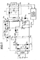
- FIG. 7 is an illustration of the resulting device, in which the primary inductor L 1 is connected via the reverse-blocking diode D 5 to the junction between transformer primary N 1 and switch Q 1 as in FIG. 5. This device gains the same advantages as do the FIGS. 5 and 6 embodiments.
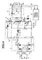
- the ancillary charging circuit 7 b is additionally modifiable as shown at 7 b in FIG. 8, which shows a further preferred embodiment of the invention that is similar in all the other respects to that of FIG. 6.
- the modified ancillary charging circuit 7 b has only the transformer ancillary winding N 3 and ancillary diode D 6 . Connected between the second rectifier output conductor 44 and smoothing capacitor C 1 via the ancillary diode D 6 , the transformer ancillary N 3 is assumed to possess leakage inductance.
- FIG. 8 embodiment offers the same advantages as does that of FIG. 6 except for the lack of smoothing effects by the reactor L 1 and capacitor C 2 of the FIG. 6 ancillary charging circuit 7 a . Counterbalancing this shortcoming are the simplicity in construction and compactness in size of the ancillary charging circuit 7 b .
- FIG. 8 ancillary charging circuit 7 b lends itself to use with the transformer 5 a of FIGS. 5 and 7. To this end, as indicated by the broken line in FIG. 8, the cathode of the reverse-blocking diode D 5 may be connected to the junction between transformer primary N 1 and switch Q 1 instead of to the tap 9.
- the switching power supply of FIG. 9 is similar to that of FIG. 6 except that a further modified transformer 5 b , a further modified ancillary charging circuit 7 c , and a modified rectifying and smoothing circuit 6 a are used in place of the transformer 5, ancillary charging circuit 7 a , and rectifying and smoothing circuit 6, respectively, of the FIG. 6 embodiment.
- the FIG. 9 transformer 5 b is similar to the FIG. 6 transformer 5 except that, as indicated by the dots in FIG. 9, the secondary winding N 2 and ancillary winding N 3 are both opposite in polarity to their FIG. 6 counterparts.
- the FIG. 9 ancillary charging circuit 7 c differs from the FIG. 6 ancillary charging circuit 7 a in the polarity of the transformer ancillary winding N 3 .
- the FIG. 9 rectifying and smoothing circuit 6 a differs from the FIG. 6 rectifying and smoothing circuit 6 in additionally comprising a choke or a smoothing inductor L 0 and a smoothing diode D a .
- the smoothing inductor L 0 is connected between rectifying diode D 0 and smoothing capacitor C 0 .
- the smoothing diode D a is connected n parallel with the serial connection of inductor L 0 and capacitor C 0 .
- a forward d.c.-to-d.c. converter is constituted of the smoothing capacitor C 1 , transformer 5 b , switch Q 1 , and rectifying and smoothing circuit 6 a .
- the diode D 0 will be forward biased by the voltage developing across the transformer secondary N 2 during the conducting periods of the switch Q 1 , with the consequent charging of the capacitor C 0 .
- the ancillary capacitor C 2 will also be charged by the voltage developing across the transformer ancillary N 3 during the conducting periods of the switch Q 1 .
- FIG. 9 device operates the same way as that of FIG. 6 except for how the ancillary capacitor C 2 and the output smoothing capacitor C 0 are charged, gaining the same advantages therewith.
- the FIG. 9 device is modifiable to include the transformer 5 a of FIGS. 5 and 7, by the cathode of the reverse-blocking diode D 5 may be connected to the junction between transformer primary N 1 and switch Q 1 , as indicated by the broken line in FIG. 9, instead of to the tap 9.
- An additional possible modification of the FIG. 9 embodiment is the omission of the capacitor C 2 , inductor L 2 and second diode D 7 from the ancillary charging circuit 7 c .
- the switching power supply is here shown comprising a modified rectifier circuit 4 a and modified ancillary charging circuit 7 d in places of the rectifier circuit 4 and ancillary charging circuit 7, respectively, of the FIG. 1 embodiment and is identical therewith in all the other respects.
- the modified rectifier circuit 4 a has two diodes D 11 and D 12 in addition to the four noted diodes D 1 - D 4 .
- the fifth diode D 11 has its anode connected to the first a.c. input conductor 41, and its cathode to the second rectifier output conductor 44.
- the sixth diode D 12 has its anode connected to the second a.c. input conductor 42, and its cathode to the second rectifier output conductor 44.
- the second rectifier output conductor 44 is therefore supplied not with the outputs from the first and third diodes D 1 and D 3 but with the outputs from fifth and sixth diodes D 11 and D 12 .
- These diodes D 11 and D 12 are substantially equal in electrical characteristics to the diodes D 1 and D 3 , so that the voltage between second rectifier output conductor 44 and ground-potential conductor 45 is substantially equal to the voltage V 4 between first rectifier output conductor 43 and ground-potential conductor 45.
- the modified ancillary charging circuit 7 d is similar to the FIG. 1 ancillary charging circuit 7 except for the absence of the diode D 7 .
- the modified circuit 7 d will nevertheless function just like the original circuit 7 as the two additional diodes D 11 and D 12 of the rectifier circuit 4 a serve to block reverse current flow.
- the diodes D 11 and D 12 are high-frequency diodes capable of responding to changes in the current through the ancillary inductor L 2 with the repeated conduction and non-conduction of the switch Q 1 .
- the omission of the diode D 7 is inadvisable in cases where low-frequency diodes are used at D 11 and D 12 .
Landscapes
- Engineering & Computer Science (AREA)
- Power Engineering (AREA)
- Rectifiers (AREA)
- Dc-Dc Converters (AREA)
Abstract
Description
Claims (12)
- A switching power supply capable of translating a.c. voltage into d.c. voltage, comprising a rectifier circuit (4 or 4 a ) connected to a pair of a.c. input terminals (1 and 2) for rectifying a.c. input voltage, the rectifier circuit having a first output conductor (43) and a second output conductor (44) for outputting a first and a second rectifier output voltage which are of approximately the same magnitude and a third output conductor (45), a transformer (5, 5 a or 5 b ) having a primary winding (N 1), a rectifying and smoothing circuit (6 or 6 a ) connected between the transformer and a pair of d.c. output terminals for providing the d.c. output voltage, an inductor (L 1) for improvement of the power factor of the input terminals, a smoothing capacitor (C 1) connected between the first output conductor and the third output conductor of the rectifier circuit via at least part of the primary winding (N 1) and the inductor (L 1), a switch (Q 1) connected between the first output conductor (43) and the third output conductor (45) of the rectifier circuit via at least the inductor (L 1), and in parallel with the smoothing capacitor (C 1) via the primary winding (N 1), a switch control circuit (8) connected to the switch for on-off control of the switch (Q 1) at a repetition frequency higher than the frequency of the a.c. input voltage, characterized in that an ancillary charging circuit (7, 7 a , 7 b , 7 c or 7 d ) is provided which comprises an ancillary winding (N 3) electromagnetically coupled to a primary winding (N 1) of the transformer (5, 5 a or 5 b ), the ancillary winding being connected between the second output conductor (44) of the rectifier circuit (4 or 4a) and the smoothing capacitor (C 1).
- A switching power supply as claimed in claim 1, characterized in that the ancillary charging circuit (7) further comprises an ancillary capacitor (C 2) connected to one extremity of the ancillary winding (N 3), another extremity of which is connected to the primary winding (N 1) of the transformer (5) and to the smoothing capacitor (C 1), an ancillary diode (D 6) connected in parallel with the ancillary winding (N 3) via the ancillary capacitor (C 2), and an ancillary inductor (L 2) connected between the second output conductor (44) of the rectifier circuit (4 or 4 a ) and a junction between the ancillary capacitor (C 2) and the ancillary diode (D 6).
- A switching power supply as claimed in claim 2, characterized in that the ancillary charging circuit (7) further comprises a second ancillary diode (D 7) connected in series with the ancillary inductor (L 2).
- A switching power supply as claimed in claim 1, characterized in that the ancillary charging circuit (7 a ) further comprises an ancillary diode (D 6) connected to one extremity of the ancillary winding (N 3), another extremity of which is connected to the primary winding (N 1) of the transformer (5) and to the smoothing capacitor (C 1), an ancillary capacitor (C 2) connected in parallel with the ancillary winding via the ancillary diode (D 6), and an ancillary inductor (L 2) connected between the second output conductor (44) of the rectifier circuit (4 or 4 a ) and a junction between the ancillary diode (D 6) and the ancillary capacitor (C 2).
- A switching power supply as claimed in claim 4, characterized in that the ancillary charging circuit (7 a ) further comprises a second ancillary diode (D 7) connected in series with the ancillary inductor (L 2).
- A switching power supply as claimed in claim 1, characterized in that a reverse-blocking diode (D 5) is connected in series with the induc-tor (L 1).
- A switching power supply as claimed in claim 1, wherein the primary winding (N 1) of the transformer (5) is tapped (at 9) to provide two divisions (N 1 a and N 1 b ) thereof, characterized in that the inductor (L 1) and one division (N 1 b ) of the transformer primary winding and the switch (Q 1) form a serial circuit, which serial circuit is connected between the first output conductor (43) and the third output conductor (45) of the rectifier circuit (4 or 4 a ), and that the smoothing capacitor (C 1) is connected in parallel with a serial circuit of both divisions (N 1 a and N 1 b ) of the transformer primary winding and the switch (Q 1).
- A switching power supply as claimed in claim 1, characterized in that the complete transformer primary winding (N 1) forms a serial circuit with the inductor (L 1) and the smoothing capacitor (C 1), which serial circuit is connected between the first output conductor (43) and the third output conductor (45) of the rectifier circuit (4 or 4 a ), and that a serial circuit of the complete transformerprimary winding (N 1) and the switch (Q 1) is connected in parallel with the smoothing capacitor (C 1).
- A switching power supply as claimed in claim 1, wherein the transformer (5 or 5 a ) has a secondary winding (N 2) electromagnetically coupled to the primary winding (N 1), characterized in that the rectifying and smoothing circuit (6) comprises a rectifying device (D 0) connected to the secondary winding (N 2) of the transformer and adapted to be made conductive by a voltage developing across the transformer secondary winding during the nonconductive periods of the switch (Q 1), and an additional capacitor (C 0) connected in parallel with the transformer secondary winding via the rectifying device.
- A switching power supply as claimed in claim 1, wherein the transformer (5 b ) has a secondary winding (N 2) electromagnetically coupled to the primary winding (N 1), characterized in that the rectifying and smoothing circuit (6 a ) comprises a rectifying device (D 0) connected to the secondary winding (N 2) of the transformer and adapted to be made conductive by a voltage developing across the transformer secondary winding during the conductive periods of the switch (Q 1), and an additional capacitor (C 0) connected in parallel with the transformer secondary winding via the rectifying device.
- A switching power supply as claimed in claim 1, characterized in that the rectifier circuit (4) comprises a first diode (D 1) having a first electrode connected to a first input conductor (41) of the rectifier circuit, a second diode (D 2) having a first electrode connected to the third output conductor (45) of the rectifier circuit and a second electrode connected to the first input conductor (41) of the rectifier circuit, a third diode (D 3) having a first electrode connected to a second input conductor (42) of the rectifier circuit and a second electrode connected to a second electrode of the first diode (D 1), with a junction (48) between the second electrodes of the first and the third diode (D 1 and D 3) being connected to the first and the second output conductor (43 and 44) of the rectifier circuit, and a fourth diode (D4) having a first electrode connected to the third output conductor (45) of the rectifier circuit, and a second electrode connected to the second input conductor (42) of the rectifier circuit.
- A switching power supply as claimed in claim 1, characterized in that the rectifier circuit (4 a ) comprises a first diode (D 1) having a first electrode connected to a first input conductor (41) of the rectifier circuit (4 a ) and a second electrode connected to the first output conductor (43) of the rectifier circuit, a second diode (D 2) having a first electrode connected to the third output conductor (45) of the rectifier circuit and a second electrode connected to the first input conductor (41) of the rectifier circuit, a third diode (D 3) having a first electrode connected to a second input conductor (42) of the rectifier circuit and a second electrode connected to the first output conductor (43) of the rectifier circuit, a fourth diode (D 4) having a first electrode connected to the third output conductor (45) of the rectifier circuit and a second electrode connected to the second input conductor (42) of the rectifier circuit, a fifth diode (D 11) having a first electrode connected to the first input conductor (41) of the rectifier circuit and a second electrode connected to the second output conductor (44) of the rectifier circuit, and a sixth diode (D 12) having a first electrode connected to the second input conductor (42) of the rectifier circuit and a second electrode connected to the second output conductor (44) of the rectifier circuit.
Applications Claiming Priority (2)
| Application Number | Priority Date | Filing Date | Title |
|---|---|---|---|
| JP2001119916 | 2001-04-18 | ||
| JP2001119916A JP3496717B2 (en) | 2001-04-18 | 2001-04-18 | Switching power supply |
Publications (3)
| Publication Number | Publication Date |
|---|---|
| EP1251630A2 true EP1251630A2 (en) | 2002-10-23 |
| EP1251630A3 EP1251630A3 (en) | 2003-05-02 |
| EP1251630B1 EP1251630B1 (en) | 2005-07-20 |
Family
ID=18970046
Family Applications (1)
| Application Number | Title | Priority Date | Filing Date |
|---|---|---|---|
| EP02007945A Expired - Lifetime EP1251630B1 (en) | 2001-04-18 | 2002-04-09 | Switching power supply |
Country Status (4)
| Country | Link |
|---|---|
| US (1) | US6466463B1 (en) |
| EP (1) | EP1251630B1 (en) |
| JP (1) | JP3496717B2 (en) |
| DE (1) | DE60205058T2 (en) |
Cited By (1)
| Publication number | Priority date | Publication date | Assignee | Title |
|---|---|---|---|---|
| RU2480888C2 (en) * | 2007-11-26 | 2013-04-27 | Конинклейке Филипс Электроникс Н.В. | Circuit of power ratio control and grid source of power supply |
Families Citing this family (13)
| Publication number | Priority date | Publication date | Assignee | Title |
|---|---|---|---|---|
| WO2001057998A1 (en) * | 2000-02-02 | 2001-08-09 | The Regents Of The University Of California | A single-stage power factor correction method to reduce energy storage capacitor voltage and circuit for same |
| JP3374917B2 (en) * | 2001-02-16 | 2003-02-10 | サンケン電気株式会社 | Switching power supply |
| JP3475943B2 (en) * | 2001-06-29 | 2003-12-10 | サンケン電気株式会社 | Switching power supply |
| JP4126526B2 (en) * | 2001-09-28 | 2008-07-30 | サンケン電気株式会社 | Switching power supply |
| JP3659240B2 (en) * | 2001-11-16 | 2005-06-15 | ソニー株式会社 | Switching power supply circuit |
| DE10257578A1 (en) * | 2001-12-21 | 2003-07-03 | Fuji Electric Co Ltd | Switching Power Supply |
| US6844779B2 (en) * | 2003-06-19 | 2005-01-18 | The United States Of America As Represented By The Secretary Of The Air Force | Optically isolated bias control circuit |
| JP2005261112A (en) * | 2004-03-12 | 2005-09-22 | Sanken Electric Co Ltd | Dc-dc converter |
| US7356309B2 (en) * | 2004-03-26 | 2008-04-08 | Broadcom Corporation | Directional coupler for communication system |
| KR102034149B1 (en) * | 2013-01-10 | 2019-10-18 | 엘지이노텍 주식회사 | Single Stage AC/DC converter |
| CN106602537B (en) * | 2017-02-28 | 2019-12-03 | 深圳市华星光电技术有限公司 | A kind of voltage absorpting circuit |
| JP7676212B2 (en) * | 2021-04-30 | 2025-05-14 | キヤノン株式会社 | Power supply device and image forming apparatus |
| JP7767113B2 (en) * | 2021-11-02 | 2025-11-11 | キヤノン株式会社 | Power supply device and image forming apparatus |
Family Cites Families (5)
| Publication number | Priority date | Publication date | Assignee | Title |
|---|---|---|---|---|
| EP0964504B1 (en) * | 1994-01-28 | 2004-05-06 | Matsushita Electric Industrial Co., Ltd. | Switching power source apparatus |
| JP3127979B2 (en) | 1994-11-28 | 2001-01-29 | サンケン電気株式会社 | DC power supply |
| KR970031200A (en) * | 1995-11-13 | 1997-06-26 | 이준 | Single Power Stage High Power Factor Converter |
| JP2900876B2 (en) * | 1996-03-19 | 1999-06-02 | サンケン電気株式会社 | Display power supply |
| JP2991181B2 (en) * | 1998-02-27 | 1999-12-20 | 富士電機株式会社 | Switching power supply |
-
2001
- 2001-04-18 JP JP2001119916A patent/JP3496717B2/en not_active Expired - Fee Related
-
2002
- 2002-04-09 US US10/118,713 patent/US6466463B1/en not_active Expired - Fee Related
- 2002-04-09 EP EP02007945A patent/EP1251630B1/en not_active Expired - Lifetime
- 2002-04-09 DE DE60205058T patent/DE60205058T2/en not_active Expired - Fee Related
Cited By (1)
| Publication number | Priority date | Publication date | Assignee | Title |
|---|---|---|---|---|
| RU2480888C2 (en) * | 2007-11-26 | 2013-04-27 | Конинклейке Филипс Электроникс Н.В. | Circuit of power ratio control and grid source of power supply |
Also Published As
| Publication number | Publication date |
|---|---|
| JP3496717B2 (en) | 2004-02-16 |
| EP1251630B1 (en) | 2005-07-20 |
| EP1251630A3 (en) | 2003-05-02 |
| DE60205058T2 (en) | 2006-05-24 |
| JP2002320388A (en) | 2002-10-31 |
| US20020154522A1 (en) | 2002-10-24 |
| DE60205058D1 (en) | 2005-08-25 |
| US6466463B1 (en) | 2002-10-15 |
Similar Documents
| Publication | Publication Date | Title |
|---|---|---|
| US6574122B2 (en) | Low-noise switching power supply | |
| US6639813B2 (en) | Zero-voltage-switching power supply | |
| US5303138A (en) | Low loss synchronous rectifier for application to clamped-mode power converters | |
| EP0851566B1 (en) | Half-bridge zero-voltage-switched PWM flyback DC/DC converter | |
| EP1251630B1 (en) | Switching power supply | |
| TW588497B (en) | Synchronous rectifier of intermittent control and its control method | |
| JPS62166772A (en) | Forward converter used for changing electric source | |
| EP1289110B1 (en) | Switching power supply | |
| US6671188B2 (en) | Soft-switching power supply | |
| US7023711B2 (en) | Power supply circuit and electronic apparatus | |
| US11973440B2 (en) | Isolated DC/DC converter with secondary-side full bridge diode rectifier and asymmetrical auxiliary capacitor | |
| JP4198379B2 (en) | Power supply device having a DC / DC converter | |
| CN113302828B (en) | Voltage conversion circuits and electronic devices | |
| EP0964504B1 (en) | Switching power source apparatus | |
| US7157887B2 (en) | Direct amplitude modulation for switch mode power supplies | |
| JP3034860B1 (en) | Power regeneration device | |
| EP1172922B1 (en) | Universal switched power converter | |
| US6081435A (en) | Cross-conduction limiting circuit, method of operation thereof and DC/DC converter employing the same | |
| RU2186452C2 (en) | Half-bridge dc voltage converter | |
| SU1390740A1 (en) | Single-cycle d.c.-to-d.c. voltage converter | |
| JPH04251559A (en) | Dc power supply | |
| SU1742956A1 (en) | Two-channel dc/dc converter | |
| JPH07312868A (en) | Switching power converter | |
| JPH0340754A (en) | Power source device | |
| JPH104684A (en) | Switching power unit |
Legal Events
| Date | Code | Title | Description |
|---|---|---|---|
| PUAI | Public reference made under article 153(3) epc to a published international application that has entered the european phase |
Free format text: ORIGINAL CODE: 0009012 |
|
| AK | Designated contracting states |
Kind code of ref document: A2 Designated state(s): AT BE CH CY DE DK ES FI FR GB GR IE IT LI LU MC NL PT SE TR |
|
| AX | Request for extension of the european patent |
Free format text: AL;LT;LV;MK;RO;SI |
|
| PUAL | Search report despatched |
Free format text: ORIGINAL CODE: 0009013 |
|
| AK | Designated contracting states |
Designated state(s): AT BE CH CY DE DK ES FI FR GB GR IE IT LI LU MC NL PT SE TR |
|
| AX | Request for extension of the european patent |
Extension state: AL LT LV MK RO SI |
|
| 17P | Request for examination filed |
Effective date: 20030821 |
|
| AKX | Designation fees paid |
Designated state(s): DE FR GB |
|
| 17Q | First examination report despatched |
Effective date: 20040127 |
|
| GRAP | Despatch of communication of intention to grant a patent |
Free format text: ORIGINAL CODE: EPIDOSNIGR1 |
|
| GRAS | Grant fee paid |
Free format text: ORIGINAL CODE: EPIDOSNIGR3 |
|
| GRAA | (expected) grant |
Free format text: ORIGINAL CODE: 0009210 |
|
| AK | Designated contracting states |
Kind code of ref document: B1 Designated state(s): DE FR GB |
|
| REG | Reference to a national code |
Ref country code: GB Ref legal event code: FG4D |
|
| REF | Corresponds to: |
Ref document number: 60205058 Country of ref document: DE Date of ref document: 20050825 Kind code of ref document: P |
|
| PG25 | Lapsed in a contracting state [announced via postgrant information from national office to epo] |
Ref country code: GB Free format text: LAPSE BECAUSE OF NON-PAYMENT OF DUE FEES Effective date: 20060409 |
|
| PLBE | No opposition filed within time limit |
Free format text: ORIGINAL CODE: 0009261 |
|
| STAA | Information on the status of an ep patent application or granted ep patent |
Free format text: STATUS: NO OPPOSITION FILED WITHIN TIME LIMIT |
|
| 26N | No opposition filed |
Effective date: 20060421 |
|
| EN | Fr: translation not filed | ||
| PG25 | Lapsed in a contracting state [announced via postgrant information from national office to epo] |
Ref country code: FR Free format text: LAPSE BECAUSE OF FAILURE TO SUBMIT A TRANSLATION OF THE DESCRIPTION OR TO PAY THE FEE WITHIN THE PRESCRIBED TIME-LIMIT Effective date: 20060915 |
|
| GBPC | Gb: european patent ceased through non-payment of renewal fee |
Effective date: 20060409 |
|
| PGFP | Annual fee paid to national office [announced via postgrant information from national office to epo] |
Ref country code: DE Payment date: 20080429 Year of fee payment: 7 |
|
| PG25 | Lapsed in a contracting state [announced via postgrant information from national office to epo] |
Ref country code: FR Free format text: LAPSE BECAUSE OF FAILURE TO SUBMIT A TRANSLATION OF THE DESCRIPTION OR TO PAY THE FEE WITHIN THE PRESCRIBED TIME-LIMIT Effective date: 20050720 |
|
| PG25 | Lapsed in a contracting state [announced via postgrant information from national office to epo] |
Ref country code: DE Free format text: LAPSE BECAUSE OF NON-PAYMENT OF DUE FEES Effective date: 20091103 |