EP1249971A2 - Network Interface Using Programmable Delay and Frequency Doubler - Google Patents
Network Interface Using Programmable Delay and Frequency Doubler Download PDFInfo
- Publication number
- EP1249971A2 EP1249971A2 EP02100269A EP02100269A EP1249971A2 EP 1249971 A2 EP1249971 A2 EP 1249971A2 EP 02100269 A EP02100269 A EP 02100269A EP 02100269 A EP02100269 A EP 02100269A EP 1249971 A2 EP1249971 A2 EP 1249971A2
- Authority
- EP
- European Patent Office
- Prior art keywords
- data
- clock signal
- input
- network device
- external clock
- Prior art date
- Legal status (The legal status is an assumption and is not a legal conclusion. Google has not performed a legal analysis and makes no representation as to the accuracy of the status listed.)
- Granted
Links
Images






Classifications
-
- H—ELECTRICITY
- H03—ELECTRONIC CIRCUITRY
- H03L—AUTOMATIC CONTROL, STARTING, SYNCHRONISATION OR STABILISATION OF GENERATORS OF ELECTRONIC OSCILLATIONS OR PULSES
- H03L7/00—Automatic control of frequency or phase; Synchronisation
-
- H—ELECTRICITY
- H04—ELECTRIC COMMUNICATION TECHNIQUE
- H04J—MULTIPLEX COMMUNICATION
- H04J3/00—Time-division multiplex systems
- H04J3/02—Details
- H04J3/06—Synchronising arrangements
- H04J3/0635—Clock or time synchronisation in a network
- H04J3/0685—Clock or time synchronisation in a node; Intranode synchronisation
- H04J3/0697—Synchronisation in a packet node
-
- H—ELECTRICITY
- H04—ELECTRIC COMMUNICATION TECHNIQUE
- H04L—TRANSMISSION OF DIGITAL INFORMATION, e.g. TELEGRAPHIC COMMUNICATION
- H04L25/00—Baseband systems
- H04L25/02—Details ; arrangements for supplying electrical power along data transmission lines
- H04L25/14—Channel dividing arrangements, i.e. in which a single bit stream is divided between several baseband channels and reassembled at the receiver
-
- H—ELECTRICITY
- H04—ELECTRIC COMMUNICATION TECHNIQUE
- H04L—TRANSMISSION OF DIGITAL INFORMATION, e.g. TELEGRAPHIC COMMUNICATION
- H04L7/00—Arrangements for synchronising receiver with transmitter
- H04L7/0008—Synchronisation information channels, e.g. clock distribution lines
-
- H—ELECTRICITY
- H04—ELECTRIC COMMUNICATION TECHNIQUE
- H04L—TRANSMISSION OF DIGITAL INFORMATION, e.g. TELEGRAPHIC COMMUNICATION
- H04L7/00—Arrangements for synchronising receiver with transmitter
- H04L7/02—Speed or phase control by the received code signals, the signals containing no special synchronisation information
- H04L7/033—Speed or phase control by the received code signals, the signals containing no special synchronisation information using the transitions of the received signal to control the phase of the synchronising-signal-generating means, e.g. using a phase-locked loop
- H04L7/0337—Selecting between two or more discretely delayed clocks or selecting between two or more discretely delayed received code signals
- H04L7/0338—Selecting between two or more discretely delayed clocks or selecting between two or more discretely delayed received code signals the correction of the phase error being performed by a feed forward loop
-
- H—ELECTRICITY
- H04—ELECTRIC COMMUNICATION TECHNIQUE
- H04L—TRANSMISSION OF DIGITAL INFORMATION, e.g. TELEGRAPHIC COMMUNICATION
- H04L7/00—Arrangements for synchronising receiver with transmitter
- H04L7/0016—Arrangements for synchronising receiver with transmitter correction of synchronization errors
- H04L7/0033—Correction by delay
-
- H—ELECTRICITY
- H04—ELECTRIC COMMUNICATION TECHNIQUE
- H04L—TRANSMISSION OF DIGITAL INFORMATION, e.g. TELEGRAPHIC COMMUNICATION
- H04L7/00—Arrangements for synchronising receiver with transmitter
- H04L7/0091—Transmitter details
-
- H—ELECTRICITY
- H04—ELECTRIC COMMUNICATION TECHNIQUE
- H04L—TRANSMISSION OF DIGITAL INFORMATION, e.g. TELEGRAPHIC COMMUNICATION
- H04L7/00—Arrangements for synchronising receiver with transmitter
- H04L7/02—Speed or phase control by the received code signals, the signals containing no special synchronisation information
- H04L7/033—Speed or phase control by the received code signals, the signals containing no special synchronisation information using the transitions of the received signal to control the phase of the synchronising-signal-generating means, e.g. using a phase-locked loop
- H04L7/0337—Selecting between two or more discretely delayed clocks or selecting between two or more discretely delayed received code signals
Definitions
- the invention relates to systems and methods for transmitting data between network devices.
- the invention relates to systems and methods for linking network devices at high speeds using double the data rate (DDR).
- DDR double the data rate
- Ethernet technology which is based upon numerous IEEE Ethernet standards, is one example of computer networking technology which has been able to be modified and improved to remain a viable computing technology.
- SWITCHED AND FAST ETHERNET is one example of computer networking technology which has been able to be modified and improved to remain a viable computing technology.
- SWITCHED AND FAST ETHERNET is one example of computer networking technology which has been able to be modified and improved to remain a viable computing technology.
- SWITCHED AND FAST ETHERNET by Breyer and Riley (Ziff Davis, 1996)
- IEEE publications relating to IEEE 802 standards can be found, for example, in SWITCHED AND FAST ETHERNET, by Breyer and Riley (Ziff Davis, 1996), and numerous IEEE publications relating to IEEE 802 standards.
- OSI Open Systems Interconnect
- Thickwire, thinwire, twisted pair, and optical fiber are examples of media which has been used for computer networks.
- Switches as they relate to computer networking and to ethernet, are hardware based devices which control the flow of data packets or cells based upon destination address information which is available in each packet.
- a properly designed and implemented switch should be capable of receiving a packet and switching the packet to an appropriate output port at what is referred to wirespeed or linespeed, which is the maximum speed capability of the particular network.
- Current basic Ethernet wirespeeds typically range from 10 Megabits per second (Mps) up to 10,000 Mps, or 10 Gigabits per second.
- Mps Megabits per second
- 10 Gigabits per second As speed has increased, design constraints and design requirements have become more and more complex with respect to following appropriate design and protocol rules and providing a low cost, commercially viable solution.
- One system or method of improving linking performance includes increasing the speed of the external clock or of the board clock speed.
- Faster clock speed means faster data speeds.
- faster and more reliable clocks are more expensive and are therefore not preferred by manufacturers.
- devices are often constructed on printed circuit boards (PCB), which are manufactured to within certain tolerances.
- PCB printed circuit boards
- On board clock speeds for PCBs are often limited by manufacturing tolerances, and mass produced PCB s may not be able to handle the same clock cycle rates as silicon chips.
- Increasing the quality of a PCB to handle faster clock speeds decreases manufacturing yield, and can also be very expensive. Therefore, new and improved systems and methods are needed for increasing linking speeds between network devices without increasing the speed external clocks or changing the design of the PCB.
- Such systems and methods should also take into account variations in chip material speeds due to process or operating conditions.
- a network device which includes an input, at least one port, a frequency doubler, a data I/O device, and a variable delay circuit.
- the input is for receiving an external clock signal.
- the frequency doubler is coupled to the input and configured to receive an input signal and output an output signal with a frequency double that of the input signal.
- the data I/O device is configured to output data to the at least one port based on a reference clock signal.
- the variable delay circuit is located between the data I/O device and at least one port.
- An external clock signal received at the input is input into the frequency doubler.
- the output signal of the frequency doubler is applied to the data I/O device as the reference clock signal, and the output data is delayed by the variable delay circuit.
- a network device which includes an input means, at least one port, a frequency doubler means, a data I/O means, and a variable delay circuit means.
- the input means is for receiving an external clock signal.
- the frequency doubler means is coupled to the input for receiving an input signal and outputting an output signal having a frequency double that of the input signal.
- the data I/O means is for outputting data to the at least one port based on a reference clock signal.
- An external clock signal received at the input means is input into the frequency doubler means.
- the output signal of the frequency doubler means is applied to the data I/O device as the reference clock signal.
- the output data is delayed by the variable delay circuit means.
- a method for linking network devices including a step of receiving an external clock signal at a first device.
- the external clock signal received by the first device is split into a first input clock signal and a second input clock signal within the first device.
- the frequency of the first input clock signal is doubled.
- the doubled clock signal is applied to data to be outputted of the first device at double the data rate of the external clock signal, the data being outputted at a port of the first device.
- the data to be outputted is delayed.
- the second input clock signal is provided to the port of the first device.
- the data is variably delayed to synchronize the data with the second input clock signal, and the data and the second input clock signal are transmitted out of the first device at the port.
- a network device which includes a first switch and a second switch.
- the first switch includes an input, a first plurality of ports, a frequency doubler coupled to the input and configured to receive an input signal and output an output signal with a frequency double that of the input signal, an I/O device configured to output data to at least one of the plurality of ports based on a first reference clock signal, and a variable delay circuit.
- the second switch includes a second plurality of ports and a double data rate receiving unit configured to receive data and a second reference clock signal from at least one of the second plurality of ports, and to extract data based on a rising edge and a falling edge of the second reference clock signal.
- the device also includes an external clock couple to the first switch.
- a circuit is provided coupling a first link port of the first plurality of ports to a second link port of the second plurality of ports.
- An external clock signal received as the input of the first switch from the external clock is input into the frequency doubler.
- the output of the frequency doubler is input to the I/O device as a first reference clock signal.
- the I/O device outputs the data to the first link port via the variable delay circuit.
- the variable delay circuit delays the data.
- the switch is configured to output the data and the external clock signal from the link port to the second link port of the second switch via the circuit.
- the second switch is configured to receive the data and the external clock signal and input the external clock signal as a second reference clock and the data to the double data rate receiving unit.
- the double data rate receives unit the data.
- a network device which includes a first switch means, a second switch means, an external clock means, and a circuit means
- the first switch means includes an input mean, a first plurality of ports, a frequency doubler means coupled to the input for receiving an input signal and outputting an output signal with a frequency double that of the input signal, an I/O device means for outputting data to at least one of the plurality of ports based on a first reference clock signal, and a variable delay circuit means.
- the second switch means includes a second plurality of ports and a double data rate receiving means for receiving data and a second reference clock signal from at least one of the second plurality of ports, and for extracting data based on a rising edge and a falling edge of the second reference clock signal.
- the external clock means is for generating an external clock signal coupled to the first switch.
- the circuit means is for coupling a first link port of the first plurality of ports to a second link port of the second plurality of ports.
- the first switch means is configured to receive an external clock signal via the input means from the external clock means and input the external clock signal into the frequency doubler means, to input the output of the frequency doubler means to the I/O device means as a first reference clock signal, to output the data from the I/O device means to the first link port via the variable delay circuit means, the data being delayed by the variable delay circuit means, and to output the data and the external clock signal from the link port to the second link port via the circuit means.
- the second switch is configured to receive the data and the external clock signal and input the external clock signal as a second reference clock, and the data to the double data rate receiving means.
- the double data rate receiving unit is configured to extract the data at double data rate.
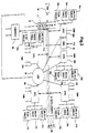
- Figure 1 is a general block diagram of an exemplary network device according to the invention.
- FIG. 2 is a detailed block diagram of a network switch according to the invention.
- Figure 3 illustrates an exemplary configuration of linked network devices according to an embodiment of the present invention
- Figure 4 illustrates another exemplary configuration of linked network devices according to an embodiment of the present invention
- Figure 5 illustrates another exemplary configuration of linked network devices according to an embodiment of the present invention
- Figure 6 illustrates another exemplary configuration of linked network devices according to an embodiment of the present invention
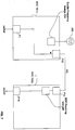
- Figure 7 is a block diagram of linked network devices according to an embodiment of the present invention.
- Figure 8 is a schematic diagram of a link configuration according to an embodiment of the present invention.
- Figure 9 is a flow chart of a method for linking network devices according to an embodiment of the present invention.
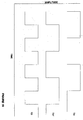
- Figure 10 is a graph of input clock signals and a doubled clock signal according to the present invention.
- FIG. 1 is a basic block diagram of an exemplary high speed network device to which the present invention is applicable.
- An exemplary configuration of a network switch is shown.
- a switch on chip (SOC) 10 is functionally connected to external devices 11, external memory 12, fast ethernet ports 13, and gigabit ethernet ports 15.
- fast ethernet ports 13 will be considered low speed ethernet ports, since they are capable of operating at speeds ranging from 10 Mbps to 100 Mbps in this example, while the gigabit ethernet ports 15 or link ports, which are high speed ethernet ports, are capable of operating at 2500 Mbps or higher in this example.
- External devices 11 could include other switching devices for expanding switching capabilities, or other devices as may be required by a particular application.
- External memory 12 can be additional off chip memory, which is in addition to internal memory (on chip) which is located on SOC 10, which will be discussed below.
- CPU 52 can be used as desired to program SOC 10 with rules which are appropriate to control packet processing. However, once SOC 10 is appropriately programmed or configured, SOC 10 operates, as much as possible, in a free running manner without communicating with CPU 52.
- CPU 52 does not control every aspect of the operation of SOC 10, because CPU 52 performance requirements in this example, at least with respect to SOC 10, are fairly low. A less powerful and therefore less expensive CPU 52 can therefore be used when compared to known network switches.
- SOC 10 utilizes external memory 12 in an efficient manner so that the cost and performance requirements of memory 12 can be reduced. Internal memory on SOC 10, as will be discussed below, is also configured to maximize switching throughput and minimize costs.
- port speeds described are merely exemplary and ports may be configured to handle a variety of speeds faster and slower than the speeds discussed herein.
- FIG. 2 illustrates a more detailed block diagram of the functional elements of SOC 10.
- SOC 10 includes a plurality of modular systems on chip, with each modular system, although being on the same chip, being functionally separate from other modular systems. Therefore, each module can efficiently operate in parallel with other modules, and this configuration enables a significant amount of freedom in updating and re engineering SOC 10.
- switch configurations or network device configurations may be utilized to produce the present invention.
- SOC 10 may include a plurality of Ethernet Port Interface Controllers (EPIC) 20a, 20b, 20c, etc., a plurality of Gigabit Port Interface Controllers (GPIC) 30a, 30b, etc., a CPU Management Interface Controller (CMIC) 40, a Common Buffer Memory Pool (CBP) 50, a Pipelined Memory Management Unit (PMMU) 70, including a Common Buffer Manager (CBM) 71, and a system wide bus structure referred to as CPS channel 80.
- the PMMU 70 includes memory management means and communicates with external memory 12, which includes a Global Buffer Memory Pool (GBP) 60.
- the CPS channel 80 comprises C channel 81, P channel 82, and S channel 83.
- the CPS channel is also referred to as the cell protocol sideband channel, and is a 17 Gbps channel which glues or interconnects the various modules together.
- other high speed interconnects can be provided, as shown as an extendible high speed interconnect.
- this interconnect can be in the form of an interconnect port interface controller (IPIC) 90, which is capable of interfacing CPS channel 80 to external devices 11 through an extendible high speed interconnect link.
- IPIC interconnect port interface controller
- each EPIC 20a, 20b, and 20c generally referred to as EPIC 20, and GPIC 30a and 30b, generally referred to as GPIC 30, are closely interrelated with appropriate address resolution logic and layer three switching tables 21 a, 21 b, 21 c, 31 a, 31 b, rules tables 22a, 22b, 22c, 31a, 31b, and VLAN tables 23a, 23b, 23c, 31a, 31b.
- These tables will be generally referred to as 21, 31, 22, 32, 23, 33, respectively.
- EPIC 20 may support a number of fast ethernet ports 13 (8 are shown as an example), and switches packets to and/or from these ports as may be appropriate.
- the ports therefore, are connected to the network medium (coaxial, twisted pair, fiber, etc.) using known media connection technology, and communicates with the CPS channel 80 on the other side thereof.
- the interface of each EPIC 20 to the network medium can be provided through a Reduced Media Internal Interface (RMII), which enables the direct medium connection to SOC 10.
- RMII Reduced Media Internal Interface
- auto negotiation is an aspect of network communications, wherein the network is capable of negotiating a highest communication speed between a source and a destination based on the capabilities of the respective devices.
- the communication speed can vary, as noted previously, for example, between 10 Mbps and 100 Mbps, as an example.
- Auto negotiation capability therefore, is built directly into each EPIC 20 or GPIC 30 module.
- the address resolution logic (ARL) and layer three tables (ARL/L3) 21a, 21b, 21c, rules table 22a, 22b, 22c, and VLAN tables 23a, 23b, and 23c are configured to be part of, or interface with the associated EPIC in an efficient and expedient manner, in order to support wirespeed packet flow.
- the on chip memory which is searched in accordance with the present invention may comprise these tables, as is described below in more detail.
- Each EPIC 20 and GPIC 30 has separate ingress and egress functions. On the ingress side, self initiated and CPU initiated learning of level 2 address information can occur. Address resolution logic (ARL) is utilized to assist in this task. Address aging is built in as a feature, in order to eliminate the storage of address information which is no longer valid or useful.
- the EPIC and GPIC can also carry out layer 2 mirroring.
- a fast filtering processor (FFP) 141 may be incorporated into the EPIC, in order to accelerate packet forwarding and enhance packet flow.
- the EPIC and GPIC may include data transmitters and data receivers for transmitting and receiving data in accordance with the present invention.
- each port on each module of SOC 10 can have a separate ingress submodule 14 associated therewith. From an implementation perspective, however, in order to minimize the amount of hardware implemented on the single chip SOC 10, common hardware elements in the silicon can be used to implement a plurality of ingress submodules on each particular module.
- the configuration of SOC 10 discussed herein enables concurrent lookups and filtering. Layer two lookups, Layer three lookups and filtering occur simultaneously to achieve a high level of performance, which are described in better detail below.
- the EPIC and GPIC are capable of supporting packet polling based either as an egress management or class of service (COS) function. Rerouting/scheduling of packets to be transmitted can occur, as well as head of line (HOL) blocking notification, discussed later herein, packet aging, cell reassembly, and other functions associated with ethernet port interface.
- COS class of service
- Each GPIC 30 is similar to each EPIC 20, but in this embodiment, supports only one 2.5 gigabit ethernet port, and utilizes a port specific ARL table, rather than utilizing an ARL table which is shared with any other ports. Additionally, instead of an RMII, each GPIC port interfaces to the network medium utilizing a gigabit media independent interface (GMII).
- GMII gigabit media independent interface
- a CMIC 40 can act as a gateway between the SOC 10 and the host CPU.
- the communication can be, for example, along a PCI bus, or other acceptable communications bus.
- CMIC 40 can provide sequential direct mapped accesses between the host CPU 52 and the SOC 10.
- CPU 52, through the CMIC 40 will be able to access numerous resources on SOC 10, including MIB counters, programmable registers, status and control registers, configuration registers, ARL tables, port based VLAN tables, IEEE 802.1q VLAN tables, layer three tables, rules tables, CBP address and data memory, as well as GBP address and data memory.
- the CMIC 40 can include DMA support, DMA chaining and scatter gather, as well as master and target PCI64.
- the configuration of the SOC 10 can support fast Ethernet ports, gigabit ports, and extendible interconnect links as discussed above.
- the SOC configuration can also be "stacked" or linked , thereby enabling significant port expansion capability.
- a significant amount of concurrent lookups and filtering occurs as the packet comes in to ingress submodule 14 of an EPIC 20 or GPIC 30, with respect to layer two and layer three lookups, and fast filtering.
- FIG 3 illustrates an exemplary configuration where a plurality of SOCs 10(1)....10(n) are connected by link ports (not shown).
- SOCs 10(1) 10(n) include the elements which are illustrated in Figure 2.
- Figure 3 schematically illustrates CVP 50, MMU 70, EPICs 20 and GPICs 30 of each SOC 10.
- Interstack connection I is used to provide a stacking configuration between the switches, and can utilize, as an example, at least one gigabit uplink or other ports of each switch to provide a simplex or duplex stacking configuration as will be discussed below.
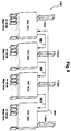
- Figure 4 illustrates a configuration wherein a plurality of SOCs 10(1) 10(4) are connected in a configuration using GPIC modules 30 to create a stack.
- each SOC 10 contains 24 low speed Ethernet ports having a maximum speed of 100 Megabits per second, and two 2.5 gigabit ports.
- the configuration of Figure 4 therefore, could result in 96 Ethernet ports and 4 usable 2.5 gigabit ports, with four other 2.5 gigabit ports being used to link the stack as what is called a stacked link.
- Interconnection as shown in Figure 4 results in what is referred to as a simplex ring, enabling unidirectional communication at a rate of 1 2.5 gigabits per second.
- All of the ports of the stack may be on the same VLAN, or a plurality of VLANs may be present on the stack. Multiple VLANs can be present on the same switch.
- the VLAN configurations are determined by the user, depending upon network requirements. This is true for all SOC 10 switch configurations. It should be noted, however, that these particular configurations used as examples only, and are not intended to limit the scope of the claimed invention.
- Figure 5 illustrates a second configuration of four stacked SOC 10 switches, SOC 10(1)...10(4). However, any number of switches could be stacked in this manner.
- the configuration of Figure 5 utilizes bi directional interstack links to create a full duplex configuration.
- the utilization of bi directional interstack links therefore, eliminates the availability of a gigabit uplink for each SOC 10 unless additional GPIC modules are provided in the switch.
- the only available gigabit uplinks for the stack therefore, are one gigabit port at each of the end modules. In this example, therefore, 96 low speed Ethernet ports and 2 highspeed Ethernet ports are provided.
- Figure 6 illustrates a third configuration for stacking four SOC 10 switches.
- the interconnection is similar to the configuration of Figure 4, except that the two gigabit ports at the end modules are connected as a passive link, thereby providing redundancy.
- a passive link in this configuration is referred to in this manner since the spanning tree protocol discussed previously is capable of putting this link in a blocking mode, thereby preventing looping of packets.
- a trade off in this blocking mode is that no gigabit uplinks or link ports are available unless an additional GPIC module 30 is installed in each SOC 10. Accordingly, non blocking linking solutions are preferred.
- DDR double data rate
- FIG. 7 is a block diagram of two SOC 10 s linked together by a link port.
- an external clock 202 (duty clock) provides an external clock signal to SOC 10 (1) via an input, which is used by the I/O transmitter of each SOC 10 (only shown on SOC 10).
- the clock signal is input to a frequency doubler 204 which is configured to doubles the frequency of the an input signal and output a signal having the doubled frequency. Accordingly, the frequency doubler 204 outputs a clock cycle having twice the frequency of the external clock signal.
- SOC 10(1) includes I/O transmitters and receivers (not shown) or other data I/O devices to output or receive data at its ports.
- the egress of each port may include rising edge registers which will output data at the rising edge of a reference clock.
- the external clock signal after being doubled is applied to the I/O transmitter of SOC 10 (1) and the data is transferred at double the speed of the external clock between linking ports P13 and P14 across the ICL.
- the data received at P14 is received into a DDR receiving circuit 206 which is configured to receive data and an accompanying clock signal, and extract the data at double data rate as compared to the accompanying clock signal.
- the DDR receiving circuit 206 may be configured to extract data at both the rising and falling edges of the accompanying clock signal.
- a clock signal is transmitted with the data packet between ports P13 and P14 (e.g., not shown).
- SOC 10 (2) handles the packet in accordance with the switching operations to route the packet to a network port, such as port 14, and transmit the packet to another network device.
- SOC 10 (1) receives a clock signal ref_clk from an external clock, such as a square wave.
- the clock signal is initially buffered by buffer b1 and the clock is split into two signals.
- a first signal Tin is fed directly into an exclusive OR gate X1.
- the second signal is fed to a delay element d1 and is delayed by half a cycle.
- the delayed signal Tin is also fed into the exclusive OR gate X1.
- Tin is a square wave clock signal having a cycle length of f. Tin is the same clock signal delayed by half a cycle and therefore also has a cycle length of f but is 90° out if phase with Tin.
- the output of the exclusive OR gate X1 is shown as having a cycle length of 1 ⁇ 2 f or is double the frequency of Tin.
- clock signal Tin is also split a third time and is input into a delay element D2 into a buffer b2, and output out of the switch SOC 10(1).
- the clock signal is output in parallel with the data output of the switch so that a receiving switch may have a reference clock signal to use when receiving the data.
- the clock signal Td as doubled by the frequency doubler is fed into a buffer b3 and then split a number of times for the number of channels or pins used to transmit data.
- 10 data and error pins may be used (8 data pins and 2 error or reserve pins).
- each doubled clock signal Td is then input into an I/O device used to output data.
- rising edge registers m1, m2 mn are used to drive the data received from other switching logic, at the rising edge of the input clock signal Td.
- Each data signal is fed through a series of delay elements B6 B11, preferably programmable, before being output from switch SOC 10 (1). These programmable delay elements make up a variable delay circuit that may be varied, such as during testing or configuration of the switch, to align each data signal with the clock signal in order to eliminate skew.
- Skew may be caused by wiring differences, such as different length paths, between each data pin. These wiring differences may delay the clock signal a different amount between data pins.
- the IO driver and the receiver are SSTL type. Accordingly, SSTL 2 buffers are used to reduce noise.
- SOC 10(2) receives the data and the clock signals, buffers them both in buffers b12 and b13, and then inputs the signals into a DDR 208 receiver or gate array. Accordingly, data is received on both the rising edge and the falling edge of the clock signal Tout which has a frequency of 1 ⁇ 2 of the clock signal Td that is used to drive the data. However, the data driver only drives the data on the rising edge of the clock, and therefore, the DDR receiving unit 208 receives data synchronized with the data driven by switch SOC 10(1).
- 10 one way pins are used to drive data from one switch SOC 10(1) to another switch SOC 10(2).
- switch SOC 10(1) and switch SOC 10(2) are connected by 20 data pins via a circuit (not shown).
- a data rate of 2.5 Gbps may be obtained between switching with an external clock speed of 156 MMz.
- the basic chip design may be computer generated for each chip and is referred to as an application specific IC design (ASIC).
- ASIC designs are used to shorten design cycles and improve manufacturing, and therefore are preferred.
- a software tool may be used to predict signal delays for each data pin based on the ASIC design
- the BROADCOM CORP. developed a library which may be used to accurately predict the delay based on varying wiring lengths within a chip. Using the library, it can be determined how to calibrate the variable delay circuit by selecting the value for each delay elements (i.e., by changing the design or by programming the delay elements which might be programmable) in order to reduce skew between individual data circuits and to synchronize the data signals with the each other and the output clock signal Tout.
- step S9 1 an external clock signal is split internally into a first and second clock signal.
- a network device e.g., SOC 10
- a circuit may be provided to split the clock signal into two clock signals.
- one of the signals is doubled in frequency.
- various methods may be utilized to double the frequency of the signal.
- the clock signal may be split again, and one of the clock signals can be delayed 90° out of phase with the other. Then, the two signals can be input into an exclusive OR gate which will output a clock signal having twice the frequency of the input signals.
- the doubled clock signal is applied to data to be output of the device.
- data to be output of the device For example, in a switch, a data packet being transferred across the interstack link between linked switched is output to the port by an I/O device.
- the doubled clock signal may be used as a reference clock by the I/O device.
- the doubled clock signal Td is input to rising edge registers, which drive the data on the rising edge of the square wave.
- a circuit may provide the second input clock signal (external clock) to the output of the device, such as the link port, to be output as a reference clock signal to the data.
- the data may be divided into portions and transmitted via a number of pins in parallel. Therefore, each data portion in parallel should be synchronized (centered on the rising and falling edges) with the reference clock and with each other to prevent skew.
- a variable delay circuit may be provided, for example, between the I/O device and that data pins, to individually delay each signal. The delay for each signal can be varied to synchronize the data and the clock.
- the variable delay circuit may include programmable delay elements that can be varied during the initial configuration of the device, or alternatively, the delay elements may be set during the design process.
- the data and the clock are output of the device.
- a link port may be used to output the data and the clock, and therefore, a circuit may be provided between the pins of the device and of a device receiving the data.
- the device receiving the data should include a DDR receiving unit, which is configured to sample the data at the rising and the falling edge of the reference clock.
Landscapes
- Engineering & Computer Science (AREA)
- Computer Networks & Wireless Communication (AREA)
- Signal Processing (AREA)
- Power Engineering (AREA)
- Information Transfer Systems (AREA)
- Data Exchanges In Wide-Area Networks (AREA)
- Synchronisation In Digital Transmission Systems (AREA)
- Small-Scale Networks (AREA)
- Logic Circuits (AREA)
- Input Circuits Of Receivers And Coupling Of Receivers And Audio Equipment (AREA)
- Stabilization Of Oscillater, Synchronisation, Frequency Synthesizers (AREA)
Abstract
Description
However, other switch configurations or network device configurations may be utilized to produce the present invention.
Claims (39)
- A network device comprising:wherein an external clock signal received at said input is input into said frequency doubler, the output signal of said frequency doubler being applied to the data I/O device as the reference clock signal, said output data being delayed by said variable delay circuit.an input for receiving an external clock signal;at least one port;a frequency doubler coupled to said input and configured to receive an input signal and output an output signal with a frequency that is double that of the input signal;a data I/O device configured to output data to said at least one port based on a reference clock signal; anda variable delay circuit between said data I/O device and said at least one port;
- The network device of claim 1, wherein said frequency doubler comprises a circuit for splitting said external clock signal into a first and second clock signal, a delay element for delaying at least one of said first and second clock signal, and an element for integrating said first and second clock signal into said output signal.
- The network device of claim 2, wherein said element for integrating said first and second clock signals comprises an exclusive OR gate downstream of said delay element.
- The network device of claim 1, further comprising a switch interrelationship, wherein said at least one port is configured for linking said switch to another network device.
- The network device of claim 4, wherein said at least one port is configured to transmit and receive data at a speed of 2.5Gbps.
- The network device of claim 5, wherein said at least one port comprises a plurality of data pins for outputting said data in a plurality of portions, a speed of said external clock signal is 156 kHz, and said variable delay circuit being applied to said data in order to prevent skew between each of said plurality of portions of said data.
- The network device of claim 6, further comprising a circuit coupled to the input of said frequency doubler and to said at least one port, wherein said external clock signal is transmitted with said data and said variable delay circuit synchronizes each said data portion of said data with said external clock signal.
- The network device of claim 1, wherein said variable delay circuit comprises a plurality of programmable delay elements.
- The network device of claim 1, wherein said I/O device comprises a rising edge register.
- The network device of claim 6, wherein said I/O device comprises a plurality of rising edge registers corresponding to said plurality of pins.
- A network device comprising:wherein an external clock signal received at said input means is input into said frequency doubler means, the output signal of said frequency doubler means being applied to the data I/O device as the reference clock signal, said output data being delayed by said variable delay circuit means.a input means for receiving an external clock signal;at least one port;a frequency doubler means coupled to said input means for receiving an input signal and outputting an output signal having a frequency that is double that of the input signal;a data I/O means for outputting data to said at least one port based on a reference clock signal; anda variable delay circuit means;
- The network device of claim 11, wherein said frequency doubler means comprises a circuit means for splitting said external clock signal into a first and second clock signal, a delay element means for delaying at least one of said first and second clock signal, and an integrator means for integrating said first and second clock signal into said output signal.
- The network device of claim 12, wherein said integrator means comprises an exclusive OR gate downstream of said delay element means.
- The network device of claim 11, further comprising a switch means, wherein said at least one port is configured for linking said switch means to another network device to transfer data between said switch means and said another network device at double data rate.
- The network device of claim 14, wherein said at least one port is configured to transmit and receive data at a speed of 2.5Gbps.
- The network device of claim 15, wherein said at least one port comprises a plurality of data pin means for outputting said data in a plurality of portions, a speed of said external clock signal is 156 kHz, and said variable delay circuit means being applied to said data in order to prevent skew between each of said plurality of portions of said data.
- The network device of claim 16, further comprising a circuit means for providing said external clock signal to said at least one port, said external clock signal being transmitted with said data, and said variable delay circuit means being configured to delay said data in order to prevent skew between each of said plurality of portions of said data.
- The network device of claim 11, wherein said variable delay circuit means comprises a plurality of programmable delay elements means.
- The network device of claim 11, wherein said data I/O means comprises a rising edge register.
- The network device of claim 16, wherein said data I/O means comprises a plurality of rising edge registers corresponding to each of said plurality of pin means.
- A method for linking network devices comprising the steps of:wherein said data is variably delayed to synchronize said data with said second input clock signal, and said data and said second input clock signal are transmitted out of said first device at said port.receiving an external clock signal at a first device;splitting said external clock signal received by said first device into a first input clock signal and a second input clock signal within said first device;doubling the frequency of said first input clock signal;applying said doubled clock signal to data to be outputted of said first device at double the data rate of said external clock signal, said data being outputted at a port of said first device;delaying said data to be outputted; andproviding said second input clock signal to said port of said first device;
- The method as recited in claim 21, further comprising the steps of:providing a DDR receiving unit in a second device configured to receive a data signal and a clock signal from an input of said second device and output data into a data communications channel of said second device; andproviding a means for communicating said output of said first device to said input of said second device.
- The method as recited in claim 21, said port of said device comprises a plurality of data pins for transmitting data, further comprising the step of:wherein said each portion of said data is delayed variably to synchronize each said portion of said data with said second input clock signal.partitioning data to be outputted into portions corresponding to each of said plurality of data pins;
- A network device comprising:wherein an external clock signal received as said input of said first switch from said external clock is input into said frequency doubler, said output of said frequency doubler being input to said I/O device as a first reference clock signal, said I/O device outputting said data to said first link port via said variable delay circuit, said variable delay circuit delaying said data, said switch being configured to output said data and said external clock signal from said link port to said second link port of said second switch via said circuit, said second switch being configured to receive said data and said external clock signal and input said external clock signal as a second reference clock and said data to said double data rate receiving unit, said double data rate receiving unit extracting said data at double data rate.a first switch comprisingan input,a first plurality of ports,a frequency doubler coupled to said input and configured to receive an input signal and output an output signal with a frequency double that of the input signal,an I/O device configured to output data to at least one of said plurality of ports based on a first reference clock signal, anda variable delay circuit;said network device further comprising a second switch comprisinga second plurality of ports anda double data rate receiving unit configured to receive data and a second reference clock signal from at least one of said second plurality of ports, and to extract data based on a rising edge and a falling edge of said second reference clock signal;an external clock coupled to said first switch; anda circuit coupling a first link port of said first plurality of ports to a second link port of said second plurality of ports;
- The network device of claim 24, wherein said frequency doubler comprises a circuit for splitting said external clock signal into a first and second clock signal, a delay element for delaying at least one of said first and second clock signal, and an element for integrating said first and second clock signal into said doubled clock signal.
- The network device of claim 25, wherein said element for integrating said first and second clock signals comprises an exclusive OR gate downstream of said delay element.
- The network device of claim 24, wherein said first and second link ports are configured to transmit and receive data at a speed of 2.5Gbps.
- The network device of claim 27, wherein said first and second link port each comprise a plurality of data pins for inputting and outputting said data in a plurality of portions, a speed of said external clock signal is 156 kHz, and said variable delay circuit being configured to delay said data in order to prevent skew between each of said plurality of portions of said data.
- The network device of claim 24, wherein said variable delay circuit comprises a plurality of programmable delay elements.
- The network device of claim 24, wherein said I/O device comprises a rising edge register.
- The network device of claim 28, wherein said I/O device comprises a plurality of rising edge registers corresponding to said plurality of pins.
- A network device comprising:a first switch means comprisingan input means,a first plurality of ports,a frequency doubler means coupled to said input for receiving an input signal and outputting an output signal with a frequency double that of the input signal,an I/O device means for outputting data to at least one of said plurality of ports based on a first reference clock signal, anda variable delay circuit means;a second switch means comprisinga second plurality of ports anda double data rate receiving means for receiving data and a second reference clock signal from at least one of said second plurality of ports, and for extracting data based on a rising edge and a falling edge of said second reference clock signal;an external clock means for generating an external clock signal; coupled to said first switch; anda circuit means for coupling a first link port of said first plurality of ports to a second link port of said second plurality of ports;
wherein said first switch means is configured to receive an external clock signal via said input means from said external clock means and input said external clock signal into said frequency doubler means, to input said output of said frequency doubler means to said I/O device means as a first reference clock signal, to output said data from said I/O device means to said first link port via said variable delay circuit means, said data being delayed by said variable delay circuit means, to output said data and said external clock signal from said link port to said second link port via said circuit means, said second switch being configured to receive said data and said external clock signal and input said external clock signal as a second reference clock, and said data to said double data rate receiving means, said double data rate receiving unit extracting said data at double data rate. - The network device of claim 32, wherein said frequency doubler means comprises a circuit means for splitting said external clock signal into a first and second clock signal, a delay means for delaying at least one of said first and second clock signal, and an integrating means for integrating said first and second clock signal into said doubled clock signal.
- The network device of claim 33, wherein said integrating means comprises an exclusive OR gate downstream of said delay means.
- The network device of claim 32, wherein said first and second link ports are configured to transmit and receive data at a speed of 2.5Gbps.
- The network device of claim 35, wherein said first and second link port each comprise a plurality of data pin means for inputting and outputting said data in a plurality of portions, said external clock means being configured to generate an external clock signal having a speed of 156 kHz, and said variable delay circuit means being configured to delay said data in order to prevent skew between each of said plurality of portions of said data.
- The network device of claim 32, wherein said variable delay circuit comprises a plurality of programmable delay elements.
- The network device of claim 32, wherein said I/O device comprises a rising edge register.
- The network device of claim 36, wherein said I/O device comprises a plurality of rising edge registers corresponding to said plurality of pins.
Applications Claiming Priority (2)
| Application Number | Priority Date | Filing Date | Title |
|---|---|---|---|
| US27603401P | 2001-03-16 | 2001-03-16 | |
| US276034 | 2001-03-16 |
Publications (3)
| Publication Number | Publication Date |
|---|---|
| EP1249971A2 true EP1249971A2 (en) | 2002-10-16 |
| EP1249971A3 EP1249971A3 (en) | 2005-09-21 |
| EP1249971B1 EP1249971B1 (en) | 2008-09-17 |
Family
ID=23054866
Family Applications (2)
| Application Number | Title | Priority Date | Filing Date |
|---|---|---|---|
| EP02100262A Withdrawn EP1267525A2 (en) | 2001-03-16 | 2002-03-15 | Network interface using programmable delay and frequency doubler |
| EP02100269A Expired - Lifetime EP1249971B1 (en) | 2001-03-16 | 2002-03-18 | Network Interface Using Programmable Delay and Frequency Doubler |
Family Applications Before (1)
| Application Number | Title | Priority Date | Filing Date |
|---|---|---|---|
| EP02100262A Withdrawn EP1267525A2 (en) | 2001-03-16 | 2002-03-15 | Network interface using programmable delay and frequency doubler |
Country Status (4)
| Country | Link |
|---|---|
| US (2) | US6934866B2 (en) |
| EP (2) | EP1267525A2 (en) |
| AT (1) | ATE408945T1 (en) |
| DE (1) | DE60228909D1 (en) |
Families Citing this family (12)
| Publication number | Priority date | Publication date | Assignee | Title |
|---|---|---|---|---|
| US7382736B2 (en) | 1999-01-12 | 2008-06-03 | Mcdata Corporation | Method for scoring queued frames for selective transmission through a switch |
| US6920552B2 (en) * | 2001-03-16 | 2005-07-19 | Broadcom Corporation | Network interface with double data rate and delay locked loop |
| US7447198B1 (en) * | 2001-04-23 | 2008-11-04 | Brocade Communications Systems, Inc. | Link trunking and measuring link latency in fibre channel fabric |
| KR100464034B1 (en) * | 2002-07-19 | 2005-01-03 | 엘지전자 주식회사 | Method for clock synchronizing |
| US7600035B2 (en) * | 2003-01-31 | 2009-10-06 | Brocade Communications Systems, Inc. | Dynamic link distance configuration for extended fabric |
| US7486702B1 (en) * | 2003-08-11 | 2009-02-03 | Cisco Technology, Inc | DDR interface for reducing SSO/SSI noise |
| US7619974B2 (en) * | 2003-10-31 | 2009-11-17 | Brocade Communication Systems, Inc. | Frame traffic balancing across trunk groups |
| US7593336B2 (en) | 2003-10-31 | 2009-09-22 | Brocade Communications Systems, Inc. | Logical ports in trunking |
| US7356047B1 (en) * | 2004-04-24 | 2008-04-08 | Cisco Technology, Inc. | 10/100/1000/2500 Mbps serial media independent interface (SGMII) |
| JP2006242449A (en) * | 2005-03-02 | 2006-09-14 | Sanden Corp | Showcase |
| US8223633B2 (en) * | 2008-10-03 | 2012-07-17 | Brocade Communications Systems, Inc. | Port trunking at a fabric boundary |
| US8412831B2 (en) * | 2009-08-03 | 2013-04-02 | Brocade Communications Systems, Inc. | Per priority TCP quality of service |
Family Cites Families (9)
| Publication number | Priority date | Publication date | Assignee | Title |
|---|---|---|---|---|
| DE3917714A1 (en) * | 1989-05-31 | 1990-12-06 | Siemens Ag | MULTIPLIZER CIRCUIT |
| US5487095A (en) * | 1994-06-17 | 1996-01-23 | International Business Machines Corporation | Edge detector |
| US5923621A (en) * | 1995-06-07 | 1999-07-13 | Cirrus Logic, Inc. | Clock doubler circuit with duty cycle control |
| US6385710B1 (en) * | 1996-02-23 | 2002-05-07 | Sun Microsystems, Inc. | Multiple-mode external cache subsystem |
| US5919265A (en) * | 1996-05-28 | 1999-07-06 | Sun Microsystems, Inc. | Source synchronization data transfers without resynchronization penalty |
| US5930689A (en) * | 1997-10-24 | 1999-07-27 | Motorola, Inc. | Apparatus and method for producing a plurality of output signals with fixed phase relationships therebetween |
| JP3769940B2 (en) * | 1998-08-06 | 2006-04-26 | 株式会社日立製作所 | Semiconductor device |
| JP3667196B2 (en) * | 2000-05-26 | 2005-07-06 | Necエレクトロニクス株式会社 | Timing difference division circuit |
| JP3807593B2 (en) * | 2000-07-24 | 2006-08-09 | 株式会社ルネサステクノロジ | Clock generation circuit, control method, and semiconductor memory device |
-
2002
- 2002-03-15 EP EP02100262A patent/EP1267525A2/en not_active Withdrawn
- 2002-03-18 EP EP02100269A patent/EP1249971B1/en not_active Expired - Lifetime
- 2002-03-18 AT AT02100269T patent/ATE408945T1/en not_active IP Right Cessation
- 2002-03-18 US US10/098,337 patent/US6934866B2/en not_active Expired - Lifetime
- 2002-03-18 DE DE60228909T patent/DE60228909D1/en not_active Expired - Lifetime
-
2005
- 2005-07-14 US US11/180,628 patent/US7024576B2/en not_active Expired - Lifetime
Also Published As
| Publication number | Publication date |
|---|---|
| US6934866B2 (en) | 2005-08-23 |
| US20020131456A1 (en) | 2002-09-19 |
| EP1249971B1 (en) | 2008-09-17 |
| US7024576B2 (en) | 2006-04-04 |
| US20050268138A1 (en) | 2005-12-01 |
| EP1249971A3 (en) | 2005-09-21 |
| EP1267525A2 (en) | 2002-12-18 |
| DE60228909D1 (en) | 2008-10-30 |
| ATE408945T1 (en) | 2008-10-15 |
Similar Documents
| Publication | Publication Date | Title |
|---|---|---|
| US7782888B2 (en) | Configurable ports for a host ethernet adapter | |
| US8176229B2 (en) | Hypertransport/SPI-4 interface supporting configurable deskewing | |
| US6061362A (en) | Interface for a highly integrated ethernet network element | |
| US8094668B1 (en) | Physical layer device including a serial media independent interface (SMII) | |
| US6801518B2 (en) | High speed cross point switch routing circuit with word-synchronous serial back plane | |
| US7557605B2 (en) | Heterogeneous configurable integrated circuit | |
| EP2003823B1 (en) | Autonegotiation over an interface for which no autonegotiation standard exists | |
| EP1249971B1 (en) | Network Interface Using Programmable Delay and Frequency Doubler | |
| US6920552B2 (en) | Network interface with double data rate and delay locked loop | |
| CN101578590A (en) | Full protocol engine for reconfigurable bit stream processing in high speed networks | |
| WO2018196833A1 (en) | Message sending method and message receiving method and apparatus | |
| US20050030110A1 (en) | System and method generating a delayed clock output | |
| JP2009506645A (en) | Full protocol engine for reconfigurable bitstream processing in high-speed networks | |
| WO2003049488A1 (en) | Interface to operate groups of inputs/outputs | |
| WO2017059822A1 (en) | Inter-chip communication method, system and computer storage medium | |
| KR100662471B1 (en) | System-on-Chip Structure and Data Transmission Method | |
| CN119621626B (en) | Clock phase adjusting method, ethernet data transmission method and related equipment | |
| JP2012253555A (en) | Device and method for data output adjustment, rgmii network system, and method for switching rgmii network communication path | |
| Korpinen | Using reconfigurable hardware to distribute network traffic for parallel processing Date: 6th April 2009 Number of pages: 95 Faculty: Faculty of Electronics, Communications and Automation Professorship: S-88 Signal Processing Technology | |
| Alghamdi | Layer 2 Switch Implementation with Programmable Logic Devices |
Legal Events
| Date | Code | Title | Description |
|---|---|---|---|
| PUAI | Public reference made under article 153(3) epc to a published international application that has entered the european phase |
Free format text: ORIGINAL CODE: 0009012 |
|
| 17P | Request for examination filed |
Effective date: 20020328 |
|
| AK | Designated contracting states |
Kind code of ref document: A2 Designated state(s): AT BE CH CY DE DK ES FI FR GB GR IE IT LI LU MC NL PT SE TR |
|
| AX | Request for extension of the european patent |
Free format text: AL;LT;LV;MK;RO;SI |
|
| PUAL | Search report despatched |
Free format text: ORIGINAL CODE: 0009013 |
|
| AK | Designated contracting states |
Kind code of ref document: A3 Designated state(s): AT BE CH CY DE DK ES FI FR GB GR IE IT LI LU MC NL PT SE TR |
|
| AX | Request for extension of the european patent |
Extension state: AL LT LV MK RO SI |
|
| AKX | Designation fees paid |
Designated state(s): AT BE CH CY DE DK ES FI FR GB GR IE IT LI LU MC NL PT SE TR |
|
| RAP1 | Party data changed (applicant data changed or rights of an application transferred) |
Owner name: BROADCOM CORPORATION |
|
| GRAP | Despatch of communication of intention to grant a patent |
Free format text: ORIGINAL CODE: EPIDOSNIGR1 |
|
| GRAS | Grant fee paid |
Free format text: ORIGINAL CODE: EPIDOSNIGR3 |
|
| GRAA | (expected) grant |
Free format text: ORIGINAL CODE: 0009210 |
|
| AK | Designated contracting states |
Kind code of ref document: B1 Designated state(s): AT BE CH CY DE DK ES FI FR GB GR IE IT LI LU MC NL PT SE TR |
|
| REG | Reference to a national code |
Ref country code: GB Ref legal event code: FG4D |
|
| REG | Reference to a national code |
Ref country code: CH Ref legal event code: EP |
|
| REG | Reference to a national code |
Ref country code: IE Ref legal event code: FG4D |
|
| REF | Corresponds to: |
Ref document number: 60228909 Country of ref document: DE Date of ref document: 20081030 Kind code of ref document: P |
|
| PG25 | Lapsed in a contracting state [announced via postgrant information from national office to epo] |
Ref country code: FI Free format text: LAPSE BECAUSE OF FAILURE TO SUBMIT A TRANSLATION OF THE DESCRIPTION OR TO PAY THE FEE WITHIN THE PRESCRIBED TIME-LIMIT Effective date: 20080917 Ref country code: AT Free format text: LAPSE BECAUSE OF FAILURE TO SUBMIT A TRANSLATION OF THE DESCRIPTION OR TO PAY THE FEE WITHIN THE PRESCRIBED TIME-LIMIT Effective date: 20080917 |
|
| NLV1 | Nl: lapsed or annulled due to failure to fulfill the requirements of art. 29p and 29m of the patents act | ||
| PG25 | Lapsed in a contracting state [announced via postgrant information from national office to epo] |
Ref country code: BE Free format text: LAPSE BECAUSE OF FAILURE TO SUBMIT A TRANSLATION OF THE DESCRIPTION OR TO PAY THE FEE WITHIN THE PRESCRIBED TIME-LIMIT Effective date: 20080917 |
|
| PG25 | Lapsed in a contracting state [announced via postgrant information from national office to epo] |
Ref country code: ES Free format text: LAPSE BECAUSE OF FAILURE TO SUBMIT A TRANSLATION OF THE DESCRIPTION OR TO PAY THE FEE WITHIN THE PRESCRIBED TIME-LIMIT Effective date: 20081228 |
|
| PG25 | Lapsed in a contracting state [announced via postgrant information from national office to epo] |
Ref country code: NL Free format text: LAPSE BECAUSE OF FAILURE TO SUBMIT A TRANSLATION OF THE DESCRIPTION OR TO PAY THE FEE WITHIN THE PRESCRIBED TIME-LIMIT Effective date: 20080917 Ref country code: PT Free format text: LAPSE BECAUSE OF FAILURE TO SUBMIT A TRANSLATION OF THE DESCRIPTION OR TO PAY THE FEE WITHIN THE PRESCRIBED TIME-LIMIT Effective date: 20090217 |
|
| PLBE | No opposition filed within time limit |
Free format text: ORIGINAL CODE: 0009261 |
|
| STAA | Information on the status of an ep patent application or granted ep patent |
Free format text: STATUS: NO OPPOSITION FILED WITHIN TIME LIMIT |
|
| PG25 | Lapsed in a contracting state [announced via postgrant information from national office to epo] |
Ref country code: DK Free format text: LAPSE BECAUSE OF FAILURE TO SUBMIT A TRANSLATION OF THE DESCRIPTION OR TO PAY THE FEE WITHIN THE PRESCRIBED TIME-LIMIT Effective date: 20080917 |
|
| 26N | No opposition filed |
Effective date: 20090618 |
|
| PG25 | Lapsed in a contracting state [announced via postgrant information from national office to epo] |
Ref country code: IT Free format text: LAPSE BECAUSE OF FAILURE TO SUBMIT A TRANSLATION OF THE DESCRIPTION OR TO PAY THE FEE WITHIN THE PRESCRIBED TIME-LIMIT Effective date: 20080917 |
|
| PG25 | Lapsed in a contracting state [announced via postgrant information from national office to epo] |
Ref country code: MC Free format text: LAPSE BECAUSE OF NON-PAYMENT OF DUE FEES Effective date: 20090331 |
|
| REG | Reference to a national code |
Ref country code: CH Ref legal event code: PL |
|
| REG | Reference to a national code |
Ref country code: FR Ref legal event code: ST Effective date: 20091130 |
|
| PG25 | Lapsed in a contracting state [announced via postgrant information from national office to epo] |
Ref country code: LI Free format text: LAPSE BECAUSE OF NON-PAYMENT OF DUE FEES Effective date: 20090331 Ref country code: SE Free format text: LAPSE BECAUSE OF FAILURE TO SUBMIT A TRANSLATION OF THE DESCRIPTION OR TO PAY THE FEE WITHIN THE PRESCRIBED TIME-LIMIT Effective date: 20081217 Ref country code: CH Free format text: LAPSE BECAUSE OF NON-PAYMENT OF DUE FEES Effective date: 20090331 Ref country code: IE Free format text: LAPSE BECAUSE OF NON-PAYMENT OF DUE FEES Effective date: 20090318 |
|
| PG25 | Lapsed in a contracting state [announced via postgrant information from national office to epo] |
Ref country code: FR Free format text: LAPSE BECAUSE OF NON-PAYMENT OF DUE FEES Effective date: 20091123 |
|
| PG25 | Lapsed in a contracting state [announced via postgrant information from national office to epo] |
Ref country code: GR Free format text: LAPSE BECAUSE OF FAILURE TO SUBMIT A TRANSLATION OF THE DESCRIPTION OR TO PAY THE FEE WITHIN THE PRESCRIBED TIME-LIMIT Effective date: 20081218 |
|
| PG25 | Lapsed in a contracting state [announced via postgrant information from national office to epo] |
Ref country code: LU Free format text: LAPSE BECAUSE OF NON-PAYMENT OF DUE FEES Effective date: 20090318 |
|
| PG25 | Lapsed in a contracting state [announced via postgrant information from national office to epo] |
Ref country code: TR Free format text: LAPSE BECAUSE OF FAILURE TO SUBMIT A TRANSLATION OF THE DESCRIPTION OR TO PAY THE FEE WITHIN THE PRESCRIBED TIME-LIMIT Effective date: 20080917 |
|
| PG25 | Lapsed in a contracting state [announced via postgrant information from national office to epo] |
Ref country code: CY Free format text: LAPSE BECAUSE OF FAILURE TO SUBMIT A TRANSLATION OF THE DESCRIPTION OR TO PAY THE FEE WITHIN THE PRESCRIBED TIME-LIMIT Effective date: 20080917 |
|
| PGFP | Annual fee paid to national office [announced via postgrant information from national office to epo] |
Ref country code: GB Payment date: 20130318 Year of fee payment: 12 |
|
| GBPC | Gb: european patent ceased through non-payment of renewal fee |
Effective date: 20140318 |
|
| PG25 | Lapsed in a contracting state [announced via postgrant information from national office to epo] |
Ref country code: GB Free format text: LAPSE BECAUSE OF NON-PAYMENT OF DUE FEES Effective date: 20140318 |
|
| REG | Reference to a national code |
Ref country code: DE Ref legal event code: R082 Ref document number: 60228909 Country of ref document: DE Representative=s name: BOSCH JEHLE PATENTANWALTSGESELLSCHAFT MBH, DE Ref country code: DE Ref legal event code: R081 Ref document number: 60228909 Country of ref document: DE Owner name: AVAGO TECHNOLOGIES INTERNATIONAL SALES PTE. LT, SG Free format text: FORMER OWNER: BROADCOM CORP., IRVINE, CALIF., US Ref country code: DE Ref legal event code: R081 Ref document number: 60228909 Country of ref document: DE Owner name: AVAGO TECHNOLOGIES GENERAL IP (SINGAPORE) PTE., SG Free format text: FORMER OWNER: BROADCOM CORP., IRVINE, CALIF., US |
|
| REG | Reference to a national code |
Ref country code: DE Ref legal event code: R082 Ref document number: 60228909 Country of ref document: DE Representative=s name: BOSCH JEHLE PATENTANWALTSGESELLSCHAFT MBH, DE Ref country code: DE Ref legal event code: R081 Ref document number: 60228909 Country of ref document: DE Owner name: AVAGO TECHNOLOGIES INTERNATIONAL SALES PTE. LT, SG Free format text: FORMER OWNER: AVAGO TECHNOLOGIES GENERAL IP (SINGAPORE) PTE. LTD., SINGAPORE, SG |
|
| PGFP | Annual fee paid to national office [announced via postgrant information from national office to epo] |
Ref country code: DE Payment date: 20200331 Year of fee payment: 19 |
|
| REG | Reference to a national code |
Ref country code: DE Ref legal event code: R119 Ref document number: 60228909 Country of ref document: DE |
|
| PG25 | Lapsed in a contracting state [announced via postgrant information from national office to epo] |
Ref country code: DE Free format text: LAPSE BECAUSE OF NON-PAYMENT OF DUE FEES Effective date: 20211001 |