EP1249935A2 - Method and apparatus for latching data within a digital system - Google Patents
Method and apparatus for latching data within a digital system Download PDFInfo
- Publication number
- EP1249935A2 EP1249935A2 EP02252268A EP02252268A EP1249935A2 EP 1249935 A2 EP1249935 A2 EP 1249935A2 EP 02252268 A EP02252268 A EP 02252268A EP 02252268 A EP02252268 A EP 02252268A EP 1249935 A2 EP1249935 A2 EP 1249935A2
- Authority
- EP
- European Patent Office
- Prior art keywords
- memory element
- latch
- clock signal
- coupled
- driver circuit
- Prior art date
- Legal status (The legal status is an assumption and is not a legal conclusion. Google has not performed a legal analysis and makes no representation as to the accuracy of the status listed.)
- Withdrawn
Links
Images



Classifications
-
- H—ELECTRICITY
- H03—ELECTRONIC CIRCUITRY
- H03K—PULSE TECHNIQUE
- H03K3/00—Circuits for generating electric pulses; Monostable, bistable or multistable circuits
- H03K3/02—Generators characterised by the type of circuit or by the means used for producing pulses
- H03K3/353—Generators characterised by the type of circuit or by the means used for producing pulses by the use, as active elements, of field-effect transistors with internal or external positive feedback
- H03K3/356—Bistable circuits
- H03K3/356104—Bistable circuits using complementary field-effect transistors
- H03K3/356113—Bistable circuits using complementary field-effect transistors using additional transistors in the input circuit
- H03K3/356147—Bistable circuits using complementary field-effect transistors using additional transistors in the input circuit using pass gates
- H03K3/356156—Bistable circuits using complementary field-effect transistors using additional transistors in the input circuit using pass gates with synchronous operation
-
- H—ELECTRICITY
- H03—ELECTRONIC CIRCUITRY
- H03K—PULSE TECHNIQUE
- H03K3/00—Circuits for generating electric pulses; Monostable, bistable or multistable circuits
- H03K3/02—Generators characterised by the type of circuit or by the means used for producing pulses
- H03K3/353—Generators characterised by the type of circuit or by the means used for producing pulses by the use, as active elements, of field-effect transistors with internal or external positive feedback
- H03K3/356—Bistable circuits
- H03K3/356104—Bistable circuits using complementary field-effect transistors
- H03K3/356113—Bistable circuits using complementary field-effect transistors using additional transistors in the input circuit
- H03K3/35613—Bistable circuits using complementary field-effect transistors using additional transistors in the input circuit the input circuit having a differential configuration
- H03K3/356139—Bistable circuits using complementary field-effect transistors using additional transistors in the input circuit the input circuit having a differential configuration with synchronous operation
Definitions
- the present invention relates to the design of a latch for storing data within a digital system. More specifically, the present invention relates to a method and an apparatus for latching data into a memory element in response to a clock signal.
- circuitry within the computer systems is coming under increasing pressure to operate at faster speeds.
- One problem in attaining higher speeds relates to the design of latches for storing data between computational operations.
- FIG. 1 illustrates a conventional latching circuit that includes pass transistor 102, memory element 104 and driver 106.
- This latching circuit receives a data value on input 100 and stores the data value into memory element 104 when a clock signal 101 makes pass transistor 102 transparent. This data value is subsequently driven by driver 106 onto output 108.
- Memory element 104 is typically a bistable circuit or a capacitive storage element. Hence, input 100 must either overdrive the bistable circuit, or must charge up the capacitive storage element in order to change the value stored in memory element 104. However, in order to overdrive the bistable circuit or charge up the capacitive storage element, pass transistor 102 must drive a significant amount of current into memory element 104. Hence, pass transistor 102 must be sufficiently large to drive this current.
- a sufficiently large pass transistor 102 has a large gate region, which creates a significant capacitive load for clock signal 101. Furthermore, note that clock signal 101 may have to drive a large number of latches. Hence, a significant load on each latch can significantly degrade the performance of clock signal 101, or may necessitate a very large driver.
- the latch in order to keep pace with increasingly faster computer systems, it is desirable for the latch to operate at high speeds and to be able to drive a large amount of current.
- a method and an apparatus for latching a data value into a memory element in response to a clock signal are provided in accordance with the present invention, as defined in the appended claims.
- the approach described herein seeks to place a minimal capacitive load on the clock signal, while operating at high speeds and driving a large amount of current.
- One embodiment of the present invention provides a system for latching data in response to a clock signal and includes a memory element that is configured to store a data value.
- a latch input is coupled to the memory element, so that changes in the latch input change the data value stored in the memory element without waiting for an assertion of the clock signal.
- the system also includes a driver circuit that is configured to drive the data value stored in the memory element onto a latch output.
- the system additionally includes a clocking circuit that is configured to cause the driver circuit to drive the data value stored in memory element onto the latch output in response to an assertion of the clock signal.
- the memory element includes a bistable circuit.
- the memory element includes a keeper circuit comprising a first inverter and a second inverter. The first inverter and the second inverter are coupled together into a ring, so that the output of the first inverter is coupled to the input of the second inverter, and the output of the second inverter is coupled to the input of the first inverter.
- the memory element includes a capacitive memory element.
- the driver circuit includes a P-type transistor and an N-type transistor.
- the P-type transistor has a source coupled to V DD , a drain coupled to the latch output, and a gate coupled through the clocking circuit to a complement of the data value stored in the memory element.
- the N-type transistor has a source coupled to ground, a drain coupled to the latch output, and a gate coupled through the clocking circuit to the data value stored in the memory element.
- the clocking circuit includes a first N-type pass transistor, with a drain coupled to the data value stored in the memory element, a source coupled through an inverter to a gate of a P-type transistor within the driver circuit, and a gate coupled to the clock signal. It also includes a second N-type pass transistor, with a drain coupled to a complement of the data value stored in the memory element, a source coupled to a gate of a N-type transistor within the driver circuit, and a gate coupled to the clock signal.
- the clocking circuit includes a domino amplifier that is configured to drive the data value stored in the memory element into the driver circuit when the clock signal is asserted.
- the clocking circuit includes an N-type clocking transistor coupled in series with drive transistors in the driver circuit.
- the gate of this N-type clocking transistor is coupled to the clock signal, so that asserting the clock signal causes the driver circuit to be activated.
- the latch input is coupled to the input of a second latch.
- the memory element is shared with second latch and is located at the input of the second latch.
- the system additionally includes a turnoff circuit that is configured to turn off the driver circuit after the data value stored in the memory element has been driven onto the latch output.
- the turnoff circuit includes at least one P-type turnoff transistor with a source coupled to V DD , a drain coupled to a gate of a drive transistor within the driver circuit, and a gate coupled to a turnoff signal.
- the turnoff signal is derived from the latch input.
- the turnoff signal is derived from the clock signal.
- a computer readable storage medium which may be any device or medium that can store code and/or data for use by a computer system.
- the transmission medium may include a communications network, such as the Internet.
- FIG. 2 illustrates a latch circuit in accordance with one embodiment of the present invention.
- This latch circuit differs from the prior art latch circuit illustrated in FIG. 1 in that memory element 104 is coupled directly to input 100 without an intervening pass transistor 102. Hence, when the value of input 100 changes, the value stored within memory element 104 changes without having to wait for an assertion of clock signal 101.
- clock signal 101 drives a pass circuit 202 located between memory element 104 and driver 106.
- pass circuit 202 Upon activation of clock signal 101, pass circuit 202 passes the data value stored within memory element 104 to driver 106 in order to drive output 108. Note that output 108 can change the state of a downstream memory element located at the input of a downstream latch.
- this downstream latch is moved so that it is located at the output of driver 106, instead of being located at the input of the downstream latch.
- pass circuit 202 By placing pass circuit 202 between memory element 104 and driver 106, pass circuit 202 does not have to drive a significant amount of current to change the state of memory element 104. Instead, pass circuit 202 merely has to drive enough current to drive the capacitive load on the input of driver 106. Hence, clock signal 101 does not have to drive a large pass transistor, which means that the capacitive load on clock signal 101 can be relatively small.
- the receiving latch takes responsibility for maintaining the state of the wire between the transmitting latch and the receiving latch.
- This arrangement permits either of two transmitting latches, 908 and 910, to drive the same receiving latch by simply connecting their output terminals together as is illustrated in FIG. 9B. Of course, one must avoid concurrently transmitting from latches 908 and 910 onto the same signal line. Going the other way, where one transmitting latch drives several receiving latches (as in FIG. 9A), the memory element 104 is omitted on all but one of the receiving latches. A latch without a memory element is illustrated in FIG. 8.
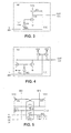
- FIG. 3 illustrates a driver circuit 106 in accordance with one embodiment of the present invention.
- the driver circuit 106 illustrated in FIG. 3 includes an inverter 302 and separate N-type and P-type drive transistors, 304 and 306. Note that separating the final drive transistors avoids crossover current and speeds operation. Note that D[0] and D[1] are different complementary inputs.
- FIG. 4 illustrates a driver circuit in accordance with another embodiment of the present invention.
- each of the drive transistors is split into two parts that are wired in parallel.
- the drivers illustrated in FIGs. 3 and 4 each have two separate inputs, D[0] and D[1]. Making both of these inputs high shuts off the driver. Moreover, only one of the inputs goes low at a given to time to force the driver's output to either high or low. More specifically, if D[0] goes low, the driver's output goes to zero (or low), and if 3[1] goes low, the driver's output goes to one (or high).
- the P-type drive transistor can be 12 microns wide and the N-type drive transistor can be six microns wide.
- the driver illustrated in FIGs. 3 responds quickly to low-going changes at its input.
- the P-type transistor responds as soon as D[1] reaches one threshold voltage lower than V DD .
- the high-threshold inverter in front of the N-type transistor similarly responds soon after D[0] begins to go low.
- the narrowest possible transistors can be chosen that make a high-threshold inverter.
- the N-type is 0.6 microns wide and the P-type is 4 times as wide, or 2.4 microns, or alternatively, the NMOS can be debilitated by increasing its length.
- FIG. 5 illustrates a pass circuit in accordance with an embodiment of the present invention.
- the two inverters X 512 and Y 514 form a keeper circuit that acts as a memory element.
- the two N-type transistors 504 and 510 are pass gates that are driven by clock signal 101. When clock signal 101 goes high, pass transistors 504 and 510 pull down either D[0] or D[1], depending on the value of the input 100.
- the latch illustrated in FIG. 5 shuts off reluctantly.
- the second shutoff mechanism uses the very narrow P-type transistor 506. When clock signal 101 is low, P-type transistor 506 forces an otherwise undriven side high, shutting off the structure completely.
- FIG. 6 illustrates a pass circuit used for rapid shutoff in accordance with another embodiment of the present invention.
- the clock signal 101 drives P-type transistors 602 and 612 that are used for shutoff, as well as the N-type pass transistors 604 and 610.
- clock signal 101 drives P-type transistors 602 and 612 that are used for shutoff, as well as the N-type pass transistors 604 and 610.
- the latch illustrated in FIG. 6 presents more capacitive load to clock signal 101 than the latch illustrated in FIG. 5 in return for a much more rapid shut off.
- FIG. 7 illustrates a pass circuit with an inverting structure in accordance with yet another embodiment of the present invention.
- input 100 enters a domino amplifier rather than a pass gate structure.
- This domino structure can be every bit as fast as the pass gate structure, and has the further advantage of avoiding a current drain on input 100.
- a single N-type transistor 716 can serve both sides of the circuit because only one side draws current at a time.
- the cross-coupling required in the latches illustrated in FIGS. 5 and 8 is absent here because of the logic inversion.
- FIG. 8 illustrates a pass circuit with the keeper omitted in accordance with a further embodiment of the present invention.
- the circuit illustrated in FIG. 8 is used when some other structure provides the keeper function. For example, if one latch drives multiple output latches (as in FIG. 9A), the latch illustrated in FIG. 5 can be used for the first output latch 904, and the latch illustrated in FIG. 8 can be used for the remaining latch 906.
- a particular property of the latches illustrated in FIGS. 5, 7, and 8 is their "reluctant" shut off.
- a second control input can only renew the same output state anyway, so why hasten to shut off the output drive?
- the latches illustrated in FIGs. 5, 7 and 8 avoid loading clock signal 101 in order to shut off their output drive. Instead, they use current from input 100 to shut off whichever output side will not be used in the next cycle.
- FIG. 10 illustrates a latch circuit in accordance with another embodiment of the present invention.
- the latch illustrated in FIG. 10 contains 10 transistors, including transistors for the keeper circuit.
- clock signal 101 is asserted after input 100 changes, there is one gate delay from the assertion of clock signal 101 until a corresponding transition appears at output 108 for a low value and two gate delays for a high value.
- clock signal 101 changes while clock signal 101 is asserted, there are two gate delays until the transition appears at output 108 for both high-going and low-going signals.
- clock signal 101 controls N-type transistor 1012.
- N-type transistor 1012 When N-type transistor 1012 becomes transparent, it sources current through one of two N-type transistors 1004 and 1014 depending upon the value of input 100. If input 100 is high, N-type transistor 1012 delivers current to N-type transistor 1004. The drain of N-type transistor 1004 is coupled to the gate of P-type drive transistor 1016, which pulls output 108 high. If input 100 is low, N-type transistor 1012 delivers current to N-type drive transistor 1014. The drain of N-type drive transistor 1014 is coupled to output 108.
- N-type transistor 1012 ensures that P-type drive transistor 1016 is turned off when clock signal 101 is not asserted.
- P-type transistor 1002 ensures that P-type drive transistor 1016 turns off if input 100 changes from high to low while clock signal 101 is asserted.
- FIG. 11 illustrates a latch circuit in accordance with another embodiment of the present invention.
- the latch illustrated in FIG. 11 is the same as the latch illustrated in FIG. 10 except that an extra stage of gain is added. This extra stage of gain causes the latch to invert.
- the latch illustrated in FIG. 11 operates in the same manner as the latch illustrated in FIG. 10 except for the way P-type transistor 1101 is used. Note that either P-type transistor 1002 or P-type transistor 1102 will be conducting at any given time. P-type transistor 1101 shorts the drains of these two transistors when clock signal 101 is low. This ensures that the drains of both P-type transistors 1002 and 1102 are at a high voltage, which shuts off drive transistors 1016 and 1014.
Landscapes
- Logic Circuits (AREA)
- Synchronisation In Digital Transmission Systems (AREA)
Abstract
Description
Claims (18)
- An apparatus for latching data in response to a clock signal, comprising:a memory element that is configured to store a data value;a latch input coupled to the memory element, whereby changes in the latch input change the data value stored in the memory element without waiting for an assertion of the clock signal;a latch output;a driver circuit that is configured to drive the data value stored in the memory element onto the latch output; anda clocking circuit that is configured to cause the driver circuit to drive the data value stored in memory element onto the latch output in response to an assertion of the clock signal.
- The apparatus of claim 1, wherein the clocking circuit is configured to pass the data value stored in the memory element to the driver circuit in response an assertion of the clock signal in order to drive data value onto the latch output.
- The apparatus of claim 1 or 2, wherein the memory element includes a bistable circuit.
- The apparatus of claim 1 or 2,
wherein the memory element includes a keeper circuit comprising a first inverter and a second inverter;
wherein the first inverter and the second inverter are coupled into a ring, so that the output of the first inverter is coupled to the input of the second inverter and the output of the second inverter is coupled to the input of the first inverter. - The apparatus of claim 1 or 2, wherein the memory element includes a capacitive memory element.
- The apparatus of any preceding claim, wherein the driver circuit includes:a P-type transistor with a source coupled to VDD, a drain coupled to the latch output, and a gate coupled through the clocking circuit to a complement of the data value stored in the memory element; andan N-type transistor with a source coupled to ground, a drain coupled to the latch output, and a gate coupled through the clocking circuit to the data value stored in the memory element.
- The apparatus of any preceding claim, wherein the clocking circuit includes:a first N-type pass transistor, with a drain coupled to the data value stored in the memory element, a source coupled through an inverter to a gate of a P-type transistor within the driver circuit, and a gate coupled to the clock signal; anda second N-type pass transistor, with a drain coupled to a complement of the data value stored in the memory element, a source coupled to a gate of a N-type transistor within the driver circuit, and a gate coupled to the clock signal.
- The apparatus of any of claims 1-6, wherein the clocking circuit includes a domino amplifier that is configured to drive the data value stored in the memory element into the driver circuit when the clock signal is asserted.
- The apparatus of any of claims 1 to 6, wherein the clocking circuit includes an N-type clocking transistor coupled in series with drive transistors in the driver circuit, wherein the gate of the N-type clocking transistor is coupled to the clock signal, so that asserting the clock signal causes the driver circuit to be activated.
- The apparatus of any preceding claim,
wherein the latch input is coupled to the input of a second latch; and
wherein the memory element is shared with second latch and is located at the input of the second latch. - The apparatus of any preceding claim, further comprising a turnoff circuit that is configured to turn off the driver circuit after the data value stored in the memory element has been driven onto the latch output.
- The apparatus of claim 11, wherein the turnoff circuit includes at least one P-type turnoff transistor with a source coupled to VDD, a drain coupled to a gate of a drive transistor within the driver circuit, and a gate coupled to a turnoff signal, so activating the turnoff signal causes the driver circuit to turn off.
- The apparatus of claim 12, wherein the turnoff signal is derived from the latch input.
- The apparatus of claim 12, wherein the turnoff signal is derived from the clock signal.
- An method for latching data in response to a clock signal, comprising:receiving a change in a latch input;in response to the change in the latch input, changing a data value stored in a memory element without waiting for an assertion of the clock signal;receiving an assertion of the clock signal; andin response to the assertion of the clock signal, using a driver circuit to drive the data value stored in the memory element onto a latch output.
- The method of claim 15, further comprising turning off the driver circuit after the data value stored in the memory element has been driven onto the latch output.
- The method of claim 16, wherein turning off the driver circuit involves using the latch input to turn off the driver circuit.
- The method of claim 16, wherein turning off the driver circuit involves using the clock signal to turn off the driver circuit.
Applications Claiming Priority (2)
| Application Number | Priority Date | Filing Date | Title |
|---|---|---|---|
| US09/834,772 US6456136B1 (en) | 2001-04-13 | 2001-04-13 | Method and apparatus for latching data within a digital system |
| US834772 | 2001-04-13 |
Publications (2)
| Publication Number | Publication Date |
|---|---|
| EP1249935A2 true EP1249935A2 (en) | 2002-10-16 |
| EP1249935A3 EP1249935A3 (en) | 2005-03-16 |
Family
ID=25267767
Family Applications (1)
| Application Number | Title | Priority Date | Filing Date |
|---|---|---|---|
| EP02252268A Withdrawn EP1249935A3 (en) | 2001-04-13 | 2002-03-27 | Method and apparatus for latching data within a digital system |
Country Status (2)
| Country | Link |
|---|---|
| US (1) | US6456136B1 (en) |
| EP (1) | EP1249935A3 (en) |
Families Citing this family (5)
| Publication number | Priority date | Publication date | Assignee | Title |
|---|---|---|---|---|
| WO2002045196A2 (en) * | 2000-11-30 | 2002-06-06 | Mti Microfuel Cells, Inc. | Fuel cell membrane and system with integrated gas separation |
| US6762957B2 (en) | 2001-12-20 | 2004-07-13 | Intel Corporation | Low clock swing latch for dual-supply voltage design |
| US6563357B1 (en) * | 2001-12-20 | 2003-05-13 | Intel Corporation | Level converting latch |
| US7502507B2 (en) * | 2002-10-31 | 2009-03-10 | Microsoft Corporation | Active embedded interaction code |
| US7671653B2 (en) * | 2007-09-28 | 2010-03-02 | Sun Microsystems, Inc. | Dual edge triggered flip flops |
Family Cites Families (9)
| Publication number | Priority date | Publication date | Assignee | Title |
|---|---|---|---|---|
| US4138613A (en) * | 1974-08-14 | 1979-02-06 | Kabushiki Kaisha Daini Seikosha | Switching circuit |
| US4484087A (en) * | 1983-03-23 | 1984-11-20 | General Electric Company | CMOS latch cell including five transistors, and static flip-flops employing the cell |
| US4914318A (en) * | 1988-12-30 | 1990-04-03 | Intel Corporation | Latch circuit for a programmable logic device using dual n-type transistors |
| JP2621993B2 (en) * | 1989-09-05 | 1997-06-18 | 株式会社東芝 | Flip-flop circuit |
| GB2292855A (en) * | 1994-08-31 | 1996-03-06 | Texas Instruments Ltd | CMOS latch suitable for low voltage operation |
| US5719516A (en) * | 1995-12-20 | 1998-02-17 | Advanced Micro Devices, Inc. | Lock generator circuit for use with a dual edge register that provides a separate enable for each use of an input clock signal |
| KR100244456B1 (en) * | 1997-03-22 | 2000-02-01 | 김영환 | Clock control device for data output buffer |
| US5870331A (en) * | 1997-09-26 | 1999-02-09 | Advanced Micro Devices, Inc. | Application-specific SRAM memory cell for low voltage, high speed operation |
| JPH11203864A (en) * | 1998-01-14 | 1999-07-30 | Mitsubishi Electric Corp | Synchronous semiconductor memory device |
-
2001
- 2001-04-13 US US09/834,772 patent/US6456136B1/en not_active Expired - Lifetime
-
2002
- 2002-03-27 EP EP02252268A patent/EP1249935A3/en not_active Withdrawn
Also Published As
| Publication number | Publication date |
|---|---|
| EP1249935A3 (en) | 2005-03-16 |
| US6456136B1 (en) | 2002-09-24 |
| US20020149410A1 (en) | 2002-10-17 |
Similar Documents
| Publication | Publication Date | Title |
|---|---|---|
| EP0690577B1 (en) | CMOS integrated circuit for fast propagation of a signal edge | |
| US6282133B1 (en) | Semiconductor memory device having a delay circuit for generating a read timing | |
| US7489165B2 (en) | Method and apparatus for amplifying a regulated differential signal to a higher voltage | |
| US6231147B1 (en) | Data storage circuits using a low threshold voltage output enable circuit | |
| US6919735B2 (en) | Skewed nor and nand rising logic devices for rapidly propagating a rising edge of an output signal | |
| US5396108A (en) | Latch controlled output driver | |
| EP1173924A1 (en) | Fast high voltage level shifter with gate oxide protection | |
| US7365575B2 (en) | Gated clock logic circuit | |
| JP2003516016A (en) | Voltage conversion circuit | |
| US5825225A (en) | Boosted differential latch | |
| US5424653A (en) | Gradual on output buffer circuit including a reverse turn-off apparatus | |
| JP2733578B2 (en) | CMOS latch circuit | |
| US6456136B1 (en) | Method and apparatus for latching data within a digital system | |
| US6380781B1 (en) | Soft error rate tolerant latch | |
| US7449924B2 (en) | Latch-based serial port output buffer | |
| US6348824B1 (en) | High speed static latch | |
| KR100311973B1 (en) | Logic interface circuit and semiconductor memory device using this circuit | |
| EP0487911A2 (en) | A fast cycle time clocked amplifier | |
| US5394363A (en) | Pulse write driver circuit | |
| US7149128B2 (en) | Data latch | |
| US6411553B1 (en) | Single ended data bus equilibration scheme | |
| US6507222B1 (en) | High speed single ended sense amplifier | |
| JP4386523B2 (en) | Dynamic logic circuit | |
| EP0614293B1 (en) | Multiplexer | |
| JP3016985B2 (en) | Semiconductor storage device |
Legal Events
| Date | Code | Title | Description |
|---|---|---|---|
| PUAI | Public reference made under article 153(3) epc to a published international application that has entered the european phase |
Free format text: ORIGINAL CODE: 0009012 |
|
| AK | Designated contracting states |
Kind code of ref document: A2 Designated state(s): AT BE CH CY DE DK ES FI FR GB GR IE IT LI LU MC NL PT SE TR |
|
| AX | Request for extension of the european patent |
Free format text: AL;LT;LV;MK;RO;SI |
|
| RAP1 | Party data changed (applicant data changed or rights of an application transferred) |
Owner name: SUN MICROSYSTEMS, INC. |
|
| PUAL | Search report despatched |
Free format text: ORIGINAL CODE: 0009013 |
|
| AK | Designated contracting states |
Kind code of ref document: A3 Designated state(s): AT BE CH CY DE DK ES FI FR GB GR IE IT LI LU MC NL PT SE TR |
|
| AX | Request for extension of the european patent |
Extension state: AL LT LV MK RO SI |
|
| 17P | Request for examination filed |
Effective date: 20050830 |
|
| AKX | Designation fees paid |
Designated state(s): DE FR GB |
|
| STAA | Information on the status of an ep patent application or granted ep patent |
Free format text: STATUS: THE APPLICATION IS DEEMED TO BE WITHDRAWN |
|
| 18D | Application deemed to be withdrawn |
Effective date: 20060613 |