EP1248378A1 - Transmitter and radio communication terminal using the same - Google Patents
Transmitter and radio communication terminal using the same Download PDFInfo
- Publication number
- EP1248378A1 EP1248378A1 EP00900166A EP00900166A EP1248378A1 EP 1248378 A1 EP1248378 A1 EP 1248378A1 EP 00900166 A EP00900166 A EP 00900166A EP 00900166 A EP00900166 A EP 00900166A EP 1248378 A1 EP1248378 A1 EP 1248378A1
- Authority
- EP
- European Patent Office
- Prior art keywords
- frequency
- signal
- output
- counter
- output signal
- Prior art date
- Legal status (The legal status is an assumption and is not a legal conclusion. Google has not performed a legal analysis and makes no representation as to the accuracy of the status listed.)
- Granted
Links
Images


Classifications
-
- H—ELECTRICITY
- H03—ELECTRONIC CIRCUITRY
- H03C—MODULATION
- H03C3/00—Angle modulation
- H03C3/02—Details
- H03C3/09—Modifications of modulator for regulating the mean frequency
- H03C3/0908—Modifications of modulator for regulating the mean frequency using a phase locked loop
- H03C3/0983—Modifications of modulator for regulating the mean frequency using a phase locked loop containing in the loop a mixer other than for phase detection
-
- H—ELECTRICITY
- H03—ELECTRONIC CIRCUITRY
- H03C—MODULATION
- H03C3/00—Angle modulation
- H03C3/02—Details
- H03C3/09—Modifications of modulator for regulating the mean frequency
- H03C3/0908—Modifications of modulator for regulating the mean frequency using a phase locked loop
- H03C3/0916—Modifications of modulator for regulating the mean frequency using a phase locked loop with frequency divider or counter in the loop
- H03C3/0925—Modifications of modulator for regulating the mean frequency using a phase locked loop with frequency divider or counter in the loop applying frequency modulation at the divider in the feedback loop
-
- H—ELECTRICITY
- H03—ELECTRONIC CIRCUITRY
- H03C—MODULATION
- H03C3/00—Angle modulation
- H03C3/02—Details
- H03C3/09—Modifications of modulator for regulating the mean frequency
- H03C3/0908—Modifications of modulator for regulating the mean frequency using a phase locked loop
- H03C3/0966—Modifications of modulator for regulating the mean frequency using a phase locked loop modulating the reference clock
-
- H—ELECTRICITY
- H03—ELECTRONIC CIRCUITRY
- H03D—DEMODULATION OR TRANSFERENCE OF MODULATION FROM ONE CARRIER TO ANOTHER
- H03D7/00—Transference of modulation from one carrier to another, e.g. frequency-changing
- H03D7/16—Multiple-frequency-changing
- H03D7/161—Multiple-frequency-changing all the frequency changers being connected in cascade
- H03D7/163—Multiple-frequency-changing all the frequency changers being connected in cascade the local oscillations of at least two of the frequency changers being derived from a single oscillator
-
- H—ELECTRICITY
- H03—ELECTRONIC CIRCUITRY
- H03L—AUTOMATIC CONTROL, STARTING, SYNCHRONISATION OR STABILISATION OF GENERATORS OF ELECTRONIC OSCILLATIONS OR PULSES
- H03L7/00—Automatic control of frequency or phase; Synchronisation
- H03L7/06—Automatic control of frequency or phase; Synchronisation using a reference signal applied to a frequency- or phase-locked loop
- H03L7/16—Indirect frequency synthesis, i.e. generating a desired one of a number of predetermined frequencies using a frequency- or phase-locked loop
- H03L7/22—Indirect frequency synthesis, i.e. generating a desired one of a number of predetermined frequencies using a frequency- or phase-locked loop using more than one loop
- H03L7/23—Indirect frequency synthesis, i.e. generating a desired one of a number of predetermined frequencies using a frequency- or phase-locked loop using more than one loop with pulse counters or frequency dividers
-
- H—ELECTRICITY
- H04—ELECTRIC COMMUNICATION TECHNIQUE
- H04B—TRANSMISSION
- H04B1/00—Details of transmission systems, not covered by a single one of groups H04B3/00 - H04B13/00; Details of transmission systems not characterised by the medium used for transmission
- H04B1/02—Transmitters
- H04B1/04—Circuits
- H04B1/0475—Circuits with means for limiting noise, interference or distortion
-
- H—ELECTRICITY
- H04—ELECTRIC COMMUNICATION TECHNIQUE
- H04L—TRANSMISSION OF DIGITAL INFORMATION, e.g. TELEGRAPHIC COMMUNICATION
- H04L25/00—Baseband systems
- H04L25/02—Details ; arrangements for supplying electrical power along data transmission lines
- H04L25/03—Shaping networks in transmitter or receiver, e.g. adaptive shaping networks
- H04L25/03006—Arrangements for removing intersymbol interference
- H04L25/03343—Arrangements at the transmitter end
-
- H—ELECTRICITY
- H03—ELECTRONIC CIRCUITRY
- H03J—TUNING RESONANT CIRCUITS; SELECTING RESONANT CIRCUITS
- H03J2200/00—Indexing scheme relating to tuning resonant circuits and selecting resonant circuits
- H03J2200/17—Elimination of interference caused by harmonics of local oscillator
-
- H—ELECTRICITY
- H04—ELECTRIC COMMUNICATION TECHNIQUE
- H04B—TRANSMISSION
- H04B1/00—Details of transmission systems, not covered by a single one of groups H04B3/00 - H04B13/00; Details of transmission systems not characterised by the medium used for transmission
- H04B1/02—Transmitters
- H04B1/04—Circuits
- H04B2001/0491—Circuits with frequency synthesizers, frequency converters or modulators
Definitions
- the present invention relates to a transmitter including a frequency synthesizer and a PLL frequency conversion circuit and to a wireless communication terminal apparatus using the same used in a wireless communication system such as the GSM, the DCS1800, or the like.
- the following three types are considered as a configuration of a transmitter used in a wireless communication terminal apparatus.
- the architecture (3) since only a constant envelope modulation can be handled as a modulation architecture, architectures (1) and (2) have been mainstream as the architecture of the transmitter.
- the architecture (3) having various advantages has been started to widely use.
- the advantages of the architecture (3) include: (1) that an expensive filter having a high Q value is not required in the transmitter according to filter characteristics which the PLL has, (2) that, since a VCO output signal is a constant envelope signal, a bias design of a power amplifier at the next stage of the PLL frequency conversion circuit becomes easy, and the like.
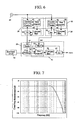
- FIG. 6 shows a transmitter of the architecture (3) according to a comparative example which is an assumption of the present invention.
- This transmitter is configured with a first frequency synthesizer 38, a second frequency synthesizer 39, a crystal oscillator 40 for giving reference signals to the first and second frequency synthesizers, a PLL frequency conversion circuit 41, a divider 47, a modulator 54, and a base band circuit 42.
- the first frequency synthesizer 38 is configured with a first counter 42, a second counter 43, a phase comparator 44, a low pass filter 45, and a VCO 46, where an output signal of the VCO 46 is input into the divider 47.
- the second frequency synthesizer 39 is configured with a third counter 48, a fourth counter 49, a phase comparator 50, a low pass filter 51, and a VCO 52, where an output signal of the VCO 52 which is a frequency fRF is input into a mixer 53.
- the base band circuit 42 is a circuit for generating a waveform of a base band signal or generating various data for controlling this transmitter.
- the divider 47 divides this local signal into a frequency fIF, and inputs it into the modulator 54.
- the modulator 54 mixes the signal of the frequency fIF supplied from the divider 47 into a base band signal from the base band circuit 42, and upconverts it to an intermediate frequency (for example, 270 MHz).
- an intermediate frequency for example, 270 MHz.
- the PLL frequency conversion circuit 41 is configured with a phase comparator 55, a low pass filter 56, a VCO 57, and the mixer 53. Two signals are input into the phase comparator 55. A first input signal is an output signal of the modulator 54, and a second input signal is an output signal of the mixer 53. In the phase comparator 55, the first and second input signals are phase-compared with each other, and a signal proportional to a phase difference is output. The output signal of the phase comparator 55 is output to the low pass filter 56, where undesired noises are eliminated, and is then input into the VCO 57. The output frequency of the VCO 57 is an fVCO, which is used as an output signal of this transmitter and is input into the mixer 53.
- a first input signal is an output signal of the VCO 57
- a second input signal is a local signal of the frequency fRF supplied from the second frequency synthesizer 39.
- the output frequency of the mixer 53 is an absolute value of a difference between the two input frequencies, which becomes
- the output frequency fRF of the second frequency synthesizer 39 is changed while the output frequency of the first frequency synthesizer 38 remains fixed.
- FIG. 7 An example of closed-loop characteristics of the PLL frequency conversion circuit 41 is shown in FIG. 7.
- a flat portion of 0 dB is a bandpass. Since the frequency of the horizontal axis denotes a offset frequency from the output frequency fVCO, it is found that the PLL frequency conversion circuit 41 has bandpass filter characteristics around the output frequency.
- the bandpass width is set to be wider than the bandwidth in the modulation architecture prescribed in the system such as the GSM or the like, the PLL frequency conversion circuit 41 can hold an output spectrum of the modulator 54, and convert the center frequency.
- the bandpass width is designed to be about 1 to 2 MHz.
- Needs for low cost, small capacity, and the like have been remarkably required for the wireless communication terminal apparatus, and an integration of a circuit structuring a terminal has been advanced year after year.
- a problem of a crosstalk of signals or harmonics between circuits has occurred along with an enhancement of the integration.
- an improvement of a semiconductor process in recent years is being advanced in a direction of decreasing a parasitic capacitance, which also promotes the problem of the crosstalk between circuits.
- a problem of the crosstalk through a mounting substrate has occurred due to a high density mounting such as an IC in a terminal.
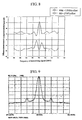
- FIG. 8 shows measurement results of the transmitter in which circuits surrounded by solid lines 58 and 59 in FIG. 6 are integrated in the same IC.
- the GSM is assumed as the system, and a GMSK modulation signal is used as the base band signal.
- the horizontal axis denotes the transmission frequency fVCO of the transmitter, and the vertical axis denotes a worst value of a difference between a signal level at the transmission frequency and a signal level at 400 MHz to 1.8 MHz offset and 6 MHz to 25 MHz offset from the transmission frequency by dB.
- the specifications with respect to Spurious emissions of the GSM are not more than -60 dB and not more than -71 dB at 400 kHz to 1.8 MHz offset and at not less than 6 MHz offset, respectively.
- the transmission frequency is in the vicinity of 900 MHz at 400 kHz to 1.8 MHz offset, it is found that, when the transmission frequency is in the vicinity of 898 MHz and in the vicinity of 902 MHz at 6 MHz to 25 MHz offset, the transmission spectrum is degraded, which does not meet the GSM specification. This is because undesired spurs occur in the offset frequency shown in formula 1 from the transmission frequency due to an intermodulation of harmonics of the fIF, the fRF and the fVCO.
- FIG. 9 shows an output spectrum of the transmitter in which the circuits surrounded by the solid lines 58 and 59 and the VCO 46 in FIG. 6 are integrated in the same IC.
- the GSM is assumed as the system, and the GMSK modulation signal is used as the base band signal.
- the first frequency synthesizer 38 oscillates at 1080 MHz, and is quadrant divided in the divider 47, where the fIF is assumed to be 270 MHz.
- the fRF is set at 1150 MHz so that the fVCO becomes 880 MHz.
- the output frequency of the crystal oscillator 40 is 13 MHz.
- the horizontal axis denotes a frequency
- the vertical axis denotes a signal level by dBm.
- the undesired spurs occur at 1 MHz offset from the transmission frequency, and the level thereof is -58.2 dB. As described above, in the GSM specification, the level is prescribed to be not more than -60 dB at 400 kMz to 1.8 MHz offset, and the measurement result in FIG. 9 does not meet the GSM specification.
- the occurrence process of the undesired spurs is as follows. Harmonics of 1079 MHz which is 83 times the output signal of the crystal oscillator 40 occur in the first frequency synthesizer 38 or the second frequency synthesizer 39. This 1079 MHz signal is mixed into the VCO 46 due to the crosstalk.
- the transmitter according to the aforementioned comparative example has the problems of the undesired spurs described later due to a progress of the integration of a circuit, a deterioration of the parasitic capacitance due to the improvement of the semiconductor process, or the high density mounting of a terminal.
- a first problem (1) is in that the undesired spurs occur at a specific transmission frequency due to the harmonics of the output signal of the frequency synthesizer.
- a second problem (2) is in that, when the harmonics of the output signal of the crystal oscillator are present in the vicinity of the oscillation frequency of the VCO, the undesired spurs occur in the VCO output due to the folded operation of the VCO.
- a transmitter is a transmitter comprising a first frequency synthesizer; a second frequency synthesizer; a base band circuit for outputting a base band signal and a control signal on the basis of an information signal; a control circuit for changing output frequencies of the first frequency synthesizer and the second frequency synthesizer on the basis of the control signal; a modulator for assuming an output signal from the first frequency synthesizer to be a carrier signal and modulating the carrier signal on the basis of the base band signal; and a frequency conversion circuit for using an output signal form the modulator and an output signal from the second frequency synthesizer to upconvert a carrier frequency of the output signal from the modulator.
- the frequency conversion circuit is a PLL frequency conversion circuit comprising a first phase comparator; a first low pass filter; a first VCO; and a mixer; wherein the first phase comparator outputs a signal proportional to a phase difference between an output signal from the modulator and an output signal from the mixer; the first low pass filter is connected to an output of the first phase comparator; the first VCO is connected to an output of the first low pass filter; and the mixer is adopted to mix an output signal from the first VCO and an output signal from the second frequency synthesizer.
- the base band circuit is a base band circuit which stores a relationship between an output frequency of the frequency conversion circuit and output frequencies of the first frequency synthesizer and the second frequency synthesizer and generates the control signal corresponding to the output frequency of the frequency conversion circuit on the basis of the relationship.
- the relationship is a relationship where undesired spurs equal to or more than a level prescribed in a wireless system do not occur in an output of the PLL frequency conversion circuit.
- the first frequency synthesizer comprises a first counter; a second counter; a second phase comparator; a second low pass filter; and a second VCO; wherein the second phase comparator outputs a signal proportional to a phase difference between an output signal from the first counter and an output signal from the second counter; the first counter is connected to an output of a reference oscillator; the second counter is connected to an output of the second VCO; the second low pass filter is connected to an output of the second phase comparator; the second VCO is connected to an output of the second low pass filter; and a frequency ratio of the second counter can be changed by first frequency ratio data transmitted from the control circuit.
- the second frequency synthesizer comprises a third counter; a fourth counter; a third phase comparator; a third low pass filter; and a third VCO, wherein the third phase comparator outputs a signal proportional to a phase difference between an output signal from the third counter and an output signal from the fourth counter; the third counter is connected to an output of the reference oscillator; the fourth counter is connected to an output of the third VCO; the third low pass filter is connected to an output of the third phase comparator; the third VCO is connected to an output of the third low pass filter; and a frequency ratio of the fourth counter can be changed by second frequency ratio data transmitted from the control circuit.
- control circuit comprises a first register for holding third frequency ratio data; a second register for holding fourth frequency ratio data; a third register for holding the second frequency ratio data; and a first selector for selecting either one item of the third and fourth frequency ratio data on the basis of information included in the control signal and assuming it to be the first frequency ratio data.
- a divider may exist between the second VCO and the modulator.
- the first counter, the second counter, the second phase comparator, the third counter, the fourth counter, the third phase comparator, the modulator, the divider, the first phase comparator, the mixer, and the control circuit are formed in the same IC.
- a transmitter is the transmitter wherein the control circuit comprises a fourth register for holding fifth frequency ratio data; a fifth register for holding sixth frequency ratio data; a sixth register for holding the seventh frequency ratio data; a seventh register for holding the second frequency ratio data; and a second selector for selecting one item of the fifth, sixth, and seventh frequency ratio data on the basis of information included in the control signal and assuming it to be the first frequency ratio data.
- a divider may be exist between the second VCO and the modulator.
- At least the first counter, the second counter, the second phase comparator, the third counter, the fourth counter, the third phase comparator, and the second VCO are manufactured in the same IC, preferably, the modulator, the divider, the first phase comparator, the mixer, and the control circuit are further formed in the same IC.
- a wireless communication terminal apparatus is a wireless communication terminal apparatus comprising a base band circuit for outputting a base band signal and a control signal on the basis of an information signal; a transmitting circuit to which the base band signal and the control signal are input; the receiving circuit to which a first output signal and a second output signal from the transmitting circuit are input; a power amplifier to which a third output signal from the transmitting circuit is input, an antenna switch connected to an input of the receiving circuit and to an output of the power amplifier; and an antenna connected to the antenna switch, wherein the transmitting circuit is a transmitter according to any one of the above aspects; the first output signal and the second output signal are an output signal from a second frequency synthesizer and an input signal to a modulator both in the transmitting circuit; the third output signal is an output signal from a first VCO provided in the transmitting circuit; and an output signal of the receiving circuit is input into the base band circuit in the transmitting circuit, where an information signal is fetched out.
- a duplexer may be employed in place of the antenna switch.
- the output frequency of the frequency synthesizer is appropriately changed according to the output frequency of the PLL frequency conversion circuit so that the undesired spurs can be suppressed.
- FIG. 1 is a configuration diagram showing a first embodiment of a transmitter according to the present invention, which solves the first object (1).
- the transmitter according to the present invention is configured with a first frequency synthesizer 1, a second frequency synthesizer 2, a crystal oscillator 3 for giving reference signals to the first and second frequency synthesizers 1 and 2, a control circuit 4 for the first and second frequency synthesizers 1 and 2, a PLL frequency conversion circuit 5, a divider 12, a modulator 18, and a base band circuit 6.
- the first frequency synthesizer 1 is configured with a first counter 7, a second counter 8, a phase comparator 9, a low pass filter 10, and a VCO 11, where an output signal of the VCO 11 is input into the divider 12.
- the second frequency synthesizer 2 is configured with a third counter 12, a fourth counter 13, a phase comparator 14, a low pass filter 15, and a VCO 16, where an output signal of the VCO 16 which is a frequency fRF is input into a mixer 17.
- the base band circuit 6 is a circuit for generating a waveform of a base band signal or generating various data for controlling the transmitter.
- the control circuit 4 is configured with a first register 22, a second register 23, a third register 24, a fourth register 25, a decoder 26, and a selector 27.
- a clock signal CLK and a data signal DATA are input into the first register 22 from the base band circuit 6, where this DATA is synchronized with this CLK and is stored as serial data.
- Part of the stored data (for example, higher 3 bits) is input into the decoder 26, and the remaining thereof is input into the second, third and fourth registers 23, 24, and 25.
- Data from the first register 22 is stored only in one register selected from among the second, third, and fourth registers 23, 24 and 25 by the output signal of the decoder 26.
- a timing with which the data is stored is determined by a trigger signal (for example, a fall edge) transmitted to the LE.
- the outputs of the second and third registers 23 and 24 are input into the selector 27.
- the selector 27 inputs either one of the outputs from the second and third registers 23 and 24 into the counter 8 according to selector data 28 from the fourth register 25.
- Part of the data (for example, higher 1 bit) stored in the fourth register 25 is output to the selector 27, and the remaining thereof is input into the counter 13 of the second frequency synthesizer 2.
- the divider 12 divides this local signal into a frequency fIF, and inputs it into the modulator 18.
- the modulator 18 mixes a signal of the frequency fIF supplied from the divider 12 into the base band signal from the base band circuit 6, and upconverts it to an intermediate frequency (for example, 270 MHz).
- the PLL frequency conversion circuit 5 is configured with a phase comparator 19, a low pass filter 20, a VCO 21, and a mixer 17. Two signals are input into the phase comparator 19. A first input signal is an output signal of the modulator 18, and a second input signal is an output signal of the mixer 17. In the phase comparator 19, the first and second input signals are phase-compared with each other, and a signal proportional to a phase difference is output. The output signal of the phase comparator 19 is output to the low pass filter 20, where undesired noises are eliminated, and is input into the VCO 21. An output frequency of the VCO 21 is an fVCO, which is used as an output signal of this transmitter and is input into the mixer 17. Two signals are input into the mixer 17.
- a first input signal is an output signal of the VCO 21, and a second input signal is a signal of the frequency fRF supplied from the second frequency synthesizer 2.
- the output frequency of the mixer 17 is an absolute value of a difference between the two input frequencies, which is
- the output signal of the mixer 17 becomes the second input signal of the phase comparator 19.
- a frequency conversion operation and an operation as a bandpass filter of the PLL frequency conversion circuit 5 are similar to a PLL frequency conversion circuit shown in a comparative example which is an assumption of the present invention.
- circuits surrounded by a solid line 29 in FIG. 1 are incorporated in a single IC.
- this transmitter At first, at an initial operation of this transmitter (for example, when a power supply is turned from OFF to ON), the data is stored in the second register 23, and the data is next stored in the third register 24. For example, the data of the counter 8 where the fIF becomes 270 MHz is stored in the second register 23, and the data of the counter 8 where the fIF becomes 272 MHz is stored in the third register 24. Once the data are stored in the second and third registers 23 and 24, updating of the data will not be performed thereafter.
- the data is input into the fourth register 25 and the data of the counter 13 is updated in each case so that the output frequency fRF of the second frequency synthesizer 2 is updated, and, at the same time, the selector data 28 is given to the selector 27 so that a value of the second or third register 23 or 24 is input into the counter 8 and the output frequency of the first frequency synthesizer 1 is updated.
- the undesired spurs have occurred with an offset frequency prescribed by formula 1.
- the undesired spurs occur with ⁇ 6 MHz offset.
- the PLL frequency conversion circuit 5 has bandpass filter characteristics with a transmission frequency as a center frequency, a level of the undesired spurs can be suppressed by increasing the offset frequency of the undesired spurs.
- the offset frequency of the undesired spurs becomes ⁇ 26 MHz offset from formula 1.
- the GSM specification can be met in all the frequency ranges.
- FIG. 3 is a configuration diagram showing a second embodiment of the transmitter according to the present invention, which simultaneously solves the first problem (1) and the second problem (2).
- the present embodiment is a transmitter characterized in that the VCO 11 is added to a IC circuit (portion surrounded by a dotted line 29) and further a fifth register 30 is added between the first register 22 and the selector 27 in the first embodiment. Circuits surrounded by a solid line 31 are incorporated in a single IC.
- the undesired spurs are suppressed as compared with the comparative example, the level thereof is -66.4 dB. This value meets not more than -60 dB of the GSM specification.
- the transmitter according to the present embodiment will be used as follows.
- the fIF to be used is, for example, 270 MHz, 272 MHz, and 268 MHz.
- the output frequency of the first frequency synthesizer 1 is made far from 1079 MHz, and is assumed to be 1088 MHz.
- 272 MHz is used as the fIF.
- 268 MHz is also used as the fIF in order to shift the output frequency fVCO of the transmitter at which the undesired spurs occur.
- the fIF of 270 MHz is used for a receiver utilizing the output signals of the first frequency synthesizer 1 and the second frequency synthesizer 2.
- this transmitter for example, the power supply is turned from OFF to ON
- the data of the counter 8 where the fIF becomes 270 MHz is stored in the second register 23
- the data of the counter 8 where the fIF becomes 272 MHz is stored in the third register 24
- the data of the counter 8 where the fIF becomes 268 MHz is stored in the fifth register 30.
- the selector 27 is appropriately switched according to the transmission frequency fVCO, and the data of this third or fifth register 24 or 30 is input into the counter 8.
- the second register 23 is selected by the selector 27, and the data thereof is input into the counter 8.
- FIG. 5 is a diagram showing the embodiment of the wireless communication terminal apparatus using the transmitter according to the present invention.
- the wireless communication terminal apparatus is configured with the base band circuit 6, a transmitting circuit 33, a power amplifier 34, an antenna switch 35, an antenna 36, a receiving circuit 37, and the crystal oscillator 3.
- the transmitting circuit 33 is configured with the first frequency synthesizer 1, the second frequency synthesizer 2, the PLL frequency conversion circuit 5, the divider 12, the modulator 18, and the control circuit 4 in FIG. 1, where the circuits surrounded by the solid line 29 are incorporated in a single IC.
- the transmitting circuit 33 is configured with the first frequency synthesizer 1, the second frequency synthesizer 2, the PLL frequency conversion circuit 5, the divider 12, the modulator 18, and the control circuit 4 in FIG. 3, where the circuits surrounded by the solid line 31 are incorporated in a single IC.
- the clock signal CLK, the data signal DATA, the trigger signal LE, and a base band signal 32 are input from the base band circuit 6 into the transmitting circuit 3.
- the output signal from the crystal oscillator 3 is input into the transmitting circuit 33 and used as reference signals for the first frequency synthesizer 1 and the second frequency synthesizer 2 both provided in the transmitting circuit 33.
- a first output signal is an output signal from the PLL frequency conversion circuit 5, and the frequency thereof is the fVCO.
- a second output signal is an output signal from the divider 12, and the frequency thereof is the fIF.
- a third output signal is an output signal from the second frequency synthesizer 2, and the frequency thereof is the fRF.
- the first output signal from the transmitting circuit 33 is input into the power amplifier 34, where the power is amplified.
- the output signal from the power amplifier 34 is input into the antenna switch 35.
- the antenna 36, an output of the transmitting circuit 33, and an input of the receiving circuit 37 are connected to the antenna switch 35.
- the antenna 36 and the output of the transmitting circuit 33 are electrically connected on the transmission, and the antenna 36 and the input of the receiving circuit 37 are electrically connected on the reception.
- a duplexer may be employed in place of the antenna switch 35.
- a receiving signal received in the antenna 36 is input into the receiving circuit 37 through the antenna switch 35.
- the receiving circuit 37 uses the second and third output signals of the transmitting circuit 33 to downconvert this receiving signal up to the frequency which can be processed in the base band circuit 6 and to input it into the base band circuit 6.
- the circuits structuring the receiving circuit 37 may be manufactured in another IC from the IC structuring the transmitting circuit 33, further at least one circuit structuring the receiving circuit 37 may be incorporated in this IC.
- the transmitter according to the present invention is useful for a transmitter including a frequency synthesizer and a PLL frequency conversion circuit, and can be widely used in a wireless communication terminal apparatus using this transmitter, and the like, used in a wireless communication system such as the GSM, the DCS1800, or the like.
Landscapes
- Engineering & Computer Science (AREA)
- Power Engineering (AREA)
- Computer Networks & Wireless Communication (AREA)
- Signal Processing (AREA)
- Transmitters (AREA)
- Stabilization Of Oscillater, Synchronisation, Frequency Synthesizers (AREA)
- Digital Transmission Methods That Use Modulated Carrier Waves (AREA)
Abstract
Description
Claims (13)
- A transmitter comprising a first frequency synthesizer; a second frequency synthesizer; a base band circuit for outputting a base band signal and a control signal on the basis of an information signal; a control circuit for changing output frequencies of the first frequency synthesizer and the second frequency synthesizer on the basis of the control signal; a modulator for assuming an output signal from the first frequency synthesizer to be a carrier signal and modulating the carrier signal on the basis of the base band signal; and a frequency conversion circuit for using an output signal from the modulator and an output signal from the second frequency synthesizer to upconvert a carrier frequency of the output signal from the modulator.
- A transmitter comprising a first frequency synthesizer; a second frequency synthesizer; a base band circuit for outputting a base band signal and a control signal on the basis of an information signal; a control circuit for changing output frequencies of the first frequency synthesizer and the second frequency synthesizer on the basis of the control signal; a divider for dividing an output signal from the first frequency synthesizer; a modulator for assuming an output signal from the divider to be a carrier signal and modulating the carrier signal on the basis of the base band signal; and a frequency conversion circuit for using an output signal from the modulator and an output signal from the second frequency synthesizer to upconvert a carrier frequency of the output signal from the modulator.
- A transmitter according to claim 1 or 2, wherein the frequency conversion circuit comprises a first phase comparator; a first low pass filter; a first VCO; and a mixer, and the frequency conversion circuit is a PLL frequency conversion circuit in which the first phase comparator outputs a signal proportional to a phase difference between an output signal from the modulator and an output signal from the mixer; the first low pass filter is connected to an output of the first phase comparator; the first VCO is connected to an output of the first low pass filter; and the mixer is adopted to mix an output signal from the first VCO and an output signal from the second frequency synthesizer.
- A transmitter according to claim 3, wherein the base band circuit stores a relationship between an output frequency of the frequency conversion circuit and output frequencies of the first frequency synthesizer and the second frequency synthesizer; and generates the control signal corresponding to the output frequency of the frequency conversion circuit on the basis of the relationship.
- A transmitter according to claim 4, wherein the first frequency synthesizer comprises a first counter; a second counter; a second phase comparator; a second low pass filter; and a second VCO, in which the second phase comparator outputs a signal proportional to a phase difference between an output signal from the first counter and an output signal from the second counter; the first counter is connected to an output of a reference oscillator; the second counter is connected to an output of the second VCO; the second low pass filter is connected to an output of the second phase comparator; the second VCO is connected to an output of the second low pass filter; and a frequency ratio of the second counter can be changed by first frequency ratio data transmitted from the control circuit.
- A transmitter according to claim 5, wherein the second frequency synthesizer comprises a third counter; a fourth counter; a third phase comparator; a third low pass filter; and a third VCO, in which the third phase comparator outputs a signal proportional to a phase difference between an output signal from the third counter and an output signal from the fourth counter; the third counter is connected to an output of the reference oscillator; the fourth counter is connected to an output of the third VCO; the third low pass filter is connected to an output of the third phase comparator; the third VCO is connected to an output of the third low pass filter; and a frequency ratio of the fourth counter can be changed by second frequency ratio data transmitted from the control circuit.
- A transmitter according to claim 6, wherein the control circuit comprises a first register for holding third frequency ratio data; a second register for holding fourth frequency ratio data; a third register for holding the second frequency ratio data; and a first selector for selecting either one item of the third and fourth frequency ratio data on the basis of information included in the control signal to assume it to be the first frequency ratio data.
- A transmitter according to claim 7, wherein the first counter, the second counter, the second phase comparator, the third counter, the fourth counter, the third phase comparator, the modulator, the divider, the first phase comparator, the mixer, and the control circuit are formed in the same IC.
- A transmitter according to claim 6, wherein the control circuit comprises a fourth register for holding fifth frequency ratio data; a fifth register for holding sixth frequency ratio data; a sixth register for holding the seventh frequency ratio data; a seventh register for holding the second frequency ratio data; and a second selector for selecting one item of the fifth, sixth, and seventh frequency ratio data on the basis of information included in the control signal to assume it to be the first frequency ratio data.
- A transmitter according to claim 9, wherein at least the first counter, the second counter, the second phase comparator, the third counter, the fourth counter, the third phase comparator, and the second VCO are formed in the same IC.
- A transmitter according to claim 10, wherein the modulator, the divider, the first phase comparator, the mixer, and the control circuit are further formed in the same IC.
- A wireless communication terminal apparatus using a transmitter according to claim 1, 2, 3, 4, 5, 6, 7, 8, 9, 10, or 11, comprising a transmitting circuit connected to an output of a receiving circuit; the receiving circuit to which a first output signal and a second signal from the transmitting circuit are input; a power amplifier to which a third output signal from the transmitting circuit is input; an antenna switch connected to an input of the receiving circuit and to an output of the power amplifier; and an antenna connected to the antenna switch,
wherein the transmitting circuit is a transmitter according to any one of claims 1 to 11;
the first output signal and the second output signal are an output signal from a second frequency synthesizer and an input signal to a modulator both in the transmitting circuit, respectively;
the third output signal is an output signal from a first VCO provided in the transmitting circuit; and
an output signal from the receiving circuit is input into the base band circuit in the transmitting circuit, where an information signal is fetched out. - A wireless communication terminal apparatus according to claim 12, wherein a duplexer is used in place of the antenna switch.
Applications Claiming Priority (1)
| Application Number | Priority Date | Filing Date | Title |
|---|---|---|---|
| PCT/JP2000/000070 WO2001052427A1 (en) | 2000-01-11 | 2000-01-11 | Transmitter and radio communication terminal using the same |
Publications (3)
| Publication Number | Publication Date |
|---|---|
| EP1248378A1 true EP1248378A1 (en) | 2002-10-09 |
| EP1248378A4 EP1248378A4 (en) | 2006-05-31 |
| EP1248378B1 EP1248378B1 (en) | 2009-03-11 |
Family
ID=11735562
Family Applications (1)
| Application Number | Title | Priority Date | Filing Date |
|---|---|---|---|
| EP00900166A Expired - Lifetime EP1248378B1 (en) | 2000-01-11 | 2000-01-11 | Transmitter and radio communication terminal using the same |
Country Status (5)
| Country | Link |
|---|---|
| US (1) | US7224948B1 (en) |
| EP (1) | EP1248378B1 (en) |
| JP (1) | JP3970611B2 (en) |
| DE (1) | DE60041784D1 (en) |
| WO (1) | WO2001052427A1 (en) |
Cited By (3)
| Publication number | Priority date | Publication date | Assignee | Title |
|---|---|---|---|---|
| US7725124B2 (en) | 2004-10-19 | 2010-05-25 | Renesas Technology Corp. | Semiconductor device and module having a transceiver with a built-in regulator |
| US8081042B2 (en) | 2009-05-19 | 2011-12-20 | Nokia Corporation | Apparatus, method and computer program |
| EP2600544A1 (en) * | 2011-11-30 | 2013-06-05 | Telefonaktiebolaget LM Ericsson (publ) | Technique for crosstalk reduction |
Families Citing this family (9)
| Publication number | Priority date | Publication date | Assignee | Title |
|---|---|---|---|---|
| US6868261B2 (en) * | 2001-09-05 | 2005-03-15 | Broadcom Corporation | Transmitter method, apparatus, and frequency plan for minimizing spurious energy |
| EP1782551B1 (en) | 2004-07-30 | 2016-10-05 | CommScope Technologies LLC | Power control in a local network node (lnn) |
| EP1779625B1 (en) | 2004-07-30 | 2018-10-17 | CommScope Technologies LLC | A local network node |
| EP1779543B1 (en) | 2004-07-30 | 2012-04-25 | Andrew Richardson | Signal transmission method from a local network node |
| CN102812641B (en) * | 2010-08-22 | 2016-11-09 | 克洛纳测量技术有限公司 | Circuit arrangement for generating a high-frequency output signal forming a wideband frequency ramp |
| CN104350681A (en) * | 2012-04-12 | 2015-02-11 | 马维尔国际贸易有限公司 | Method and apparatus for local oscillator |
| US10615808B1 (en) | 2018-09-14 | 2020-04-07 | Qualcomm Incorporated | Frequency synthesis with accelerated locking |
| US10374651B1 (en) | 2018-09-29 | 2019-08-06 | Qualcomm Incorporated | Systems and methods of relocking for locked loops |
| WO2021059949A1 (en) * | 2019-09-25 | 2021-04-01 | パナソニックIpマネジメント株式会社 | Energy transfer circuit, and electricity storage system |
Family Cites Families (13)
| Publication number | Priority date | Publication date | Assignee | Title |
|---|---|---|---|---|
| JPS545319A (en) | 1977-06-15 | 1979-01-16 | Hitachi Ltd | Transceiver of multi-channel |
| JP2844781B2 (en) | 1989-12-29 | 1999-01-06 | ソニー株式会社 | RF modulator |
| DE4028565A1 (en) | 1990-09-08 | 1992-03-12 | Philips Patentverwaltung | OSCILLATOR WITH PHASE CONTROL CIRCUIT |
| JPH0888582A (en) | 1994-09-16 | 1996-04-02 | Sanyo Electric Co Ltd | Radio communication equipment |
| JPH09162767A (en) | 1995-12-08 | 1997-06-20 | Nec Corp | Frequency converter |
| JPH09261122A (en) | 1996-03-26 | 1997-10-03 | Oki Electric Ind Co Ltd | Cdma transmitting device |
| JPH09294089A (en) | 1996-04-26 | 1997-11-11 | Mitsubishi Electric Corp | Frequency synthesizer circuit |
| JPH10285060A (en) | 1997-04-02 | 1998-10-23 | Kokusai Electric Co Ltd | Wireless transmitter |
| JPH1141132A (en) * | 1997-07-24 | 1999-02-12 | Toshiba Corp | Wireless communication device |
| US6163684A (en) * | 1997-08-01 | 2000-12-19 | Microtune, Inc. | Broadband frequency synthesizer |
| JPH11289275A (en) | 1998-04-03 | 1999-10-19 | Sony Corp | PLL circuit |
| JPH11355138A (en) | 1998-06-10 | 1999-12-24 | Hitachi Ltd | PLL circuit and wireless communication terminal device using the same |
| FR2779890B1 (en) | 1998-06-11 | 2000-08-04 | Alsthom Cge Alcatel | RECEIVING TRANSMISSION CHAIN AND TRANSMISSION METHOD IN PARTICULAR FOR A MOBILE TELEPHONE |
-
2000
- 2000-01-11 DE DE60041784T patent/DE60041784D1/en not_active Expired - Lifetime
- 2000-01-11 JP JP2001552535A patent/JP3970611B2/en not_active Expired - Fee Related
- 2000-01-11 WO PCT/JP2000/000070 patent/WO2001052427A1/en not_active Ceased
- 2000-01-11 US US10/148,960 patent/US7224948B1/en not_active Expired - Fee Related
- 2000-01-11 EP EP00900166A patent/EP1248378B1/en not_active Expired - Lifetime
Cited By (8)
| Publication number | Priority date | Publication date | Assignee | Title |
|---|---|---|---|---|
| US7725124B2 (en) | 2004-10-19 | 2010-05-25 | Renesas Technology Corp. | Semiconductor device and module having a transceiver with a built-in regulator |
| US8081042B2 (en) | 2009-05-19 | 2011-12-20 | Nokia Corporation | Apparatus, method and computer program |
| EP2600544A1 (en) * | 2011-11-30 | 2013-06-05 | Telefonaktiebolaget LM Ericsson (publ) | Technique for crosstalk reduction |
| WO2013079389A1 (en) * | 2011-11-30 | 2013-06-06 | Telefonaktiebolaget L M Ericsson (Publ) | Technique for crosstalk reduction |
| US9614702B2 (en) | 2011-11-30 | 2017-04-04 | Telefonaktiebolaget Lm Ericsson (Publ) | Technique for crosstalk reduction |
| US9893913B2 (en) | 2011-11-30 | 2018-02-13 | Telefonaktiebolaget Lm Ericsson (Publ) | Technique for crosstalk reduction |
| US10484214B2 (en) | 2011-11-30 | 2019-11-19 | Telefonaktiebolaget Lm Ericsson (Publ) | Technique for crosstalk reduction |
| US10904047B2 (en) | 2011-11-30 | 2021-01-26 | Telefonaktiebolaget Lm Ericsson (Publ) | Technique for crosstalk reduction |
Also Published As
| Publication number | Publication date |
|---|---|
| WO2001052427A1 (en) | 2001-07-19 |
| DE60041784D1 (en) | 2009-04-23 |
| US7224948B1 (en) | 2007-05-29 |
| JP3970611B2 (en) | 2007-09-05 |
| EP1248378A4 (en) | 2006-05-31 |
| EP1248378B1 (en) | 2009-03-11 |
Similar Documents
| Publication | Publication Date | Title |
|---|---|---|
| US8275325B2 (en) | Transceiver | |
| KR100579680B1 (en) | Simplified Reference Frequency Distribution in Mobile Phones | |
| US7996003B2 (en) | Integrated circuit and device for mobile communications | |
| JP4499739B2 (en) | Multi-mode and multi-band RF transceiver and associated communication method | |
| US20120069876A1 (en) | Transceiver | |
| EP1271792A1 (en) | Low leakage local oscillator system | |
| US7224948B1 (en) | Transmitter and radio communication terminal using the same | |
| US6459341B1 (en) | Voltage controlled oscillation device | |
| US8467748B2 (en) | Wireless communication unit, integrated circuit comprising a voltage controlled oscillator and method of operation therefor | |
| JPWO2001052427A1 (en) | Transmitter and wireless communication terminal device using the same | |
| CN101027840A (en) | Master-slave flipflop for local oscillator and mixer in an I/Q circuit | |
| US8615202B2 (en) | Frequency synthesizer | |
| CN101023577A (en) | Digital noise coupling reduction and variable intermediate frequency generation in mixed signal circuits | |
| US7343144B2 (en) | Frequency synthesizer using PLL architecture for wireless frequency allocation | |
| JPH1188219A (en) | Receiver and transceiver | |
| US7103334B1 (en) | Method and system for tuning quality factor in high-Q, high-frequency filters | |
| WO2002069512A1 (en) | Frequency converter and communication device | |
| JPH11331011A (en) | Direct conversion digital tuner | |
| US20020049046A1 (en) | Method and apparatus for providing a local oscillator signal | |
| CN101322310B (en) | Electronic device for generating a local oscillator signal having a frequency equal to a fractional part of a fundamental frequency. | |
| CN220368697U (en) | Mixer circuit capable of inhibiting 2IF | |
| EP1255356A1 (en) | Dual mode/triple band frequency synthesiser | |
| JP2999484B2 (en) | transceiver | |
| KR100566262B1 (en) | Frequency synthesizing method in radio frequency part of satellite mobile communication system | |
| US6137997A (en) | Circuit for receiving and transmitting signals and method |
Legal Events
| Date | Code | Title | Description |
|---|---|---|---|
| PUAI | Public reference made under article 153(3) epc to a published international application that has entered the european phase |
Free format text: ORIGINAL CODE: 0009012 |
|
| 17P | Request for examination filed |
Effective date: 20020621 |
|
| AK | Designated contracting states |
Kind code of ref document: A1 Designated state(s): AT BE CH CY DE DK ES FI FR GB GR IE IT LI LU MC NL PT SE |
|
| RBV | Designated contracting states (corrected) |
Designated state(s): DE FR GB IT NL |
|
| RAP1 | Party data changed (applicant data changed or rights of an application transferred) |
Owner name: TTPCOM LIMITED Owner name: RENESAS TECHNOLOGY CORP. |
|
| A4 | Supplementary search report drawn up and despatched |
Effective date: 20060420 |
|
| 17Q | First examination report despatched |
Effective date: 20060926 |
|
| 17Q | First examination report despatched |
Effective date: 20060926 |
|
| GRAP | Despatch of communication of intention to grant a patent |
Free format text: ORIGINAL CODE: EPIDOSNIGR1 |
|
| RTI1 | Title (correction) |
Free format text: TRANSMITTER AND RADIO COMMUNICATION TERMINAL USING THE SAME |
|
| GRAS | Grant fee paid |
Free format text: ORIGINAL CODE: EPIDOSNIGR3 |
|
| GRAA | (expected) grant |
Free format text: ORIGINAL CODE: 0009210 |
|
| AK | Designated contracting states |
Kind code of ref document: B1 Designated state(s): DE FR GB IT NL |
|
| REG | Reference to a national code |
Ref country code: GB Ref legal event code: FG4D |
|
| REF | Corresponds to: |
Ref document number: 60041784 Country of ref document: DE Date of ref document: 20090423 Kind code of ref document: P |
|
| REG | Reference to a national code |
Ref country code: DE Ref legal event code: R096 Ref document number: 60041784 Country of ref document: DE Effective date: 20090423 |
|
| PG25 | Lapsed in a contracting state [announced via postgrant information from national office to epo] |
Ref country code: NL Free format text: LAPSE BECAUSE OF FAILURE TO SUBMIT A TRANSLATION OF THE DESCRIPTION OR TO PAY THE FEE WITHIN THE PRESCRIBED TIME-LIMIT Effective date: 20090311 |
|
| NLV1 | Nl: lapsed or annulled due to failure to fulfill the requirements of art. 29p and 29m of the patents act | ||
| PLBE | No opposition filed within time limit |
Free format text: ORIGINAL CODE: 0009261 |
|
| STAA | Information on the status of an ep patent application or granted ep patent |
Free format text: STATUS: NO OPPOSITION FILED WITHIN TIME LIMIT |
|
| 26N | No opposition filed |
Effective date: 20091214 |
|
| REG | Reference to a national code |
Ref country code: DE Ref legal event code: R097 Ref document number: 60041784 Country of ref document: DE Effective date: 20091214 |
|
| GBPC | Gb: european patent ceased through non-payment of renewal fee |
Effective date: 20100111 |
|
| REG | Reference to a national code |
Ref country code: DE Ref legal event code: R081 Ref document number: 60041784 Country of ref document: DE Owner name: RENESAS ELECTRONICS CORP., KAWASAKI-SHI, JP Free format text: FORMER OWNERS: RENESAS TECHNOLOGY CORP., TOKYO, JP; TTPCOM LTD., ROYSTON, HERTFORDSHIRE, GB Effective date: 20100806 Ref country code: DE Ref legal event code: R081 Ref document number: 60041784 Country of ref document: DE Owner name: TTPCOM LTD., ROYSTON, GB Free format text: FORMER OWNERS: RENESAS TECHNOLOGY CORP., TOKYO, JP; TTPCOM LTD., ROYSTON, HERTFORDSHIRE, GB Effective date: 20100806 Ref country code: DE Ref legal event code: R081 Ref document number: 60041784 Country of ref document: DE Owner name: RENESAS ELECTRONICS CORP., KAWASAKI-SHI, JP Free format text: FORMER OWNERS: TTPCOM LTD., ROYSTON, HERTFORDSHIRE, GB; HITACHI, LTD., TOKYO, JP Effective date: 20090212 Ref country code: DE Ref legal event code: R081 Ref document number: 60041784 Country of ref document: DE Owner name: TTPCOM LTD., ROYSTON, GB Free format text: FORMER OWNERS: TTPCOM LTD., ROYSTON, HERTFORDSHIRE, GB; HITACHI, LTD., TOKYO, JP Effective date: 20090212 |
|
| REG | Reference to a national code |
Ref country code: FR Ref legal event code: ST Effective date: 20100930 |
|
| PG25 | Lapsed in a contracting state [announced via postgrant information from national office to epo] |
Ref country code: FR Free format text: LAPSE BECAUSE OF NON-PAYMENT OF DUE FEES Effective date: 20100201 |
|
| PG25 | Lapsed in a contracting state [announced via postgrant information from national office to epo] |
Ref country code: GB Free format text: LAPSE BECAUSE OF NON-PAYMENT OF DUE FEES Effective date: 20100111 |
|
| PG25 | Lapsed in a contracting state [announced via postgrant information from national office to epo] |
Ref country code: IT Free format text: LAPSE BECAUSE OF FAILURE TO SUBMIT A TRANSLATION OF THE DESCRIPTION OR TO PAY THE FEE WITHIN THE PRESCRIBED TIME-LIMIT Effective date: 20090311 |
|
| PGFP | Annual fee paid to national office [announced via postgrant information from national office to epo] |
Ref country code: DE Payment date: 20160128 Year of fee payment: 17 |
|
| REG | Reference to a national code |
Ref country code: DE Ref legal event code: R119 Ref document number: 60041784 Country of ref document: DE |
|
| PG25 | Lapsed in a contracting state [announced via postgrant information from national office to epo] |
Ref country code: DE Free format text: LAPSE BECAUSE OF NON-PAYMENT OF DUE FEES Effective date: 20170801 |
|
| P01 | Opt-out of the competence of the unified patent court (upc) registered |
Effective date: 20230516 |