EP1248325A2 - Insulator coring and contact configuration to prevent pin stubbing in the throat of tuning fork socket connector contacts - Google Patents
Insulator coring and contact configuration to prevent pin stubbing in the throat of tuning fork socket connector contacts Download PDFInfo
- Publication number
- EP1248325A2 EP1248325A2 EP02007766A EP02007766A EP1248325A2 EP 1248325 A2 EP1248325 A2 EP 1248325A2 EP 02007766 A EP02007766 A EP 02007766A EP 02007766 A EP02007766 A EP 02007766A EP 1248325 A2 EP1248325 A2 EP 1248325A2
- Authority
- EP
- European Patent Office
- Prior art keywords
- socket connector
- pin
- tuning forks
- wafer
- module body
- Prior art date
- Legal status (The legal status is an assumption and is not a legal conclusion. Google has not performed a legal analysis and makes no representation as to the accuracy of the status listed.)
- Granted
Links
Images





Classifications
-
- H—ELECTRICITY
- H01—ELECTRIC ELEMENTS
- H01R—ELECTRICALLY-CONDUCTIVE CONNECTIONS; STRUCTURAL ASSOCIATIONS OF A PLURALITY OF MUTUALLY-INSULATED ELECTRICAL CONNECTING ELEMENTS; COUPLING DEVICES; CURRENT COLLECTORS
- H01R13/00—Details of coupling devices of the kinds covered by groups H01R12/70 or H01R24/00 - H01R33/00
- H01R13/02—Contact members
- H01R13/10—Sockets for co-operation with pins or blades
- H01R13/11—Resilient sockets
- H01R13/114—Resilient sockets co-operating with pins or blades having a square transverse section
-
- H—ELECTRICITY
- H01—ELECTRIC ELEMENTS
- H01R—ELECTRICALLY-CONDUCTIVE CONNECTIONS; STRUCTURAL ASSOCIATIONS OF A PLURALITY OF MUTUALLY-INSULATED ELECTRICAL CONNECTING ELEMENTS; COUPLING DEVICES; CURRENT COLLECTORS
- H01R12/00—Structural associations of a plurality of mutually-insulated electrical connecting elements, specially adapted for printed circuits, e.g. printed circuit boards [PCB], flat or ribbon cables, or like generally planar structures, e.g. terminal strips, terminal blocks; Coupling devices specially adapted for printed circuits, flat or ribbon cables, or like generally planar structures; Terminals specially adapted for contact with, or insertion into, printed circuits, flat or ribbon cables, or like generally planar structures
- H01R12/70—Coupling devices
- H01R12/71—Coupling devices for rigid printing circuits or like structures
- H01R12/72—Coupling devices for rigid printing circuits or like structures coupling with the edge of the rigid printed circuits or like structures
- H01R12/722—Coupling devices for rigid printing circuits or like structures coupling with the edge of the rigid printed circuits or like structures coupling devices mounted on the edge of the printed circuits
- H01R12/727—Coupling devices presenting arrays of contacts
-
- H—ELECTRICITY
- H01—ELECTRIC ELEMENTS
- H01R—ELECTRICALLY-CONDUCTIVE CONNECTIONS; STRUCTURAL ASSOCIATIONS OF A PLURALITY OF MUTUALLY-INSULATED ELECTRICAL CONNECTING ELEMENTS; COUPLING DEVICES; CURRENT COLLECTORS
- H01R13/00—Details of coupling devices of the kinds covered by groups H01R12/70 or H01R24/00 - H01R33/00
- H01R13/46—Bases; Cases
- H01R13/516—Means for holding or embracing insulating body, e.g. casing, hoods
- H01R13/518—Means for holding or embracing insulating body, e.g. casing, hoods for holding or embracing several coupling parts, e.g. frames
Definitions
- the present invention relates generally to electrical connectors, and more particularly, to a pin and socket connector system which employs a tuning fork style socket contact.
- an object of the present invention to provide a pin and tuning fork style pin and socket connector system in which the pin is guided or prevented from being damaged when brought into a mated position with the tuning fork style socket contact.
- the present invention provides a socket connector for a pin including a module body with a plurality of slots.
- a plurality of wafers are installable in a corresponding plurality of slots wherein each wafer has multiple offset tuning forks.
- the module body has a coring wall with multiple wedge shaped protrusions for each of the offset tuning forks.
- the present invention provides a socket connector for a pin connector including a module body having a plurality of slots.
- a wafer block is installable in a corresponding plurality of slots wherein the wafer block has multiple offset tuning forks.
- the module body has a coring wall with multiple wedge shaped protrusions for receiving each of the offset tuning forks.
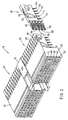
- Figure 1 is a perspective illustration of a fully assembled socket side connector
- Figure 2 is an exploded view, similar to Figure 1, with one wafer not installed;
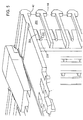
- Figure 3 is a perspective view of a wafer with five tuning fork contacts molded into the wafer body
- Figure 4 is a cross-section through the module with a wafer shown in a fully installed position and two pin contacts having different lengths;
- Figure 5 is a rear perspective view, in cross-section, of the module showing the coring wall wedge shaped protrusion
- Figure 6 is a top plan view of a single wafer showing the offset of the tuning fork beam
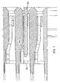
- Figure 7 is a schematic representation of a sectional view through a wafer installed in the module illustrating how the combination of the offset and the contact beams and the wedge shaped protrusion in the coring wall provide a means to prevent the pin contact from stubbing into the base of the throat of the socket contact;
- Figure 8 is a schematic cross-sectional view through a module, wafer and pin contact illustrating the relationship between the surfaces of the socket contact base area, the wedge shape protrusion of the coring wall and the tip of the mating pin contact.
- the socket side connector assembly 10 includes two socket connector housing assemblies 20, each including an insulator module 22, which are connected together by a connector 25. Each of the insulator modules 22 receives a plurality of wafers 30 which are fixed in place in the insulator modules 22, as described below.
- the socket connectors depicted in Figure 1 are from the Winchester Electronics 2 mm product line, but the principles of the present invention are applicable to any two-piece pin and socket connector system employing a tuning fork style socket contact.
- each insulator module 22 accepts eleven wafers 30.
- Each wafer in turn includes five tuning fork style contacts and five right angle pin contacts and therefore each assembly 20 forms an 11 x 5 matrix which includes 55 signal contacts. It is to be understood that any number of signal contacts could be used in the present invention. Additionally, any number of modules 22 can be used. Further, the present invention is illustrated as a right angle connector but the principles of the present invention can be used with any type of tuning fork contact.
- connector assembly 10 is depicted and described as comprising multiple wafers 30 inserted into insulator module 22, it is to be understood that multiple wafers can be replaced by a single larger wafer, i.e., a wafer block, having the appropriate number of tuning fork style contacts and pin contacts.
- each wafer assembly 30 is inserted into the insulator module 22.
- the insulator module 22 has a plurality of contact windows 42, 44, 46, 48, 50 in which a corresponding pin is inserted to be received in a corresponding fork style socket contact 52, 54, 56, 58, 60.
- each of the wafers has a flexible beam type retention mechanism 62 which has a retention member 66 which snaps into a corresponding hole 64 in the insulator module 22.
- Each wafer 30 has an insulated body portion 70.
- Each fork style socket contact has a straight portion 100, an offset portion 102, and a mating portion 104.
- the mating portion 104 includes opposed mating v-ramps 106 each having a front ramp 108 to facilitate insertion of the pin into the tuning fork style contact 52, for example.
- Each tuning fork style contact has a throat defined by the opposing beams 120 and 130 as depicted in Figure 3. Beams 120 and 130 are joined at abase of the throat section 140.
- Each of the tuning fork style contacts 52-60 is electrically connected through housing 70 to a corresponding pin connector 72-80 in a conventional manner.
- pin contacts 152, 154 are shown in the mated position. It should be noted that the pin contacts 152, 154 pass beyond the base of the throat 140 of the socket contacts. As depicted in Figure 4, the two pin contacts 152, 154 have different lengths. Pin contact 154 extends into a receiving portion 254 formed in the wafer 30 and which is positioned and aligned with openings 42-50 for example. As depicted in Figure 4, pin 154 is a sufficient length to be received by receiving portion 254, whereas pin 152 is shorter and is not received by receiving portion 252.
- the configuration of the coring wall 200 which receives the tuning fork style contact is depicted in Figure 5.
- the coring wall 200 includes a central wedge shape portion 202 and an offset wall 204 and a straight wall 206.
- the wedge shape protrusion 202 extends nearly to the base of the contact throat 140 when the wafer 30 is installed in the module 30 such that the pins 152, 154 when inserted through the tuning fork style contact are prevented from stubbing into the base of the throat 140 of the socket contact 52,54.
- Figure 6 is a top view of the wafer 30 depicting the offset of the tuning fork beams 120, 130.
- wedge shaped protrusion 202 of wall 204 conforms to the offset portion 102 of the tuning beams 120, 130 such that the wedge shaped protrusion 202 fits closely or nearly to the base of the throat 140 so that the pins 152, 154 when inserted as depicted in Figure 6, even if the pins 152, 154 bend slightly towards the base of the contact throat 140, are prevented from entering the contact throat and thereby becoming deformed.
- Figure 7 is a view through a section of the wafer 30 installed in the insulator module 22 that depicts how the combination of the offset and the contact beams 120, 130 and the wedge shaped protrusion 202 and the coring wall 200 provide a mechanism to prevent the pin contact 152 from stubbing into the base of the throat 140 of the socket contact 52.
- Figure 8 is another section through the insulator module 22, wafer 30 and pin contact 52 depicting the relationship between the surfaces of the socket contact base area 140, the wedge shaped protrusion 202 of the coring wall 200 and the tip of the mating pin contact 152. These relationships contribute to prevent the pin contact from stubbing into the base of the throat 140 of the socket contact 52.
Landscapes
- Details Of Connecting Devices For Male And Female Coupling (AREA)
- Connector Housings Or Holding Contact Members (AREA)
- Coupling Device And Connection With Printed Circuit (AREA)
Abstract
Description
Claims (18)
- A socket connector for a pin connector, comprising:a module body including a plurality of slots;a plurality of wafers each installable in a corresponding one of said plurality of slots, each wafer having multiple offset tuning forks;said module body having a coring wall having multiple wedge shaped protrusions for each of said offset tuning forks.
- The socket connector of claim 1, wherein said wafer includes a multiple pin receiving portion for receiving a distal end of a corresponding pin.
- The socket connector of claim 1, wherein said module body includes an opening corresponding to each slot and said wafer includes a retention member fitted to said opening of said module body.
- The socket connector of claim 3, wherein said retention member is a flexible beam retention mechanism.
- The socket connector of claim 1, wherein said offset tuning forks comprise two beams joined at a base of a throat section of said tuning forks.
- The socket connector of claim 5, wherein said wedge shaped protrusion extends nearly to the base of said offset tuning forks.
- The socket connector of claim 5, wherein said beams have opposed mating v-ramp ends.
- The socket connector of claim 6, wherein said wafer includes a multiple pin receiving portion for receiving a distal end of a corresponding pin.
- The socket connector of claim 8, wherein said distal end is extendable beyond said base of said offset tuning forks.
- A socket connector for a pin connector, comprising:a module body including a plurality of slots, wherein said module body has a coring wall having multiple wedge shaped protrusions;a wafer block installable in multiple corresponding plurality of slots, each wafer block having multiple offset tuning forks, wherein said tuning forks interact with said protrusions.
- The socket connector of claim 10, wherein said wafer block includes a multiple pin receiving portion for receiving a distal end of a corresponding pin.
- The socket connector of claim 10, wherein said module body includes an opening corresponding to each slot and said wafer includes a retention member fitted to said opening of said module body.
- The socket connector of claim 12, wherein said retention member is a flexible beam retention mechanism.
- The socket connector of claim 10, wherein said offset tuning forks comprise two beams joined at a base of a throat section of said tuning forks.
- The socket connector of claim 14, wherein said wedge shaped protrusion extends nearly to the base of said offset tuning forks.
- The socket connector of claim 14, wherein said beams have opposed mating v-ramp ends.
- The socket connector of claim 15, wherein said wafer includes a multiple pin receiving portion for receiving a distal end of a corresponding pin.
- The socket connector of claim 17, wherein said distal end is extendable beyond said base of said offset tuning forks.
Applications Claiming Priority (4)
| Application Number | Priority Date | Filing Date | Title |
|---|---|---|---|
| US28182601P | 2001-04-06 | 2001-04-06 | |
| US281826P | 2001-04-06 | ||
| US10/114,471 US6709298B2 (en) | 2001-04-06 | 2002-04-03 | Insulator coring and contact configuration to prevent pin stubbing in the throat of tuning fork socket connector contacts |
| US114471 | 2002-04-03 |
Publications (3)
| Publication Number | Publication Date |
|---|---|
| EP1248325A2 true EP1248325A2 (en) | 2002-10-09 |
| EP1248325A3 EP1248325A3 (en) | 2003-12-10 |
| EP1248325B1 EP1248325B1 (en) | 2006-10-04 |
Family
ID=26812227
Family Applications (1)
| Application Number | Title | Priority Date | Filing Date |
|---|---|---|---|
| EP02007766A Expired - Lifetime EP1248325B1 (en) | 2001-04-06 | 2002-04-05 | Insulator coring and contact configuration to prevent pin stubbing in the throat of tuning fork socket connector contacts |
Country Status (4)
| Country | Link |
|---|---|
| US (1) | US6709298B2 (en) |
| EP (1) | EP1248325B1 (en) |
| CN (1) | CN1380724A (en) |
| DE (1) | DE60215070T2 (en) |
Families Citing this family (21)
| Publication number | Priority date | Publication date | Assignee | Title |
|---|---|---|---|---|
| DE10310502A1 (en) * | 2003-03-11 | 2004-09-23 | Molex Inc., Lisle | Earthed electrical connector for GHz signal frequency range, has earthing terminal provided with at least 2 mechanically coupled electrical contacts |
| US7083432B2 (en) * | 2003-08-06 | 2006-08-01 | Fci Americas Technology, Inc. | Retention member for connector system |
| CN100511867C (en) * | 2003-08-06 | 2009-07-08 | Fci公司 | Retainer for connector system |
| US6884117B2 (en) * | 2003-08-29 | 2005-04-26 | Hon Hai Precision Ind. Co., Ltd. | Electrical connector having circuit board modules positioned between metal stiffener and a housing |
| US7074086B2 (en) * | 2003-09-03 | 2006-07-11 | Amphenol Corporation | High speed, high density electrical connector |
| US6875031B1 (en) * | 2003-12-05 | 2005-04-05 | Hon Hai Precision Ind. Co., Ltd. | Electrical connector with circuit board module |
| US6932649B1 (en) * | 2004-03-19 | 2005-08-23 | Tyco Electronics Corporation | Active wafer for improved gigabit signal recovery, in a serial point-to-point architecture |
| US7662422B2 (en) * | 2005-04-05 | 2010-02-16 | Furtaw Louis F | Crisp meat-based food snacks |
| US7396259B2 (en) * | 2005-06-29 | 2008-07-08 | Fci Americas Technology, Inc. | Electrical connector housing alignment feature |
| US7175479B1 (en) * | 2006-04-25 | 2007-02-13 | Tyco Electronics Corporation | Modular connector assembly with stamped retention latch members |
| CN101496231B (en) * | 2006-05-23 | 2012-05-30 | Fci公司 | Electrical connectors, connector substrates and connectors, and tools for assembling connectors |
| DE202006016424U1 (en) * | 2006-10-20 | 2007-01-04 | Phoenix Contact Gmbh & Co. Kg | Electric contact device with an insulating housing with fastening recesses in which the contacts engage |
| DE102007027430A1 (en) * | 2007-06-14 | 2008-12-24 | Tyco Electronics Amp Gmbh | Holder of two plugs |
| US7789676B2 (en) * | 2008-08-19 | 2010-09-07 | Tyco Electronics Corporation | Electrical connector with electrically shielded terminals |
| JP4847598B2 (en) * | 2010-06-10 | 2011-12-28 | ファナック株式会社 | connector |
| WO2013022889A2 (en) | 2011-08-08 | 2013-02-14 | Molex Incorporated | Connector with tuned channel |
| CN103187651B (en) * | 2011-12-27 | 2015-01-14 | 凡甲电子(苏州)有限公司 | Electric connector |
| US9099820B2 (en) * | 2013-09-18 | 2015-08-04 | Delphi Technologies, Inc. | Electronics module with a side entry connection |
| US9118147B1 (en) * | 2014-02-19 | 2015-08-25 | Tyco Electronics Corporation | Electrical connector |
| US9837753B1 (en) * | 2016-12-21 | 2017-12-05 | Six Sights Corporation | Module outlet |
| US11424573B2 (en) | 2020-09-24 | 2022-08-23 | Apple Inc. | Magnetic connectors with self-centering floating contacts |
Family Cites Families (13)
| Publication number | Priority date | Publication date | Assignee | Title |
|---|---|---|---|---|
| GB8431759D0 (en) | 1984-12-17 | 1985-01-30 | Amp Great Britain | Electrical connector & terminal |
| DE69018000T2 (en) * | 1989-10-10 | 1995-09-28 | Whitaker Corp | Backplane connector with matched impedance. |
| JP2700117B2 (en) * | 1992-07-28 | 1998-01-19 | 矢崎総業株式会社 | Connector terminal insertion structure |
| US5472358A (en) | 1994-04-01 | 1995-12-05 | Genrife Company Limited | Contact of single pitch arrangement in strip stock |
| JP3132706B2 (en) * | 1994-06-06 | 2001-02-05 | 矢崎総業株式会社 | Female terminal for connector |
| DE69525138T2 (en) | 1994-12-15 | 2002-08-22 | Whitaker Corp | First pole contacts last, earth contact interrupting connector |
| US5664969A (en) * | 1995-08-24 | 1997-09-09 | Molex Incorporated | Electrical connector with improved terminal positioning means |
| US5795191A (en) | 1996-09-11 | 1998-08-18 | Preputnick; George | Connector assembly with shielded modules and method of making same |
| JP3379882B2 (en) | 1997-02-18 | 2003-02-24 | 本多通信工業株式会社 | Connector and its surface mounting method |
| DE69728548T2 (en) | 1997-12-17 | 2005-02-24 | Fci | Connector with floating terminals, and terminal for such a connector |
| DE19825971C1 (en) * | 1998-06-10 | 1999-11-11 | Harting Kgaa | Multipin electrical plug connector, e.g. for printed circuit board |
| JP4068286B2 (en) | 2000-06-30 | 2008-03-26 | 株式会社東芝 | Manufacturing method of semiconductor device |
| US6347962B1 (en) * | 2001-01-30 | 2002-02-19 | Tyco Electronics Corporation | Connector assembly with multi-contact ground shields |
-
2002
- 2002-04-03 US US10/114,471 patent/US6709298B2/en not_active Expired - Fee Related
- 2002-04-05 DE DE60215070T patent/DE60215070T2/en not_active Withdrawn - After Issue
- 2002-04-05 EP EP02007766A patent/EP1248325B1/en not_active Expired - Lifetime
- 2002-04-08 CN CN02106169.6A patent/CN1380724A/en active Pending
Also Published As
| Publication number | Publication date |
|---|---|
| DE60215070D1 (en) | 2006-11-16 |
| CN1380724A (en) | 2002-11-20 |
| US20020146941A1 (en) | 2002-10-10 |
| EP1248325B1 (en) | 2006-10-04 |
| DE60215070T2 (en) | 2007-05-10 |
| US6709298B2 (en) | 2004-03-23 |
| EP1248325A3 (en) | 2003-12-10 |
Similar Documents
| Publication | Publication Date | Title |
|---|---|---|
| US6709298B2 (en) | Insulator coring and contact configuration to prevent pin stubbing in the throat of tuning fork socket connector contacts | |
| US6695627B2 (en) | Profiled header ground pin | |
| CN113517619B (en) | Receptacle connector with contact assembly | |
| EP0569893B1 (en) | Low profile electrical connector | |
| US20100041266A1 (en) | Power connector with integrated signal connector | |
| US7402087B2 (en) | Electric connector | |
| JP3301329B2 (en) | connector | |
| EP0780933A2 (en) | Electrical connector for circuit board | |
| US6884106B2 (en) | Electrical connector assembly | |
| US20050118891A1 (en) | Female terminal for heavy current and female terminal for heavy current with shell | |
| US7114998B2 (en) | Divided connector and connector assembly | |
| CN1172365A (en) | Board-to-Board Connector Assemblies | |
| US6086419A (en) | Electrical connector assembly | |
| US20050287860A1 (en) | Interlocking member for an electrical connector | |
| EP2328242A1 (en) | Electrical connector | |
| US7094073B2 (en) | Relay connection circuit and relay connector | |
| US6227898B1 (en) | Card edge connector with removable rail guide | |
| CN109980404B (en) | Socket connector housing with hold-down ribs | |
| EP0944133A1 (en) | Electrical connector for flat flexible circuits | |
| KR100366951B1 (en) | Receptacle Contact and Connector Using Same | |
| US6390842B1 (en) | Card edge connector with deflective latch members | |
| US4726792A (en) | Electrical connector having electrical contacts provided with retention means | |
| JP6172760B2 (en) | Connector housing | |
| US6679734B2 (en) | Subminiature electrical connector multi-pin grounding/discrete circuit bussing module and integral connector backshell | |
| US6485312B1 (en) | Electrical connector assembly |
Legal Events
| Date | Code | Title | Description |
|---|---|---|---|
| PUAI | Public reference made under article 153(3) epc to a published international application that has entered the european phase |
Free format text: ORIGINAL CODE: 0009012 |
|
| AK | Designated contracting states |
Kind code of ref document: A2 Designated state(s): AT BE CH CY DE DK ES FI FR GB GR IE IT LI LU MC NL PT SE TR |
|
| AX | Request for extension of the european patent |
Free format text: AL;LT;LV;MK;RO;SI |
|
| PUAL | Search report despatched |
Free format text: ORIGINAL CODE: 0009013 |
|
| AK | Designated contracting states |
Kind code of ref document: A3 Designated state(s): AT BE CH CY DE DK ES FI FR GB GR IE IT LI LU MC NL PT SE TR |
|
| AX | Request for extension of the european patent |
Extension state: AL LT LV MK RO SI |
|
| RAP1 | Party data changed (applicant data changed or rights of an application transferred) |
Owner name: LITTON SYSTEMS, INC. |
|
| 17P | Request for examination filed |
Effective date: 20040609 |
|
| AKX | Designation fees paid |
Designated state(s): DE FR GB |
|
| 17Q | First examination report despatched |
Effective date: 20040916 |
|
| GRAP | Despatch of communication of intention to grant a patent |
Free format text: ORIGINAL CODE: EPIDOSNIGR1 |
|
| GRAS | Grant fee paid |
Free format text: ORIGINAL CODE: EPIDOSNIGR3 |
|
| GRAA | (expected) grant |
Free format text: ORIGINAL CODE: 0009210 |
|
| AK | Designated contracting states |
Kind code of ref document: B1 Designated state(s): DE FR GB |
|
| REG | Reference to a national code |
Ref country code: GB Ref legal event code: FG4D |
|
| REF | Corresponds to: |
Ref document number: 60215070 Country of ref document: DE Date of ref document: 20061116 Kind code of ref document: P |
|
| ET | Fr: translation filed | ||
| PLBI | Opposition filed |
Free format text: ORIGINAL CODE: 0009260 |
|
| 26 | Opposition filed |
Opponent name: ERNI ELECTRONICS GMBH Effective date: 20070704 |
|
| PLAX | Notice of opposition and request to file observation + time limit sent |
Free format text: ORIGINAL CODE: EPIDOSNOBS2 |
|
| PG25 | Lapsed in a contracting state [announced via postgrant information from national office to epo] |
Ref country code: DE Free format text: LAPSE BECAUSE OF THE APPLICANT RENOUNCES Effective date: 20070917 |
|
| REG | Reference to a national code |
Ref country code: FR Ref legal event code: RT |
|
| GBPC | Gb: european patent ceased through non-payment of renewal fee |
Effective date: 20070405 |
|
| PLBB | Reply of patent proprietor to notice(s) of opposition received |
Free format text: ORIGINAL CODE: EPIDOSNOBS3 |
|
| PG25 | Lapsed in a contracting state [announced via postgrant information from national office to epo] |
Ref country code: GB Free format text: LAPSE BECAUSE OF NON-PAYMENT OF DUE FEES Effective date: 20070405 |
|
| REG | Reference to a national code |
Ref country code: GB Ref legal event code: S29 |
|
| PG25 | Lapsed in a contracting state [announced via postgrant information from national office to epo] |
Ref country code: FR Free format text: LAPSE BECAUSE OF NON-PAYMENT OF DUE FEES Effective date: 20070430 |
|
| REG | Reference to a national code |
Ref country code: GB Ref legal event code: S29 |
|
| PLBD | Termination of opposition procedure: decision despatched |
Free format text: ORIGINAL CODE: EPIDOSNOPC1 |
|
| PLBM | Termination of opposition procedure: date of legal effect published |
Free format text: ORIGINAL CODE: 0009276 |
|
| STAA | Information on the status of an ep patent application or granted ep patent |
Free format text: STATUS: OPPOSITION PROCEDURE CLOSED |
|
| 27C | Opposition proceedings terminated |
Effective date: 20090516 |