EP1246306A2 - Electrical connector - Google Patents
Electrical connector Download PDFInfo
- Publication number
- EP1246306A2 EP1246306A2 EP02290775A EP02290775A EP1246306A2 EP 1246306 A2 EP1246306 A2 EP 1246306A2 EP 02290775 A EP02290775 A EP 02290775A EP 02290775 A EP02290775 A EP 02290775A EP 1246306 A2 EP1246306 A2 EP 1246306A2
- Authority
- EP
- European Patent Office
- Prior art keywords
- connector
- capacitive coupling
- conductor
- board
- coupling plate
- Prior art date
- Legal status (The legal status is an assumption and is not a legal conclusion. Google has not performed a legal analysis and makes no representation as to the accuracy of the status listed.)
- Granted
Links
Images


Classifications
-
- H—ELECTRICITY
- H01—ELECTRIC ELEMENTS
- H01R—ELECTRICALLY-CONDUCTIVE CONNECTIONS; STRUCTURAL ASSOCIATIONS OF A PLURALITY OF MUTUALLY-INSULATED ELECTRICAL CONNECTING ELEMENTS; COUPLING DEVICES; CURRENT COLLECTORS
- H01R13/00—Details of coupling devices of the kinds covered by groups H01R12/70 or H01R24/00 - H01R33/00
- H01R13/648—Protective earth or shield arrangements on coupling devices, e.g. anti-static shielding
-
- H—ELECTRICITY
- H01—ELECTRIC ELEMENTS
- H01R—ELECTRICALLY-CONDUCTIVE CONNECTIONS; STRUCTURAL ASSOCIATIONS OF A PLURALITY OF MUTUALLY-INSULATED ELECTRICAL CONNECTING ELEMENTS; COUPLING DEVICES; CURRENT COLLECTORS
- H01R13/00—Details of coupling devices of the kinds covered by groups H01R12/70 or H01R24/00 - H01R33/00
- H01R13/66—Structural association with built-in electrical component
- H01R13/719—Structural association with built-in electrical component specially adapted for high frequency, e.g. with filters
-
- H—ELECTRICITY
- H01—ELECTRIC ELEMENTS
- H01R—ELECTRICALLY-CONDUCTIVE CONNECTIONS; STRUCTURAL ASSOCIATIONS OF A PLURALITY OF MUTUALLY-INSULATED ELECTRICAL CONNECTING ELEMENTS; COUPLING DEVICES; CURRENT COLLECTORS
- H01R12/00—Structural associations of a plurality of mutually-insulated electrical connecting elements, specially adapted for printed circuits, e.g. printed circuit boards [PCB], flat or ribbon cables, or like generally planar structures, e.g. terminal strips, terminal blocks; Coupling devices specially adapted for printed circuits, flat or ribbon cables, or like generally planar structures; Terminals specially adapted for contact with, or insertion into, printed circuits, flat or ribbon cables, or like generally planar structures
- H01R12/50—Fixed connections
- H01R12/51—Fixed connections for rigid printed circuits or like structures
- H01R12/52—Fixed connections for rigid printed circuits or like structures connecting to other rigid printed circuits or like structures
-
- H—ELECTRICITY
- H01—ELECTRIC ELEMENTS
- H01R—ELECTRICALLY-CONDUCTIVE CONNECTIONS; STRUCTURAL ASSOCIATIONS OF A PLURALITY OF MUTUALLY-INSULATED ELECTRICAL CONNECTING ELEMENTS; COUPLING DEVICES; CURRENT COLLECTORS
- H01R12/00—Structural associations of a plurality of mutually-insulated electrical connecting elements, specially adapted for printed circuits, e.g. printed circuit boards [PCB], flat or ribbon cables, or like generally planar structures, e.g. terminal strips, terminal blocks; Coupling devices specially adapted for printed circuits, flat or ribbon cables, or like generally planar structures; Terminals specially adapted for contact with, or insertion into, printed circuits, flat or ribbon cables, or like generally planar structures
- H01R12/70—Coupling devices
- H01R12/71—Coupling devices for rigid printing circuits or like structures
- H01R12/712—Coupling devices for rigid printing circuits or like structures co-operating with the surface of the printed circuit or with a coupling device exclusively provided on the surface of the printed circuit
- H01R12/716—Coupling device provided on the PCB
-
- H—ELECTRICITY
- H01—ELECTRIC ELEMENTS
- H01R—ELECTRICALLY-CONDUCTIVE CONNECTIONS; STRUCTURAL ASSOCIATIONS OF A PLURALITY OF MUTUALLY-INSULATED ELECTRICAL CONNECTING ELEMENTS; COUPLING DEVICES; CURRENT COLLECTORS
- H01R13/00—Details of coupling devices of the kinds covered by groups H01R12/70 or H01R24/00 - H01R33/00
- H01R13/66—Structural association with built-in electrical component
- H01R13/719—Structural association with built-in electrical component specially adapted for high frequency, e.g. with filters
- H01R13/7195—Structural association with built-in electrical component specially adapted for high frequency, e.g. with filters with planar filters with openings for contacts
Definitions
- the present invention relates to an electrical connector for interconnecting two boards or equivalent.
- the board-to-board electrical connector has a pair of male and female connectors each having one or more contacts.
- the pair of male and female connectors When the pair of male and female connectors are fitted to each other, their contacts are brought into physical contact with each other and thereby the two boards or equivalent are electrically connected.
- the contacts of the pair of male and female connectors of the board-to-board electrical connector are brought into physical contact with each other, for the reason of which this type of board-to-board electrical connector does not have the band-pass characteristic that only a signal within a specified frequency band transmits from one of the pair of connectors to the other.
- a noise-cut filter is additionally required for cutting noise transmitted from one connector to the other. Also, for allowing only a signal within a specified frequency band to transmit from the one connector to the other, an additional band-pass filter having the corresponding band-pass characteristic is required.
- a board-to-board electrical connector of the present invention comprises a first connector having a first conductor; and a second connector having a second conductor which is brought into the state in which at least a part thereof confronts a part of the first conductor with spaced therefrom, when the second connector is fitted to the first connector, wherein capacitance between the first conductor and the second conductor is adjusted so that only a signal within a specified frequency band can be allowed to pass from the first conductor to the second conductor.
- the board-to-board electrical connector thus constructed, when the first connecter and the second connector are fitted to each other, the first conductor and the second conductor are brought into the state in which they partly confront each other, with spaced from each other, and also the capacitance between the first conductor and the second conductor is adjusted so that only a signal within a specified frequency band can be allowed to pass from the first conductor to the second conductor, whereby the board-to-board electrical connector having the specified band-pass characteristic is achieved.
- the first connector and the second connector are fitted to each other, the first and second conductors are brought into non-contact with each other, whereby increase in impedance, which is caused by the conductors being contacted with each other as in the conventional contact type, is prevented. As a result of this, deterioration of the band-pass characteristic of the board-to-board electrical connector is prevented.
- the capacitance between the first conductor and the second conductor is adjusted by adjusting permittivity between the first conductor and the second conductor, a distance between confronting portions of the first and second conductors, or an area formed by the confronting portions of the first and second conductors.
- the capacitance between the first conductor and the second conductor can be easily adjusted to a specified value, and as such can provide the board-to-board electrical connector having a specified band-pass characteristic with ease.
- a plurality of conductor plates provided in at least either of the first connector and the second connector confront each other;
- the first connector is provided with one or more first conductors which are located between the plurality of conductor plates of each pair when the first connector and the second connector are fitted to each other;
- the second connector is provided with one or more second conductors which are located between the plurality of conductor plates of each pair and also are brought into capacitive coupling with the first conductor when the first connector and the second connector are fitted to each other.
- the board-to-board electrical connector thus constructed, since the conductor plates are located between the plurality of signal lines of each pair which are formed by the first conductors and the second conductors corresponding thereto, the signals transmitting through the respective signal lines can be prevented from interfering with each other. In addition, when the capacitances between the first conductors and the second conductors corresponding thereto of each pair are adjusted to values different from each other, the board-to-board electrical connector having different band-pass characteristics can be achieved.
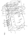
- a board-to-board electrical connector 1 comprising a pair of male and female connectors shown in FIGS. 1-3 includes a connector 2 and a connector 3.
- the connector 2 comprises a housing 21, a group of terminals 22 mainly used for slow signals held in the housing 21, and a group of terminals 23 mainly used for fast signals held in the housing 21, as shown in FIG. 2.
- the housing 21 is formed in one piece which comprises a terminal-group holding portion 21a for holding the group of terminals 22 and a terminal-group holding portion 21b for holding the group of terminals 23.
- the terminal-group holding portion 21a has a concave portion 21c.
- the terminal-group holding portion 21b has three concave portions 21d, 21e and 21f.
- the group of terminals 22 comprises a total of eight contacts 22a, 22b, 22c, 22d, 22e, 22f, 22g and 22h which are identical in shape and are aligned in two columns and four rows. These contacts are accommodated in the concave portion 21c of the terminal-group holding portion 21a of the housing 21.
- the group of terminals 23 is held in the terminal-group holding portion 21b of the housing 21 and comprises two capacitive coupling plates 24 and 25 and three conductor plates 26, 27 and 28.
- the capacitive coupling plate 24 which is a conductor having a flat-plate form, is held in the housing 21 so as to be accommodated in the concave portion 21d of the terminal-group holding portion 21b.
- the capacitive coupling plate 24 comes into the state in which it partly confronts a part of a capacitive coupling plate 34 of the connector 3 mentioned later, with spaced therefrom.
- the capacitive coupling plate 25 which is a conductor having a flat-plate form, is held in the housing 21 so as to be accommodated in the concave portion 21e of the terminal-group holding portion 21b and so as to be parallel with the capacitive coupling plate 24.
- the capacitive coupling plate 25 comes into the state in which it partly confronts a part of a capacitive coupling plate 35 of the connector 3 mentioned later, with spaced therefrom.
- the capacitive coupling plate 24 forms a signal line S1 for being transmitted signals from a printed circuit board (not shown) mounting the connector 2 thereon to a printed circuit board (not shown) mounting the connector 3 thereon or vice versa.
- the capacitive coupling plate 25 forms a signal line S2 for being transmitting signals from the printed circuit board (not shown) mounting the connector 2 thereon to the printed circuit board (not shown) mounting the connector 3 thereon or vice versa.
- Each of the conductor plates 26, 27 and 28 has a flat-plate form.
- the conductor plate 26 is held in the housing 21 so as to be accommodated in the concave portion 21d of the terminal-group holding portion 21b and so as to be parallel with the capacitive coupling plate 24.
- the conductor plate 27 is held in the housing 21 so as to be accommodated in the concave portion 21e of the terminal-group holding portion 21b and so as to be parallel with the capacitive coupling plate 25.
- the conductor plate 28 is held in the housing 21 so as to be accommodated in the concave portion 21f of the terminal-group holding portion 21c and so as to be parallel with the conductor plates 26 and 27.
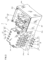
- the connector 3 comprises a housing 31, a group of terminals 32 mainly used for slow signals held in the housing 31, and a group of terminals 33 mainly used for fast signals held in the housing 31, as shown in FIG. 3.
- the housing 31 is formed in one piece which comprises a terminal-group holding portion 31a for holding the group of terminals 32 and a terminal-group holding portion 31b for holding the group of terminals 33.
- the terminal-group holding portion 31a has a convex portion 31c.
- the terminal-group holding portion 31b has a "U-shaped" frame portion 31d and includes projecting portions 31e and 31f.
- the group of terminals 32 comprises a total of eight contacts 32a, 32b, 32c, 32d, 32e, 32f, 32g and 32h which are identical in shape and are aligned in two columns and four rows. These contacts are held in side walls of the convex portion 31c of the terminal-group holding portion 31a of the housing 31.
- the group of terminals 33 is held in the terminal-group holding portion 31b of the housing 31 and comprises two capacitive coupling plates 34 and 35.
- the capacitive coupling plate 34 is a conductor having a flat-plate form.
- the capacitive coupling plate 34 is held in the housing 31 so as to be located between the projecting portions 31e and 31f provided in the terminal-group holding portion 31b.
- the capacitive coupling plate 34 is held in the housing 31 so that when the connector 2 and the connector 3 are fitted to each other, it can be parallel with the conductor plate 26 of the connector 2 and also can confront a part of the capacitive coupling plate 24, with spaced therefrom.
- the capacitive coupling plate 35 is a conductor having a flat-plate form.
- the capacitive coupling plate 35 is held in the housing 31 so as to be located at the opposite side to the projecting portion 31e with respect to the projecting portion 31f provided in the terminal-group holding portion 31b.
- the capacitive coupling plate 35 is held in the housing 31 so that when the connector 2 and the connector 3 are fitted to each other, it can be parallel with the conductor plate 27 of the connector 2 and also can confront a part of the capacitive coupling plate 25, with spaced therefrom.
- the terminal-group holding portion 21b of the connector 2 is accommodated in the frame portion 31d of the terminal-group holding portion 31b of the connector 3. Then, the projecting portion 31e provided in the housing 31 of the connector 3 and the capacitive coupling plate 34 of the connector are accommodated in the concave portion 21d provided in the terminal-group holding portion 21b of the connector 2 so as to be located between the conductor plate 26 and capacitive coupling plate 24 of the connector 2. Then, the capacitive coupling plate 24 and the capacitive coupling plate 34 partly confront each other in the non-contact state.
- the projecting portion 31f provided in the housing 31 of the connector 3 and the capacitive coupling plate 35 of the connector 3 are accommodated in the concave portion 21e provided in the terminal-group holding portion 21b of the connector 2 so as to be located between the conductor plate 27 and capacitive coupling plate 25 of the connector 2. Then, the capacitive coupling plate 25 and the capacitive coupling plate 35 partly confront each other in the non-contact state.
- an inductor 51 corresponds to the inductance of the capacitive coupling plate 24, and the inductance of the inductor 51 is represented here as L1.
- An inductor 52 corresponds to the inductance of the capacitive coupling plate 34, and the inductance of the inductor 52 is represented here as L2.
- a capacitor 53 corresponds to the capacitance between the capacitive coupling plate 24 and the capacitive coupling plate 34, and the capacitance of the capacitor 53 is represented here as C1.
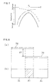
- the inductors 51 and 52 have a frequency characteristic that attenuation increases with increase in frequency f, as schematically shown in FIG. 5.
- the capacitor 53 has a frequency characteristic that attenuation decreases with increase in frequency f, as schematically shown in FIG. 6. Therefore, an outline of attenuation of the equivalent circuit shown in FIG. 4 is given by the sum of the attenuation by the capacitor 53 and the attenuation by the inductors 51 and 52, as is represented in full line in FIG. 7. Therefore, the equivalent circuit relating to the capacitive coupling plates 24 and 34 has a band-pass characteristic. It is to be noted that a dotted line in FIG. 7 represents the sum of the attenuation by the inductor 51 and the attenuation by the inductor 52 and a dashed line in FIG. 7 represents the attenuation by the capacitor 53.
- the value of the frequency fc varies depending on values of the inductances L1 and L2 and a value of the capacitance C1.
- the value of the frequency fc at which the attenuation becomes minimum is varied depending on the values of the inductances L1 and L2 and the value of the capacitance C1.
- the absolute value of the impedance Z varies depending on the values of the inductances L1 and L2 and the value of the capacitance C1.
- the attenuation of the equivalent circuit varies depending on the values of the inductances L1 and L2 and the value of the capacitance C1. Therefore, the bandwidth for the signals to pass varies depending on the values of the inductances L1 and L2 and the value of the capacitance C1.
- the band-pass characteristic of the equivalent circuit can vary by being varied the values of the inductances L1 and L2 and the value of the capacitance C1.
- an equivalent circuit relating to the capacitive coupling plate 25 and the capacitive coupling plate 35 has a band-pass characteristic that is determined by the value of the capacitance and the value of the inductance. As a result of this, only a signal within a specified frequency band can be allowed to pass from the capacitive coupling plate 25 to the capacitive coupling plate 35 or vice versa.
- a capacitance C between two flat-plate electrodes is expressed by the following equation (5)
- C ⁇ S d
- S an area of the flat-plate electrodes
- d a distance between the flat-plate electrodes
- ⁇ the permittivity therebetween.
- the value of the capacitance C1 can be adjusted by properly adjusting the values of the area A1 and the between-opposing-plates distance d1.
- the band-pass characteristic of the equivalent circuit relating to the capacitive coupling plate 24 and the capacitive coupling plate 34 is determined by the value of the capacitance C1 of the capacitor 53 and the values of the inductances L1 and L2 of the inductors 51 and 52, as mentioned above, if the value of the capacitance C1 of the capacitor 53 is set at a specified value by adjusting the values of the area A1 and the between-opposing-plates distance d1, the equivalent circuit can have a specified band-pass characteristic.
- the band-pass characteristic of the equivalent circuit relating to the capacitive coupling plate 25 and the capacitive coupling plate 35 can have a specified band-pass characteristic by setting the value of the capacitance at a specified value by adjusting an area formed by confronting portions of the capacitive coupling plates 25 and 35 and a distance between the confronting portions thereof.
- Modification may be made in the present invention such that dielectrics are disposed between the capacitive coupling plate 24 and the capacitive coupling plate 34 and between the capacitive coupling plate 25 and the capacitive coupling plate 35, respectively, so that the value of the capacitance can be adjusted by changing the kinds of dielectrics or the permittivity. Also, the value of the capacitance may be adjusted by any selective combination among the kinds of dielectrics (the permittivity), the area formed by confronting portions of the capacitive coupling plates, and the distance between the confronting portions thereof.
- the board-to-board electrical connector having the specified band-pass characteristic can be achieved by adjusting the value of the capacitance between the capacitive coupling plates.
- a frequency of signals transmitting from one printed circuit board to the other printed circuit board can fall within a specified frequency band without any additional band-pass filter, and also the noise can be cut without any additional band-pass filter.
- the board-to-board electrical connector having different band-pass characteristics can be achieved by setting the area formed by the confronting portions of the capacitive coupling plates 24 and 34 and the distance between the confronting portions thereof, and the area formed by the confronting portions of the capacitive coupling plates 25 and 35 and the distance between the confronting portions thereof at different values.
- the capacitive coupling plate 24 and the capacitive coupling plate 34 are put in non-contact with each other, variation of the band-pass characteristic caused by deterioration of the capacitive coupling plates 24 and 34 can be prevented.
- the capacitive coupling plate 25 and the capacitive coupling plate 35 are put in non-contact with each other, variation of the band-pass characteristic caused by deterioration of the capacitive coupling plates 25 and 35 can be prevented.
- the conductor plate 27 exists between the signal lines S1 and S2, the signal transmitting through the signal line S1 and the signal transmitting through the signal line S2 can be prevented form interfering with each other.
- the present invention should not be limited to the embodiment illustrated above and various changes and modifications in design may be made in the invention within the scope of the claims.
- the two signal lines are formed, any adequate number of signal lines may selectively be formed.
- the conductor plates 26, 27 and 28 are comprised in the connector 2, they may alternatively be comprised in the connector 3.
- the conductor plates may be comprised in both of the connectors 2 and 3 so that when the connectors 2 and 3 are fitted to each other, the conductor plates comprised in the both connectors respectively can be brought into contact with each other to form a grand plane.
- a plurality of capacitive coupling plates may be used to form a plurality of signal lines between the conductor plates 26 and 27. Further, it is needless to say that the present invention is applicable to various types of electrical connectors as well as to the board-to-board electrical connector.
Landscapes
- Details Of Connecting Devices For Male And Female Coupling (AREA)
- Filters And Equalizers (AREA)
- Coupling Device And Connection With Printed Circuit (AREA)
Abstract
Description
Claims (3)
- An electrical connector (1) comprising:wherein capacitance between the first conductor (24) and the second conductor (34) is adjusted so that only a signal within a specified frequency band can be allowed to pass from the first conductor to the second conductor.a first connector (2) having a first conductor (24); anda second connector (3) having a second conductor (34) which is brought into the state in which at least a part thereof confronts a part of the first conductor, with spaced therefrom, when the second connector is fitted to the first connector,
- The electrical connector according to Claim 1, wherein the capacitance between the first conductor (24) and the second conductor (34) is adjusted by adjusting permittivity between the first conductor and the second conductor, a distance between confronting portions of the first and second conductors, or an area formed by the confronting portions of the first and second conductors.
- The electrical connector according to claims 1 or 2, wherein a plurality of conductor plates (26, 27, 28) provided in at least either of the first connector (2) and the second connector (3) confront each other, wherein the first connector (2) is provided with one or more first conductors (24, 25) which are located between the plurality of conductor plates of each pair when the first connector and the second connector are fitted to each other, and wherein the second connector (3) is provided with one or more second conductors (34, 35) which are located between the plurality of conductor plates of each pair and also are brought into capacitive coupling with the first conductor when the first connector and the second connector are fitted to each other.
Applications Claiming Priority (2)
| Application Number | Priority Date | Filing Date | Title |
|---|---|---|---|
| JP2001092178A JP2002289309A (en) | 2001-03-28 | 2001-03-28 | Electrical connector |
| JP2001092178 | 2001-03-28 |
Publications (3)
| Publication Number | Publication Date |
|---|---|
| EP1246306A2 true EP1246306A2 (en) | 2002-10-02 |
| EP1246306A3 EP1246306A3 (en) | 2004-05-19 |
| EP1246306B1 EP1246306B1 (en) | 2006-04-26 |
Family
ID=18946686
Family Applications (1)
| Application Number | Title | Priority Date | Filing Date |
|---|---|---|---|
| EP02290775A Expired - Lifetime EP1246306B1 (en) | 2001-03-28 | 2002-03-27 | Electrical connector |
Country Status (7)
| Country | Link |
|---|---|
| US (1) | US7064626B2 (en) |
| EP (1) | EP1246306B1 (en) |
| JP (1) | JP2002289309A (en) |
| KR (1) | KR100485999B1 (en) |
| CN (1) | CN1224142C (en) |
| DE (1) | DE60210854T2 (en) |
| TW (1) | TW552747B (en) |
Cited By (1)
| Publication number | Priority date | Publication date | Assignee | Title |
|---|---|---|---|---|
| WO2009151803A1 (en) * | 2008-06-10 | 2009-12-17 | Molex Incorporated | Capacitively coupled connector for flexible printed circuit applications |
Families Citing this family (6)
| Publication number | Priority date | Publication date | Assignee | Title |
|---|---|---|---|---|
| US7617336B1 (en) | 2005-04-05 | 2009-11-10 | Sprint Communications Company L.P. | Blade computing system |
| US7351120B1 (en) * | 2007-02-05 | 2008-04-01 | International Business Machines Corporation | Adjustable impedance electrical connector |
| JP4932789B2 (en) * | 2008-04-28 | 2012-05-16 | モレックス インコーポレイテド | Connector and terminal holder |
| JP5113101B2 (en) * | 2009-01-30 | 2013-01-09 | モレックス インコーポレイテド | Electrical circuit connection structure and electrical circuit connection method |
| JP2010177103A (en) | 2009-01-30 | 2010-08-12 | Molex Inc | Connector and terminal holder |
| KR101331934B1 (en) * | 2012-05-16 | 2013-11-21 | 주식회사 텔콘 | Rf connector |
Family Cites Families (13)
| Publication number | Priority date | Publication date | Assignee | Title |
|---|---|---|---|---|
| JP2663166B2 (en) | 1989-02-23 | 1997-10-15 | デイエツクスアンテナ株式会社 | High frequency rotary joint |
| JPH02235417A (en) | 1989-03-08 | 1990-09-18 | Fujitsu Ltd | Multi-frequency series resonance circuit |
| JPH0334704A (en) * | 1989-06-30 | 1991-02-14 | Harada Ind Co Ltd | Through-glass antenna for automobile radio |
| JPH0341601A (en) | 1989-07-07 | 1991-02-22 | Matsushita Electric Ind Co Ltd | Video floppy recording and playback device |
| US5073761A (en) * | 1990-06-05 | 1991-12-17 | Westinghouse Electric Corp. | Non-contacting radio frequency coupler connector |
| JPH0629047A (en) | 1992-07-10 | 1994-02-04 | Meidensha Corp | Electric connection method for electrolytic cell |
| ATE149748T1 (en) * | 1992-11-03 | 1997-03-15 | Whitaker Corp | BAND FILTER AND METHOD OF ATTACHING TO AN ELECTRICAL CONNECTOR |
| US5432486A (en) * | 1993-05-20 | 1995-07-11 | Northern Telecom Limited | Capacitive and inductive coupling connector |
| JP2513430B2 (en) | 1993-10-18 | 1996-07-03 | 日本電気株式会社 | Dielectric filter |
| PL179922B1 (en) * | 1996-01-02 | 2000-11-30 | Ibm | High-frequency pcmcia junction |
| JP3011671B2 (en) | 1997-02-18 | 2000-02-21 | 株式会社東芝 | Coaxial connector |
| US6106519A (en) * | 1997-06-30 | 2000-08-22 | Ethicon Endo-Surgery, Inc. | Capacitively coupled electrosurgical trocar |
| JPH1186980A (en) | 1997-09-02 | 1999-03-30 | Canon Inc | connector |
-
2001
- 2001-03-28 JP JP2001092178A patent/JP2002289309A/en active Pending
-
2002
- 2002-03-01 TW TW091103831A patent/TW552747B/en not_active IP Right Cessation
- 2002-03-07 US US10/093,147 patent/US7064626B2/en not_active Expired - Fee Related
- 2002-03-16 KR KR10-2002-0014256A patent/KR100485999B1/en not_active Expired - Fee Related
- 2002-03-27 EP EP02290775A patent/EP1246306B1/en not_active Expired - Lifetime
- 2002-03-27 DE DE60210854T patent/DE60210854T2/en not_active Expired - Fee Related
- 2002-03-28 CN CNB021082545A patent/CN1224142C/en not_active Expired - Fee Related
Cited By (2)
| Publication number | Priority date | Publication date | Assignee | Title |
|---|---|---|---|---|
| WO2009151803A1 (en) * | 2008-06-10 | 2009-12-17 | Molex Incorporated | Capacitively coupled connector for flexible printed circuit applications |
| US8475181B2 (en) | 2008-06-10 | 2013-07-02 | Molex Incorporated | Capacitively coupled connector for flexible printed circuit applications |
Also Published As
| Publication number | Publication date |
|---|---|
| US7064626B2 (en) | 2006-06-20 |
| JP2002289309A (en) | 2002-10-04 |
| CN1378312A (en) | 2002-11-06 |
| DE60210854T2 (en) | 2007-05-16 |
| HK1050430A1 (en) | 2003-06-20 |
| DE60210854D1 (en) | 2006-06-01 |
| US20020182937A1 (en) | 2002-12-05 |
| KR20020077060A (en) | 2002-10-11 |
| EP1246306A3 (en) | 2004-05-19 |
| EP1246306B1 (en) | 2006-04-26 |
| CN1224142C (en) | 2005-10-19 |
| KR100485999B1 (en) | 2005-04-29 |
| TW552747B (en) | 2003-09-11 |
Similar Documents
| Publication | Publication Date | Title |
|---|---|---|
| US6979226B2 (en) | Connector | |
| EP1239552B1 (en) | Connector having signal contacts and ground contacts in a specific arrangement | |
| US5004426A (en) | Electrically connecting | |
| US5860814A (en) | Electric connector for printed circuit board | |
| US6547595B2 (en) | High-speed transmission connector | |
| CN1184565A (en) | Component plugs for high-speed data transmission | |
| CA2291373A1 (en) | Modular connectors with compensation structures | |
| EP1049217A1 (en) | Connector having internal crosstalk compensation | |
| US6916209B1 (en) | Electrical signal transmission system | |
| US5704794A (en) | Electrical connectors | |
| JP2513017Y2 (en) | High frequency multi-pole connector | |
| EP1246306B1 (en) | Electrical connector | |
| US6821128B2 (en) | Low inductance power connector and method of reducing inductance in an electrical connector | |
| JPH05182720A (en) | Electrical connector | |
| EP0709930A2 (en) | Capacitive trace coupling for reduction of crosstalk | |
| WO1997019499A1 (en) | Modular jack having reduced cross-talk enhancement | |
| JP2003188609A (en) | Signal transmission board and connection structure using the signal transmission board | |
| EP0569528B1 (en) | Electrical connector assembly | |
| US20130045643A1 (en) | Modular jack circuit and modular jack using the same | |
| EP0571094A2 (en) | Dielectric filter device | |
| US10424873B1 (en) | Electrical connector and circuit board thereof | |
| US20040012467A1 (en) | Multilayered filter | |
| US5291072A (en) | Crosstalk-reduced transmission device | |
| KR101024914B1 (en) | LC connector structure of mobile communication terminal | |
| EP1244182A1 (en) | Electrical connector |
Legal Events
| Date | Code | Title | Description |
|---|---|---|---|
| PUAI | Public reference made under article 153(3) epc to a published international application that has entered the european phase |
Free format text: ORIGINAL CODE: 0009012 |
|
| AK | Designated contracting states |
Kind code of ref document: A2 Designated state(s): AT BE CH CY DE DK ES FI FR GB GR IE IT LI LU MC NL PT SE TR |
|
| AX | Request for extension of the european patent |
Free format text: AL;LT;LV;MK;RO;SI |
|
| PUAL | Search report despatched |
Free format text: ORIGINAL CODE: 0009013 |
|
| AK | Designated contracting states |
Kind code of ref document: A3 Designated state(s): AT BE CH CY DE DK ES FI FR GB GR IE IT LI LU MC NL PT SE TR |
|
| AX | Request for extension of the european patent |
Extension state: AL LT LV MK RO SI |
|
| RIC1 | Information provided on ipc code assigned before grant |
Ipc: 7H 01R 12/22 B Ipc: 7H 01R 13/66 B Ipc: 7H 01R 12/16 A |
|
| 17P | Request for examination filed |
Effective date: 20041109 |
|
| AKX | Designation fees paid |
Designated state(s): DE FR GB |
|
| 17Q | First examination report despatched |
Effective date: 20050214 |
|
| GRAP | Despatch of communication of intention to grant a patent |
Free format text: ORIGINAL CODE: EPIDOSNIGR1 |
|
| GRAS | Grant fee paid |
Free format text: ORIGINAL CODE: EPIDOSNIGR3 |
|
| GRAA | (expected) grant |
Free format text: ORIGINAL CODE: 0009210 |
|
| AK | Designated contracting states |
Kind code of ref document: B1 Designated state(s): DE FR GB |
|
| REG | Reference to a national code |
Ref country code: GB Ref legal event code: FG4D |
|
| REF | Corresponds to: |
Ref document number: 60210854 Country of ref document: DE Date of ref document: 20060601 Kind code of ref document: P |
|
| ET | Fr: translation filed | ||
| PLBE | No opposition filed within time limit |
Free format text: ORIGINAL CODE: 0009261 |
|
| STAA | Information on the status of an ep patent application or granted ep patent |
Free format text: STATUS: NO OPPOSITION FILED WITHIN TIME LIMIT |
|
| 26N | No opposition filed |
Effective date: 20070129 |
|
| PGFP | Annual fee paid to national office [announced via postgrant information from national office to epo] |
Ref country code: GB Payment date: 20090317 Year of fee payment: 8 |
|
| PGFP | Annual fee paid to national office [announced via postgrant information from national office to epo] |
Ref country code: DE Payment date: 20090312 Year of fee payment: 8 |
|
| PGFP | Annual fee paid to national office [announced via postgrant information from national office to epo] |
Ref country code: FR Payment date: 20090219 Year of fee payment: 8 |
|
| GBPC | Gb: european patent ceased through non-payment of renewal fee |
Effective date: 20100327 |
|
| REG | Reference to a national code |
Ref country code: FR Ref legal event code: ST Effective date: 20101130 |
|
| PG25 | Lapsed in a contracting state [announced via postgrant information from national office to epo] |
Ref country code: FR Free format text: LAPSE BECAUSE OF NON-PAYMENT OF DUE FEES Effective date: 20100331 |
|
| PG25 | Lapsed in a contracting state [announced via postgrant information from national office to epo] |
Ref country code: DE Free format text: LAPSE BECAUSE OF NON-PAYMENT OF DUE FEES Effective date: 20101001 |
|
| PG25 | Lapsed in a contracting state [announced via postgrant information from national office to epo] |
Ref country code: GB Free format text: LAPSE BECAUSE OF NON-PAYMENT OF DUE FEES Effective date: 20100327 |