EP1244209A2 - Miniaturized buffer amplifier and electronic circuit using same - Google Patents
Miniaturized buffer amplifier and electronic circuit using same Download PDFInfo
- Publication number
- EP1244209A2 EP1244209A2 EP02250259A EP02250259A EP1244209A2 EP 1244209 A2 EP1244209 A2 EP 1244209A2 EP 02250259 A EP02250259 A EP 02250259A EP 02250259 A EP02250259 A EP 02250259A EP 1244209 A2 EP1244209 A2 EP 1244209A2
- Authority
- EP
- European Patent Office
- Prior art keywords
- buffer amplifier
- resistance attenuator
- amplifying transistor
- electronic circuit
- voltage
- Prior art date
- Legal status (The legal status is an assumption and is not a legal conclusion. Google has not performed a legal analysis and makes no representation as to the accuracy of the status listed.)
- Withdrawn
Links
- 239000003990 capacitor Substances 0.000 claims abstract description 12
- 230000008878 coupling Effects 0.000 claims abstract description 8
- 238000010168 coupling process Methods 0.000 claims abstract description 8
- 238000005859 coupling reaction Methods 0.000 claims abstract description 8
- 230000010355 oscillation Effects 0.000 claims description 7
- 238000010586 diagram Methods 0.000 description 3
- 230000009466 transformation Effects 0.000 description 2
- 239000004020 conductor Substances 0.000 description 1
- 230000008030 elimination Effects 0.000 description 1
- 238000003379 elimination reaction Methods 0.000 description 1
Images


Classifications
-
- H—ELECTRICITY
- H03—ELECTRONIC CIRCUITRY
- H03F—AMPLIFIERS
- H03F3/00—Amplifiers with only discharge tubes or only semiconductor devices as amplifying elements
- H03F3/189—High-frequency amplifiers, e.g. radio frequency amplifiers
- H03F3/19—High-frequency amplifiers, e.g. radio frequency amplifiers with semiconductor devices only
-
- H—ELECTRICITY
- H03—ELECTRONIC CIRCUITRY
- H03F—AMPLIFIERS
- H03F3/00—Amplifiers with only discharge tubes or only semiconductor devices as amplifying elements
- H03F3/50—Amplifiers in which input is applied to, or output is derived from, an impedance common to input and output circuits of the amplifying element, e.g. cathode follower
-
- H—ELECTRICITY
- H03—ELECTRONIC CIRCUITRY
- H03F—AMPLIFIERS
- H03F2200/00—Indexing scheme relating to amplifiers
- H03F2200/48—Indexing scheme relating to amplifiers the output of the amplifier being coupled out by a capacitor
-
- H—ELECTRICITY
- H03—ELECTRONIC CIRCUITRY
- H03F—AMPLIFIERS
- H03F2200/00—Indexing scheme relating to amplifiers
- H03F2200/75—Indexing scheme relating to amplifiers the amplifier stage being a common source configuration MOSFET
Definitions
- the present invention relates to a buffer amplifier that amplifies, and sets the level of, an oscillation signal output from a voltage-controlled oscillator or the like, and also relates to an electronic circuit unit using the buffer amplifier.
- An amplifying transistor 21 is biased so as to operate at a predetermined operating point as an amplifying device with the emitter thereof being grounded.
- the amplifying transistor 21 has a base connected to an input terminal 22 and has a collector to which power is fed from a power supply B through an inductance element 23.
- the collector is also connected to a resistance attenuator 25 through a coupling capacitor 24.
- the inductance element 23 for feeding power and the coupling capacitor 24 are selected so as to match the impedances between the amplifying transistor 21 side and the resistance attenuator 25 side.
- the resistance attenuator 25 is formed as an L-shaped asymmetrical attenuator.
- the resistance attenuator 25 is not necessarily used for impedance transformation or impedance matching, but is intended primarily for level setting of a signal.
- the resistance attenuator 25 is connected to an output terminal 27 through a DC-blocking capacitor 26.
- a buffer amplifier having the above configuration is used for setting the level of an oscillation signal of a voltage-controlled regulator for use in portable telephones.
- a user mounts a buffer amplifier as described above on a printed circuit board (not shown) according to the level characteristic of an off-the-shelf voltage-controlled regulator.
- the buffer amplifier described above uses two capacitors, i.e., a coupling capacitor and a DC-blocking capacitor, it results in higher cost, and is also difficult to miniaturize.
- the buffer amplifier involves complexity since the user has to match the signal level thereof with that of a voltage-controlled oscillator or the like that serves as an input signal source.
- Another object of the present invention is to provide an electronic circuit unit in which the buffer amplifier is concurrently used with a voltage-controlled oscillator, which serves as a signal source, such that a signal level is set to a predetermined value in advance.
- a buffer amplifier includes an amplifying transistor; an inductance element for feeding power to a collector of the amplifying transistor from a power supply; a resistance attenuator having an input end, an output end, and a ground end; and an output terminal connected to the resistance attenuator.
- the input end of the resistance attenuator is directly connected to the collector of the amplifying transistor, the ground end is connected to the power supply, and the output end of the resistance attenuator is connected to the output terminal through a coupling capacitor.
- the resistance attenuator is formed of an L-shaped asymmetrical circuit. This allows setting of a signal level with a minimum number of elements.
- an electronic circuit unit includes the buffer amplifier according to the first aspect of the present invention and a voltage-controlled oscillator.
- the buffer amplifier sets the level of an oscillation signal output from the voltage-controlled oscillator. This arrangement allows elimination of the complexity of the user having to match the signal levels.
- an amplifying transistor 1 is biased so as to operate at a predetermined operating point as an amplifying device with the emitter thereof being grounded.
- the amplifying transistor 1 has a base connected to an input terminal 2 and has a collector to which power is fed from a power supply B through an inductance element 3.
- the collector is also connected to a resistance attenuator 4.
- the resistance attenuator 4 of this embodiment is formed as an asymmetrical attenuator having a pair of resistances 4a and 4b, one end of each being connected so as to form an L-shape.
- the other end of the resistance 4a serves as an input end
- the other end of the resistance 4b is a ground end
- the node is an output end.
- the input end is directly connected to the collector of the amplifying transistor 1, and the ground end is connected to the power supply B.
- the output end is connected to an output terminal 6 through a coupling capacitor 5.
- the resistance attenuator 4 may also be formed of a symmetrical attenuator with a T-shape, a ⁇ -shape, or the like.
- the resistance attenuator 4 is not necessarily used for impedance transformation or impedance matching, but is intended primarily for level setting of a signal.
- the coupling capacitor 5 has an impedance matching function and also serves a DC-blocking capacitor, along with the inductance element 3.
- the buffer amplifier 10 having the configuration described above is configured as an electronic circuit unit in conjunction with a voltage-controlled oscillator and the like for use in a portable telephone.
- FIG. 2 illustrates the circuit configuration of an electronic circuit unit according to an embodiment of the present invention.
- This electronic circuit unit is configured as a frequency synthesizer, which includes the buffer amplifier 10, a voltage-controlled oscillator 11 for supplying a signal, and a PLL (phase-locked loop) circuit 12 for controlling the oscillation frequency of the voltage-controlled oscillator 11.
- a frequency synthesizer which includes the buffer amplifier 10, a voltage-controlled oscillator 11 for supplying a signal, and a PLL (phase-locked loop) circuit 12 for controlling the oscillation frequency of the voltage-controlled oscillator 11.
- An oscillation signal output from the voltage-controlled oscillator 11 is amplified by the amplifying transistor 1 of the buffer amplifier 10, and is further set to a predetermined level by the resistance attenuator 4. This level setting is performed by suitably setting the resistance values of the resistances 4a and 4b.
- FIG. 3 is an exploded perspective view of the frequency synthesizer.
- Circuit elements mounted on a printed circuit board 13 constitute the buffer amplifier 10, the voltage-controlled oscillator 11, the PLL circuit 12, and the like.
- Terminal electrodes 13a, 13b, 13c,..., 13n are provided on the side surfaces of the printed circuit board 13 and are connected with the buffer amplifier 10, the voltage-controlled oscillator 11, the PLL circuit 12, and the like.
- a cover 14 is also installed on the printed circuit board 13 from above.
- the frequency synthesizer is then mounted on a motherboard (not shown), and the terminal electrodes 13a, 13b, 13c,..., 13n are connected with wire conductors on the motherboard. With this configuration, an oscillation signal having a predetermined level is input to the motherboard circuit.
Landscapes
- Engineering & Computer Science (AREA)
- Power Engineering (AREA)
- Inductance-Capacitance Distribution Constants And Capacitance-Resistance Oscillators (AREA)
- Amplifiers (AREA)
Abstract
Description
- The present invention relates to a buffer amplifier that amplifies, and sets the level of, an oscillation signal output from a voltage-controlled oscillator or the like, and also relates to an electronic circuit unit using the buffer amplifier.
- The circuit configuration of a buffer amplifier of the related art will now be described with reference to FIG. 4. An amplifying
transistor 21 is biased so as to operate at a predetermined operating point as an amplifying device with the emitter thereof being grounded. The amplifyingtransistor 21 has a base connected to aninput terminal 22 and has a collector to which power is fed from a power supply B through aninductance element 23. The collector is also connected to aresistance attenuator 25 through acoupling capacitor 24. Theinductance element 23 for feeding power and thecoupling capacitor 24 are selected so as to match the impedances between the amplifyingtransistor 21 side and theresistance attenuator 25 side. - The
resistance attenuator 25 is formed as an L-shaped asymmetrical attenuator. Theresistance attenuator 25 is not necessarily used for impedance transformation or impedance matching, but is intended primarily for level setting of a signal. Theresistance attenuator 25 is connected to anoutput terminal 27 through a DC-blockingcapacitor 26. - For example, a buffer amplifier having the above configuration is used for setting the level of an oscillation signal of a voltage-controlled regulator for use in portable telephones. In such a case, a user (the manufacturer of the portable telephones) mounts a buffer amplifier as described above on a printed circuit board (not shown) according to the level characteristic of an off-the-shelf voltage-controlled regulator.
- Since the buffer amplifier described above uses two capacitors, i.e., a coupling capacitor and a DC-blocking capacitor, it results in higher cost, and is also difficult to miniaturize.
- In addition, the buffer amplifier involves complexity since the user has to match the signal level thereof with that of a voltage-controlled oscillator or the like that serves as an input signal source.
- Accordingly, it is an object of the present invention to provide a buffer amplifier that is reduced in size and in the number of elements.
- Another object of the present invention is to provide an electronic circuit unit in which the buffer amplifier is concurrently used with a voltage-controlled oscillator, which serves as a signal source, such that a signal level is set to a predetermined value in advance.
- To these ends, according to a first aspect of the present invention, there is provided a buffer amplifier. The buffer amplifier includes an amplifying transistor; an inductance element for feeding power to a collector of the amplifying transistor from a power supply; a resistance attenuator having an input end, an output end, and a ground end; and an output terminal connected to the resistance attenuator. The input end of the resistance attenuator is directly connected to the collector of the amplifying transistor, the ground end is connected to the power supply, and the output end of the resistance attenuator is connected to the output terminal through a coupling capacitor. This arrangement provides a circuit having a reduced number of elements.
- Preferably, the resistance attenuator is formed of an L-shaped asymmetrical circuit. This allows setting of a signal level with a minimum number of elements.
- According to another aspect of the present invention, there is provided an electronic circuit unit. The electronic circuit unit includes the buffer amplifier according to the first aspect of the present invention and a voltage-controlled oscillator. The buffer amplifier sets the level of an oscillation signal output from the voltage-controlled oscillator. This arrangement allows elimination of the complexity of the user having to match the signal levels.
-
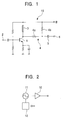
- FIG. 1 is a circuit diagram of a buffer amplifier according to an embodiment of the present invention;
- FIG. 2 is a block diagram illustrating an electronic circuit unit according to an embodiment of the present invention;
- FIG. 3 is an exploded perspective view of the electronic circuit unit of the present invention; and
- FIG. 4 is a circuit diagram of a buffer amplifier of the related art.
-
- A circuit configuration of a buffer amplifier according to an embodiment of the present invention will now be described with reference to FIG. 1. In a
buffer amplifier 10, an amplifyingtransistor 1 is biased so as to operate at a predetermined operating point as an amplifying device with the emitter thereof being grounded. The amplifyingtransistor 1 has a base connected to aninput terminal 2 and has a collector to which power is fed from a power supply B through aninductance element 3. The collector is also connected to aresistance attenuator 4. - The
resistance attenuator 4 of this embodiment is formed as an asymmetrical attenuator having a pair ofresistances resistance 4a serves as an input end, the other end of theresistance 4b is a ground end, and the node is an output end. The input end is directly connected to the collector of the amplifyingtransistor 1, and the ground end is connected to the power supply B. The output end is connected to anoutput terminal 6 through acoupling capacitor 5. Theresistance attenuator 4 may also be formed of a symmetrical attenuator with a T-shape, a π-shape, or the like. - In the configuration described above, the
resistance attenuator 4 is not necessarily used for impedance transformation or impedance matching, but is intended primarily for level setting of a signal. Thecoupling capacitor 5 has an impedance matching function and also serves a DC-blocking capacitor, along with theinductance element 3. - For example, the
buffer amplifier 10 having the configuration described above is configured as an electronic circuit unit in conjunction with a voltage-controlled oscillator and the like for use in a portable telephone. FIG. 2 illustrates the circuit configuration of an electronic circuit unit according to an embodiment of the present invention. This electronic circuit unit is configured as a frequency synthesizer, which includes thebuffer amplifier 10, a voltage-controlledoscillator 11 for supplying a signal, and a PLL (phase-locked loop)circuit 12 for controlling the oscillation frequency of the voltage-controlledoscillator 11. - An oscillation signal output from the voltage-controlled
oscillator 11 is amplified by the amplifyingtransistor 1 of thebuffer amplifier 10, and is further set to a predetermined level by theresistance attenuator 4. This level setting is performed by suitably setting the resistance values of theresistances - FIG. 3 is an exploded perspective view of the frequency synthesizer. Circuit elements mounted on a printed
circuit board 13 constitute thebuffer amplifier 10, the voltage-controlledoscillator 11, thePLL circuit 12, and the like.Terminal electrodes circuit board 13 and are connected with thebuffer amplifier 10, the voltage-controlledoscillator 11, thePLL circuit 12, and the like. Acover 14 is also installed on the printedcircuit board 13 from above. The frequency synthesizer is then mounted on a motherboard (not shown), and theterminal electrodes
Claims (3)
- A buffer amplifier comprising:wherein the input end of said resistance attenuator is directly connected to the collector of said amplifying transistor, the ground end is connected to the power supply, and the output end of said resistance attenuator is connected to said output terminal through a coupling capacitor.an amplifying transistor;an inductance element for feeding power to a collector of said amplifying transistor from a power supply;a resistance attenuator having an input end, an output end, and a ground end; andan output terminal connected to said resistance attenuator,
- A buffer amplifier according to claim 1, wherein said resistance attenuator is formed of an L-shaped asymmetrical circuit.
- An electronic circuit unit comprising said buffer amplifier according to claim 1 and a voltage-controlled oscillator, wherein said buffer amplifier sets the level of an oscillation signal output from said voltage-controlled oscillator.
Applications Claiming Priority (2)
| Application Number | Priority Date | Filing Date | Title |
|---|---|---|---|
| JP2001068993A JP2002271151A (en) | 2001-03-12 | 2001-03-12 | Buffer amplifier and electronic circuit unit using the same |
| JP2001068993 | 2001-03-12 |
Publications (2)
| Publication Number | Publication Date |
|---|---|
| EP1244209A2 true EP1244209A2 (en) | 2002-09-25 |
| EP1244209A3 EP1244209A3 (en) | 2005-03-30 |
Family
ID=18927095
Family Applications (1)
| Application Number | Title | Priority Date | Filing Date |
|---|---|---|---|
| EP02250259A Withdrawn EP1244209A3 (en) | 2001-03-12 | 2002-01-15 | Miniaturized buffer amplifier and electronic circuit using same |
Country Status (5)
| Country | Link |
|---|---|
| US (1) | US6750708B2 (en) |
| EP (1) | EP1244209A3 (en) |
| JP (1) | JP2002271151A (en) |
| KR (1) | KR100434863B1 (en) |
| CN (1) | CN1375928A (en) |
Families Citing this family (2)
| Publication number | Priority date | Publication date | Assignee | Title |
|---|---|---|---|---|
| CN100442656C (en) * | 2003-10-21 | 2008-12-10 | 瑞昱半导体股份有限公司 | low noise amplifier and method for amplifying signal |
| TWI857400B (en) * | 2022-11-22 | 2024-10-01 | 宏碁股份有限公司 | Electronic device with speaker protection mechanism |
Family Cites Families (10)
| Publication number | Priority date | Publication date | Assignee | Title |
|---|---|---|---|---|
| US3973214A (en) * | 1975-01-20 | 1976-08-03 | Alpha Engineering Corporation | Circuit to achieve low noise figure |
| US4498052A (en) * | 1976-12-23 | 1985-02-05 | Her Majesty The Queen In Right Of Canada, As Represented By The Minister Of National Defence | Signal detecting circuit |
| JP3715335B2 (en) | 1994-06-21 | 2005-11-09 | ソニー株式会社 | PLL synthesizer circuit |
| KR960027387A (en) * | 1994-12-12 | 1996-07-22 | 구자홍 | Transmission output control device of communication device |
| JP3142220B2 (en) * | 1995-03-30 | 2001-03-07 | シャープ株式会社 | Tuner |
| US5726606A (en) * | 1996-07-17 | 1998-03-10 | Eagle Comtronics, Inc. | Pre-emphasis network with variable time delay |
| US6078794A (en) * | 1997-02-19 | 2000-06-20 | Motorola, Inc. | Impedance matching for a dual band power amplifier |
| US5914634A (en) * | 1997-09-17 | 1999-06-22 | Northern Telecom Limited | Multiple switchable input LNA with input impedance control |
| CA2238955A1 (en) * | 1998-05-26 | 1999-11-26 | Gyles Panther | Novel biasing scheme for gaasfet amplifier |
| US6522195B2 (en) * | 2000-12-07 | 2003-02-18 | Motorola, Inc. | Low noise amplifier having bypass circuitry |
-
2001
- 2001-03-12 JP JP2001068993A patent/JP2002271151A/en not_active Withdrawn
-
2002
- 2002-01-15 EP EP02250259A patent/EP1244209A3/en not_active Withdrawn
- 2002-03-11 KR KR10-2002-0012870A patent/KR100434863B1/en not_active Expired - Fee Related
- 2002-03-11 US US10/095,888 patent/US6750708B2/en not_active Expired - Fee Related
- 2002-03-12 CN CN02106989A patent/CN1375928A/en active Pending
Non-Patent Citations (1)
| Title |
|---|
| None * |
Also Published As
| Publication number | Publication date |
|---|---|
| CN1375928A (en) | 2002-10-23 |
| EP1244209A3 (en) | 2005-03-30 |
| US6750708B2 (en) | 2004-06-15 |
| KR20020072792A (en) | 2002-09-18 |
| KR100434863B1 (en) | 2004-06-07 |
| US20020125946A1 (en) | 2002-09-12 |
| JP2002271151A (en) | 2002-09-20 |
Similar Documents
| Publication | Publication Date | Title |
|---|---|---|
| EP1231674A3 (en) | Antenna device | |
| KR930001293B1 (en) | High Frequency Power Amplifier | |
| JPH08148933A (en) | Voltage controlled oscillator | |
| US6163222A (en) | Buffer amplifier with frequency selective mechanism | |
| US6750708B2 (en) | Miniaturized buffer amplifier and electronic circuit unit using same | |
| US6104255A (en) | Voltage controlled oscillator with a resonator common to a resonance circuit and an oscillation circuit and a capacitor | |
| US6836190B2 (en) | Oscillator device and electronic apparatus using the same | |
| EP1079513A1 (en) | Oscillating apparatus including two-band resonance circuit | |
| JP3498608B2 (en) | PLL circuit, communication device using the same, and frequency adjustment method for PLL circuit | |
| JP3409061B2 (en) | Piezoelectric oscillator | |
| EP1096664B1 (en) | Oscillator with buffer circuit in which deterioration in c/n ration is lightened | |
| JP2003298334A (en) | Dielectric antenna device and electronic apparatus having dielectric antenna device | |
| JP2001339240A (en) | Voltage controlled oscillator | |
| JP2001160714A (en) | Oscillator | |
| US7205856B2 (en) | Piezoelectric oscillator | |
| JPH06338741A (en) | Transistor amplifier | |
| JP2000216641A (en) | Power amplifier | |
| JP2003060434A (en) | Oscillator and electronic apparatus using the same | |
| JP2000216633A (en) | Voltage controlled crystal oscillator | |
| JPH09162641A (en) | Voltage control oscillator | |
| JP2003017936A (en) | Voltage controlled oscillator | |
| JP2001237647A (en) | High frequency power amplifier | |
| JP3491562B2 (en) | Frequency multiplier | |
| JPH1146123A (en) | High frequency amplifier | |
| JPS58201432A (en) | radio receiver |
Legal Events
| Date | Code | Title | Description |
|---|---|---|---|
| PUAI | Public reference made under article 153(3) epc to a published international application that has entered the european phase |
Free format text: ORIGINAL CODE: 0009012 |
|
| AK | Designated contracting states |
Kind code of ref document: A2 Designated state(s): AT BE CH CY DE DK ES FI FR GB GR IE IT LI LU MC NL PT SE TR |
|
| AX | Request for extension of the european patent |
Free format text: AL;LT;LV;MK;RO;SI |
|
| PUAL | Search report despatched |
Free format text: ORIGINAL CODE: 0009013 |
|
| AK | Designated contracting states |
Kind code of ref document: A3 Designated state(s): AT BE CH CY DE DK ES FI FR GB GR IE IT LI LU MC NL PT SE TR |
|
| AX | Request for extension of the european patent |
Extension state: AL LT LV MK RO SI |
|
| 17P | Request for examination filed |
Effective date: 20050408 |
|
| AKX | Designation fees paid |
Designated state(s): DE FI FR GB |
|
| 17Q | First examination report despatched |
Effective date: 20061221 |
|
| STAA | Information on the status of an ep patent application or granted ep patent |
Free format text: STATUS: THE APPLICATION IS DEEMED TO BE WITHDRAWN |
|
| 18D | Application deemed to be withdrawn |
Effective date: 20070503 |