EP1244089A2 - Self-emission display device and method for driving the same - Google Patents
Self-emission display device and method for driving the same Download PDFInfo
- Publication number
- EP1244089A2 EP1244089A2 EP02252020A EP02252020A EP1244089A2 EP 1244089 A2 EP1244089 A2 EP 1244089A2 EP 02252020 A EP02252020 A EP 02252020A EP 02252020 A EP02252020 A EP 02252020A EP 1244089 A2 EP1244089 A2 EP 1244089A2
- Authority
- EP
- European Patent Office
- Prior art keywords
- light emitting
- emitting elements
- display device
- scrs
- emission display
- Prior art date
- Legal status (The legal status is an assumption and is not a legal conclusion. Google has not performed a legal analysis and makes no representation as to the accuracy of the status listed.)
- Withdrawn
Links
- 238000000034 method Methods 0.000 title claims description 62
- 239000011159 matrix material Substances 0.000 claims abstract description 40
- 230000003068 static effect Effects 0.000 claims description 9
- 230000002459 sustained effect Effects 0.000 claims description 6
- 230000003247 decreasing effect Effects 0.000 claims description 3
- 238000004519 manufacturing process Methods 0.000 description 14
- 238000010276 construction Methods 0.000 description 12
- 239000000758 substrate Substances 0.000 description 5
- XUIMIQQOPSSXEZ-UHFFFAOYSA-N Silicon Chemical compound [Si] XUIMIQQOPSSXEZ-UHFFFAOYSA-N 0.000 description 4
- 230000008020 evaporation Effects 0.000 description 4
- 238000001704 evaporation Methods 0.000 description 4
- 230000006870 function Effects 0.000 description 4
- 229910052710 silicon Inorganic materials 0.000 description 4
- 239000010703 silicon Substances 0.000 description 4
- 230000000694 effects Effects 0.000 description 3
- 238000005286 illumination Methods 0.000 description 3
- 238000012545 processing Methods 0.000 description 2
- 239000002131 composite material Substances 0.000 description 1
- 238000010586 diagram Methods 0.000 description 1
- 239000007772 electrode material Substances 0.000 description 1
- 238000005516 engineering process Methods 0.000 description 1
- 238000011160 research Methods 0.000 description 1
- 238000012827 research and development Methods 0.000 description 1
- 239000010409 thin film Substances 0.000 description 1
- 238000012546 transfer Methods 0.000 description 1
Images





Classifications
-
- G—PHYSICS
- G09—EDUCATION; CRYPTOGRAPHY; DISPLAY; ADVERTISING; SEALS
- G09G—ARRANGEMENTS OR CIRCUITS FOR CONTROL OF INDICATING DEVICES USING STATIC MEANS TO PRESENT VARIABLE INFORMATION
- G09G3/00—Control arrangements or circuits, of interest only in connection with visual indicators other than cathode-ray tubes
- G09G3/20—Control arrangements or circuits, of interest only in connection with visual indicators other than cathode-ray tubes for presentation of an assembly of a number of characters, e.g. a page, by composing the assembly by combination of individual elements arranged in a matrix no fixed position being assigned to or needed to be assigned to the individual characters or partial characters
- G09G3/22—Control arrangements or circuits, of interest only in connection with visual indicators other than cathode-ray tubes for presentation of an assembly of a number of characters, e.g. a page, by composing the assembly by combination of individual elements arranged in a matrix no fixed position being assigned to or needed to be assigned to the individual characters or partial characters using controlled light sources
- G09G3/30—Control arrangements or circuits, of interest only in connection with visual indicators other than cathode-ray tubes for presentation of an assembly of a number of characters, e.g. a page, by composing the assembly by combination of individual elements arranged in a matrix no fixed position being assigned to or needed to be assigned to the individual characters or partial characters using controlled light sources using electroluminescent panels
- G09G3/32—Control arrangements or circuits, of interest only in connection with visual indicators other than cathode-ray tubes for presentation of an assembly of a number of characters, e.g. a page, by composing the assembly by combination of individual elements arranged in a matrix no fixed position being assigned to or needed to be assigned to the individual characters or partial characters using controlled light sources using electroluminescent panels semiconductive, e.g. using light-emitting diodes [LED]
- G09G3/3208—Control arrangements or circuits, of interest only in connection with visual indicators other than cathode-ray tubes for presentation of an assembly of a number of characters, e.g. a page, by composing the assembly by combination of individual elements arranged in a matrix no fixed position being assigned to or needed to be assigned to the individual characters or partial characters using controlled light sources using electroluminescent panels semiconductive, e.g. using light-emitting diodes [LED] organic, e.g. using organic light-emitting diodes [OLED]
- G09G3/3216—Control arrangements or circuits, of interest only in connection with visual indicators other than cathode-ray tubes for presentation of an assembly of a number of characters, e.g. a page, by composing the assembly by combination of individual elements arranged in a matrix no fixed position being assigned to or needed to be assigned to the individual characters or partial characters using controlled light sources using electroluminescent panels semiconductive, e.g. using light-emitting diodes [LED] organic, e.g. using organic light-emitting diodes [OLED] using a passive matrix
-
- G—PHYSICS
- G09—EDUCATION; CRYPTOGRAPHY; DISPLAY; ADVERTISING; SEALS
- G09G—ARRANGEMENTS OR CIRCUITS FOR CONTROL OF INDICATING DEVICES USING STATIC MEANS TO PRESENT VARIABLE INFORMATION
- G09G3/00—Control arrangements or circuits, of interest only in connection with visual indicators other than cathode-ray tubes
- G09G3/20—Control arrangements or circuits, of interest only in connection with visual indicators other than cathode-ray tubes for presentation of an assembly of a number of characters, e.g. a page, by composing the assembly by combination of individual elements arranged in a matrix no fixed position being assigned to or needed to be assigned to the individual characters or partial characters
- G09G3/22—Control arrangements or circuits, of interest only in connection with visual indicators other than cathode-ray tubes for presentation of an assembly of a number of characters, e.g. a page, by composing the assembly by combination of individual elements arranged in a matrix no fixed position being assigned to or needed to be assigned to the individual characters or partial characters using controlled light sources
- G09G3/30—Control arrangements or circuits, of interest only in connection with visual indicators other than cathode-ray tubes for presentation of an assembly of a number of characters, e.g. a page, by composing the assembly by combination of individual elements arranged in a matrix no fixed position being assigned to or needed to be assigned to the individual characters or partial characters using controlled light sources using electroluminescent panels
- G09G3/32—Control arrangements or circuits, of interest only in connection with visual indicators other than cathode-ray tubes for presentation of an assembly of a number of characters, e.g. a page, by composing the assembly by combination of individual elements arranged in a matrix no fixed position being assigned to or needed to be assigned to the individual characters or partial characters using controlled light sources using electroluminescent panels semiconductive, e.g. using light-emitting diodes [LED]
- G09G3/3208—Control arrangements or circuits, of interest only in connection with visual indicators other than cathode-ray tubes for presentation of an assembly of a number of characters, e.g. a page, by composing the assembly by combination of individual elements arranged in a matrix no fixed position being assigned to or needed to be assigned to the individual characters or partial characters using controlled light sources using electroluminescent panels semiconductive, e.g. using light-emitting diodes [LED] organic, e.g. using organic light-emitting diodes [OLED]
- G09G3/3225—Control arrangements or circuits, of interest only in connection with visual indicators other than cathode-ray tubes for presentation of an assembly of a number of characters, e.g. a page, by composing the assembly by combination of individual elements arranged in a matrix no fixed position being assigned to or needed to be assigned to the individual characters or partial characters using controlled light sources using electroluminescent panels semiconductive, e.g. using light-emitting diodes [LED] organic, e.g. using organic light-emitting diodes [OLED] using an active matrix
- G09G3/3233—Control arrangements or circuits, of interest only in connection with visual indicators other than cathode-ray tubes for presentation of an assembly of a number of characters, e.g. a page, by composing the assembly by combination of individual elements arranged in a matrix no fixed position being assigned to or needed to be assigned to the individual characters or partial characters using controlled light sources using electroluminescent panels semiconductive, e.g. using light-emitting diodes [LED] organic, e.g. using organic light-emitting diodes [OLED] using an active matrix with pixel circuitry controlling the current through the light-emitting element
-
- G—PHYSICS
- G09—EDUCATION; CRYPTOGRAPHY; DISPLAY; ADVERTISING; SEALS
- G09G—ARRANGEMENTS OR CIRCUITS FOR CONTROL OF INDICATING DEVICES USING STATIC MEANS TO PRESENT VARIABLE INFORMATION
- G09G3/00—Control arrangements or circuits, of interest only in connection with visual indicators other than cathode-ray tubes
- G09G3/20—Control arrangements or circuits, of interest only in connection with visual indicators other than cathode-ray tubes for presentation of an assembly of a number of characters, e.g. a page, by composing the assembly by combination of individual elements arranged in a matrix no fixed position being assigned to or needed to be assigned to the individual characters or partial characters
- G09G3/22—Control arrangements or circuits, of interest only in connection with visual indicators other than cathode-ray tubes for presentation of an assembly of a number of characters, e.g. a page, by composing the assembly by combination of individual elements arranged in a matrix no fixed position being assigned to or needed to be assigned to the individual characters or partial characters using controlled light sources
- G09G3/30—Control arrangements or circuits, of interest only in connection with visual indicators other than cathode-ray tubes for presentation of an assembly of a number of characters, e.g. a page, by composing the assembly by combination of individual elements arranged in a matrix no fixed position being assigned to or needed to be assigned to the individual characters or partial characters using controlled light sources using electroluminescent panels
- G09G3/32—Control arrangements or circuits, of interest only in connection with visual indicators other than cathode-ray tubes for presentation of an assembly of a number of characters, e.g. a page, by composing the assembly by combination of individual elements arranged in a matrix no fixed position being assigned to or needed to be assigned to the individual characters or partial characters using controlled light sources using electroluminescent panels semiconductive, e.g. using light-emitting diodes [LED]
- G09G3/3208—Control arrangements or circuits, of interest only in connection with visual indicators other than cathode-ray tubes for presentation of an assembly of a number of characters, e.g. a page, by composing the assembly by combination of individual elements arranged in a matrix no fixed position being assigned to or needed to be assigned to the individual characters or partial characters using controlled light sources using electroluminescent panels semiconductive, e.g. using light-emitting diodes [LED] organic, e.g. using organic light-emitting diodes [OLED]
- G09G3/3266—Details of drivers for scan electrodes
-
- G—PHYSICS
- G09—EDUCATION; CRYPTOGRAPHY; DISPLAY; ADVERTISING; SEALS
- G09G—ARRANGEMENTS OR CIRCUITS FOR CONTROL OF INDICATING DEVICES USING STATIC MEANS TO PRESENT VARIABLE INFORMATION
- G09G3/00—Control arrangements or circuits, of interest only in connection with visual indicators other than cathode-ray tubes
- G09G3/20—Control arrangements or circuits, of interest only in connection with visual indicators other than cathode-ray tubes for presentation of an assembly of a number of characters, e.g. a page, by composing the assembly by combination of individual elements arranged in a matrix no fixed position being assigned to or needed to be assigned to the individual characters or partial characters
- G09G3/22—Control arrangements or circuits, of interest only in connection with visual indicators other than cathode-ray tubes for presentation of an assembly of a number of characters, e.g. a page, by composing the assembly by combination of individual elements arranged in a matrix no fixed position being assigned to or needed to be assigned to the individual characters or partial characters using controlled light sources
- G09G3/30—Control arrangements or circuits, of interest only in connection with visual indicators other than cathode-ray tubes for presentation of an assembly of a number of characters, e.g. a page, by composing the assembly by combination of individual elements arranged in a matrix no fixed position being assigned to or needed to be assigned to the individual characters or partial characters using controlled light sources using electroluminescent panels
- G09G3/32—Control arrangements or circuits, of interest only in connection with visual indicators other than cathode-ray tubes for presentation of an assembly of a number of characters, e.g. a page, by composing the assembly by combination of individual elements arranged in a matrix no fixed position being assigned to or needed to be assigned to the individual characters or partial characters using controlled light sources using electroluminescent panels semiconductive, e.g. using light-emitting diodes [LED]
- G09G3/3208—Control arrangements or circuits, of interest only in connection with visual indicators other than cathode-ray tubes for presentation of an assembly of a number of characters, e.g. a page, by composing the assembly by combination of individual elements arranged in a matrix no fixed position being assigned to or needed to be assigned to the individual characters or partial characters using controlled light sources using electroluminescent panels semiconductive, e.g. using light-emitting diodes [LED] organic, e.g. using organic light-emitting diodes [OLED]
- G09G3/3275—Details of drivers for data electrodes
-
- G—PHYSICS
- G09—EDUCATION; CRYPTOGRAPHY; DISPLAY; ADVERTISING; SEALS
- G09G—ARRANGEMENTS OR CIRCUITS FOR CONTROL OF INDICATING DEVICES USING STATIC MEANS TO PRESENT VARIABLE INFORMATION
- G09G2300/00—Aspects of the constitution of display devices
- G09G2300/08—Active matrix structure, i.e. with use of active elements, inclusive of non-linear two terminal elements, in the pixels together with light emitting or modulating elements
-
- G—PHYSICS
- G09—EDUCATION; CRYPTOGRAPHY; DISPLAY; ADVERTISING; SEALS
- G09G—ARRANGEMENTS OR CIRCUITS FOR CONTROL OF INDICATING DEVICES USING STATIC MEANS TO PRESENT VARIABLE INFORMATION
- G09G2300/00—Aspects of the constitution of display devices
- G09G2300/08—Active matrix structure, i.e. with use of active elements, inclusive of non-linear two terminal elements, in the pixels together with light emitting or modulating elements
- G09G2300/088—Active matrix structure, i.e. with use of active elements, inclusive of non-linear two terminal elements, in the pixels together with light emitting or modulating elements using a non-linear two-terminal element
-
- G—PHYSICS
- G09—EDUCATION; CRYPTOGRAPHY; DISPLAY; ADVERTISING; SEALS
- G09G—ARRANGEMENTS OR CIRCUITS FOR CONTROL OF INDICATING DEVICES USING STATIC MEANS TO PRESENT VARIABLE INFORMATION
- G09G2310/00—Command of the display device
- G09G2310/06—Details of flat display driving waveforms
-
- G—PHYSICS
- G09—EDUCATION; CRYPTOGRAPHY; DISPLAY; ADVERTISING; SEALS
- G09G—ARRANGEMENTS OR CIRCUITS FOR CONTROL OF INDICATING DEVICES USING STATIC MEANS TO PRESENT VARIABLE INFORMATION
- G09G2320/00—Control of display operating conditions
- G09G2320/06—Adjustment of display parameters
- G09G2320/0606—Manual adjustment
-
- G—PHYSICS
- G09—EDUCATION; CRYPTOGRAPHY; DISPLAY; ADVERTISING; SEALS
- G09G—ARRANGEMENTS OR CIRCUITS FOR CONTROL OF INDICATING DEVICES USING STATIC MEANS TO PRESENT VARIABLE INFORMATION
- G09G2320/00—Control of display operating conditions
- G09G2320/06—Adjustment of display parameters
- G09G2320/0626—Adjustment of display parameters for control of overall brightness
-
- G—PHYSICS
- G09—EDUCATION; CRYPTOGRAPHY; DISPLAY; ADVERTISING; SEALS
- G09G—ARRANGEMENTS OR CIRCUITS FOR CONTROL OF INDICATING DEVICES USING STATIC MEANS TO PRESENT VARIABLE INFORMATION
- G09G3/00—Control arrangements or circuits, of interest only in connection with visual indicators other than cathode-ray tubes
- G09G3/20—Control arrangements or circuits, of interest only in connection with visual indicators other than cathode-ray tubes for presentation of an assembly of a number of characters, e.g. a page, by composing the assembly by combination of individual elements arranged in a matrix no fixed position being assigned to or needed to be assigned to the individual characters or partial characters
- G09G3/22—Control arrangements or circuits, of interest only in connection with visual indicators other than cathode-ray tubes for presentation of an assembly of a number of characters, e.g. a page, by composing the assembly by combination of individual elements arranged in a matrix no fixed position being assigned to or needed to be assigned to the individual characters or partial characters using controlled light sources
- G09G3/30—Control arrangements or circuits, of interest only in connection with visual indicators other than cathode-ray tubes for presentation of an assembly of a number of characters, e.g. a page, by composing the assembly by combination of individual elements arranged in a matrix no fixed position being assigned to or needed to be assigned to the individual characters or partial characters using controlled light sources using electroluminescent panels
- G09G3/32—Control arrangements or circuits, of interest only in connection with visual indicators other than cathode-ray tubes for presentation of an assembly of a number of characters, e.g. a page, by composing the assembly by combination of individual elements arranged in a matrix no fixed position being assigned to or needed to be assigned to the individual characters or partial characters using controlled light sources using electroluminescent panels semiconductive, e.g. using light-emitting diodes [LED]
-
- H—ELECTRICITY
- H10—SEMICONDUCTOR DEVICES; ELECTRIC SOLID-STATE DEVICES NOT OTHERWISE PROVIDED FOR
- H10K—ORGANIC ELECTRIC SOLID-STATE DEVICES
- H10K50/00—Organic light-emitting devices
- H10K50/80—Constructional details
- H10K50/805—Electrodes
- H10K50/82—Cathodes
- H10K50/828—Transparent cathodes, e.g. comprising thin metal layers
-
- H—ELECTRICITY
- H10—SEMICONDUCTOR DEVICES; ELECTRIC SOLID-STATE DEVICES NOT OTHERWISE PROVIDED FOR
- H10K—ORGANIC ELECTRIC SOLID-STATE DEVICES
- H10K59/00—Integrated devices, or assemblies of multiple devices, comprising at least one organic light-emitting element covered by group H10K50/00
- H10K59/10—OLED displays
- H10K59/12—Active-matrix OLED [AMOLED] displays
Definitions
- the present invention relates to such display device and method for driving the same that uses a current-control type self-emission element such as an organic electro-luminescent (EL) element or a light emitting diode (LED).
- a current-control type self-emission element such as an organic electro-luminescent (EL) element or a light emitting diode (LED).
- this type of a practical display device has typically employed a passive matrix driving method.
- the passive matrix driving method By the passive matrix driving method, however, an instantaneous current and a driving voltage both rise remarkably in a high duty-ratio driving period, thus inevitably restricting the number of scan electrodes that can be driven at a time. It is, therefore, difficult to employ the passive matrix driving method to realize a relatively high-definition display device that requires a few hundreds of scan electrodes.
- a switching element driving element
- TFT thin film transistor
- the thyrister itself is controlled in driving by controlling a voltage applied across, so that, as described in such a specification, an organic EL element will be lit up, even if a little (4.5 cd/m 2 ), as against illumination thereof (100 cd/m 2 ) even in a period for which it must not be lit up.
- a self emission display device for controlling a lit-up/non-lit-up state of a light emitting element by controlling a current flowing therethrough provided with: a plurality of light emitting elements arrayed in a matrix; and a plurality of SCRs for controlling a current flowing through the light emitting elements, corresponding to each of the light emitting elements; wherein each of the light emitting elements is connected to an anode in each of the SCRs.
- a silicon controlled rectifier is used in configuration as the driving element to provide an optimal driving method, so that it is possible to realize active driving of a high-performance self emission display excellent in numeric aperture, contrast, etc. with a relatively simple configuration.
- the SCR can be formed by an extremely simple manufacturing process, that is, it can formed as stacked on a stack type light emitting element by almost the same manufacturing process including evaporation as that for the light emitting element, thus also reducing the costs for manufacture.
- the light emitting elements are organic EL elements.
- the light emitting elements are light emitting diodes.
- a ratio in static capacity between the SCR and the light emitting element is adjusted to thereby optimize a ratio of a voltage applied to the SCR and a voltage applied to the light emitting element in a non-conducting state.
- the self emission display device has a control device to set a current value that corresponds to a target brightness based on a current vs. brightness characteristic of the light emitting element to thereby set an optimal source voltage that corresponds to the set current value based on voltage vs. current characteristics of both the SCR and the light emitting element.
- a target brightness can be obtained easily.
- the lit-up/non-lit-up states of each of the light emitting elements are determined by a voltage value applied to a gate in each of the SCRs.
- a break-over voltage in each of the SCRs is determined by a voltage value applied to a gate in each of the SCRs, the light emitting element is lighted up by decreasing the break-over voltage.
- a self emission display device for controlling a lit-up/non-lit-up state of a light emitting element by controlling a current flowing therethrough provided with: a plurality of light emitting elements arrayed in a matrix; and a plurality of SCRs for controlling a current flowing through the light emitting elements, corresponding to each of the light emitting elements; wherein each of the light emitting elements is connected to a cathode in each of the SCRs.
- a silicon controlled rectifier is used in configuration as the driving element to provide an optimal driving method, so that it is possible to realize active driving of a high-performance self emission display excellent in numeric aperture, contrast, etc. with a relatively simple configuration
- the SCR can be formed by an extremely simple manufacturing process, that is, it can formed as stacked on a stack type light emitting element by almost the same manufacturing process including evaporation as that for the light emitting element, thus also reducing the costs for manufacture.
- a self emission display device for controlling a lit-up/non-lit-up state of a light emitting element by controlling a current flowing therethrough provided with a plurality of light emitting elements arrayed in a matrix; wherein the light emitting elements are light emitting SCRs.
- the above object of the present invention can be achieved by a method for driving a self emission display device having a plurality of light emitting elements arrayed in a matrix and a plurality of SCRs for controlling a current flowing through the light emitting elements, wherein each of the light emitting elements is connected to an anode in each of the SCRs, provided with: a process of scanning sequentially each of the SCRs; and a process of driving each of the SCRs so that each of the light emitting elements be sustained in a conducting or non-conducting state.
- a silicon controlled rectifier is used as the driving element to provide an optimal driving method, so that it is possible to realize active driving of a high-performance self emission display excellent in numeric aperture, contrast, etc. with a relatively simple configuration.
- the light emitting elements are organic EL elements.
- the light emitting elements are light emitting diodes.
- a ratio in static capacity between the SCR and the light emitting element is adjusted to thereby optimize a ratio of a voltage applied to the SCR and a voltage applied to the light emitting element in a non-conducting state.
- the method comprises: a process of setting a current value that corresponds to a target brightness based on a current vs. brightness characteristic of the light emitting element; and a process of setting an optimal source voltage that corresponds to the set current value based on voltage vs. current characteristics of both the SCR and the light emitting element.
- a target brightness can be obtained easily.
- each of the SCRs are of a P-gate type, each of the gates of which are connected to a common gate switch that can switch over a high potential and a low potential for each column in a matrix, each of the anodes of which are connected via their respective ones of the light emitting elements to a common power source, and each of the cathodes of which are connected for each row thereof in the matrix to a common scan switch that can switch over a high potential, a low potential, and an intermediate potential; when each of the light emitting elements is in a non-selected period, the corresponding one of the gate switches is set to the high potential and the corresponding one of the scan switches is set to the intermediate potential; and when each of the light emitting elements is in a selected period, the corresponding one of the scan switches is set to the high potential and then to the low potential and, to light up any one of the light emitting element, the corresponding one of the gate switches is set to the high potential in a
- each of the SCRs are of an N-gate type, each of the gates of which are connected to a common gate switch that can switch over a high potential and a low potential for each column in a matrix, each of the cathodes of which are connected via their respective ones of the light emitting elements to a common power source, and each of the anodes of which are connected for each row thereof in the matrix to a common scan switch that can switch over a high potential, a low potential, and an intermediate potential; when each of the light emitting elements is in a non-selected period, the corresponding one of the gate switches is set to the high potential and the corresponding one of the scan switches is set to the intermediate potential; and when each of the light emitting elements is in a selected period, the corresponding one of the scan switches is set to the high potential and then to the low potential and, to light up any one of the light emitting element, the corresponding one of the gate switches is set to the low potential in a period
- the above object of the present invention can be achieved by a method for driving a self emission display device having a plurality of light emitting elements arrayed in a matrix and a plurality of SCRs for controlling a current flowing through the light emitting elements, wherein each of the light emitting elements is connected to a cathode in each of the SCRs, provided with: a process of scanning sequentially each of the SCRs; and a process of driving each of the SCRs so that each of the light emitting elements be sustained in a conducting or non-conducting state.
- a silicon controlled rectifier is used as the driving element to provide an optimal driving method, so that it is possible to realize active driving of a high-performance self emission display excellent in numeric aperture, contrast, etc. with a relatively simple configuration.
- the above object of the present invention can be achieved by a method for driving a self emission display device having a plurality of light emitting elements arrayed in a matrix and a plurality of SCRs for controlling a current flowing through the light emitting elements, provided with: a process of scanning sequentially each of the SCRs to provide each of the light emitting elements with a selected period in which a lit-up/non-lit-up state of the light emitting elements is determined; and a process of applying a predetermined voltage to a gate of the corresponding one of the SCRs in the selected period to light up any of the light emitting elements.
- the present invention by switching a voltage applied at the gate of an SCR, it is possible to securely light up a light emitting diode in a period during which it must be in the lit-up state and not to light it up securely in a period during which it must be in the non-lit-up state, thus realizing a sufficiently good contrast.
- a method for driving a self emission display device having a plurality of light emitting elements arrayed in a matrix, wherein the light emitting elements are light emitting SCRs provide with: a process of scanning sequentially each of the light emitting SCRs; and a process of driving each of the light emitting SCRs so that each of the light emitting SCRs be sustained in a conducting or non-conducting state.
- FIG. 1 shows a schematic configuration of the organic EL display device according to this embodiment.
- the organic EL display device 100 comprises: an organic EL display 1 including a plurality of organic EL elements arrayed in a matrix and a plurality of SCRs for controlling a current flowing through these organic EL elements; and a display control section 2 as a control device for using the SCRs in active matrix driving.
- This embodiment combines the organic EL elements acting as a light emitting element and the SCRs acting as a driving element to thereby realize optimal active matrix driving.
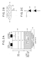
- FIG. 2A shows an example of an element configuration of an organic EL element and an SCR element.
- an organic EL element 20 is stacked on an anode electrode 10 realized as such a transparent electrode formed on a transparent substrate that is made of a transparent electrode material such as ITO.
- an SCR 30 On this organic EL element 20 is stacked an SCR 30, to be connected with an anode A in the SCR 30.
- the SCR 30 is of a P-gate type such as shown in FIG. 2B.
- a gate G of the SCR 30 is formed a gate electrode 40, while at a cathode K of the SCR 30 is formed a cathode electrode 50.
- FIG. 2C is an equivalent circuit of the element construction of FIG. 2A.
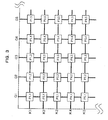
- stacked organic EL element 20 and SCR 30 are arrayed in a matrix (P1,1, P1,2, ...) as shown in FIG. 3, thus forming the organic EL display 1.
- FIG. 4 is an illustration for showing an example of a circuit connection configuration having an organic EL display 1 comprised of organic EL elements 20 and SCRs 30 arrayed in a matrix, a group of scan switches (SWs), a group of gate (signal) switches (SWs), etc.
- the anode electrodes 10 of the organic EL elements 20 are connected to a common power source
- the gate electrodes 40 of the SCRs 30 in each column are connected to the corresponding one of common signals SWn, SWn+1, SWn+2, ...
- the cathode electrode 50 of the SCRs 30 in each row are connected to the corresponding one of common scan signals SWm, SWm+1, SWm+2, ....
- the display control section 2 includes a CPU and a composite logic circuit having an operation function and also a memory etc., thus having a function to transfer display data etc. with an external device and then analyze and convert it into matrix data to be displayed at a predetermined position on the organic EL display 1. If each organic EL element 20 at an intersection in the matrix is supposed to be dot data for each picture element, the display control section 2 outputs a switching instruction to give the dot coordinates to each signal SW and each scanning SW. Furthermore, the display control section 2 controls the value of a common voltage VA of the common power source.
- FIG. 5 is a timing chart for showing the driving signal for driving picture elements in an n'th column when m'th through (m+2)'th rows are being scanned in the circuit configuration of FIG. 4. Basically, it sequentially scans the rows to thereby determine lighting (illumination) or non-lighting (non-illumination) of each of the organic EL elements 20 in a selected row selecting a potential applied on the gate G of the SCR 30. In FIG. 5, the scan signals SWm through SWm+2 are held at the intermediate potential (V0) during a non-selected period.
- the scan signals SWm through SWm+2 first switch over to the high potential (Voff) to reset the lit-up state of each of the organic EL elements and then switches over to the low potential (Von) for lit-up state/non-lit-up state selection.
- a signal SWn corresponding to this organic EL element 20 must be held at the ON potential (V0). That is, when the gate G is set to the ON potential (V0) with the cathode K of the corresponding SCR 30 held at the low potential (Von), a potential difference (V0 - Von of, for example, 0.6V or higher) between the gate G and the cathode K causes a gate current IG to flow through the SCR 30, which causes the SCR 30 to break over and be turned ON, thus flowing a current between the anode A and the cathode K. This in turn causes a current to flow (conduct) also through the organic EL element 20 connected to that corresponding SCR 30, thus lighting up the organic EL element 20.
- a signal SWn corresponding to this organic EL element 20 must be set to the OFF potential (Von). That is, when the gate G is set to the OFF potential (Von) with the cathode K of the corresponding SCR30 held at the low potential (Von), no gate electrode flows because there is no potential difference between the gate G and the cathode K, so that the SCR 30 does not break over and stays in the OFF state, to thereby flow no current through the organic EL element 20 (non-conducting), thus avoiding lighting it up.
- FIG. 6 shows a relationship between a voltage applied between an anode A and a cathode K of the SCR 30 and the corresponding current.
- VB01 indicates a break-over voltage when the gate current IG of the SCR30 does not flow
- VB02 indicates a break-over voltage when the gate current IG of the SCR 30 flows.
- VSSET indicates a voltage applied between the anode A and the cathode K of the SCR 30 when the scanning SW is held at the low potential.
- the condition (voltage) of the SCR 30 breaking over can be decreased from VB01 to VB02, which is lower than VSSET, so that a current flows between the anode A and the cathode K of the SCR 30 to thereby light up the organic EL element 20.
- a control is conducted so that the SCR 30 may be caused to break over only in a period when the scanning SW is set to the low potential (Von) and the signal SW is set to the ON potential (V0), and the control is conducted so that the SCR 30 may be caused not to break over except for the period to flow no current at all through the organic EL elements 20. It is, therefore, possible not to light up the organic EL element 20 securely in a period during which it must be in the non-lit-up state, thus realizing a sufficiently good contrast.
- VSSET (VA - Von) - VELSET
- VSSET is determined by a ratio (CEL/CS) of static capacity between the organic EL element 20 and the SCR 30, it can be set at an appropriate value by adjusting this static capacity ratio, specifically by controlling the areas of the organic EL element 20 and the SCR 30, for example.
- VSOFF indicates a voltage applied between the anode A and the cathode K of the SCR 30 when the organic EL element 20 is in the non-lit-upstate in the non-selected period
- VSON indicates a voltage applied between the anode A and the cathode K of the SCR 30 when the organic EL element 20 is in the lit-up state.
- VSR indicates a voltage applied between the anode A and the cathode K of the SCR 30 in the high potential period of the scanning SW (that is, period during which the scanning SW is held at the high voltage (Voff)) so that the SCR 30 may be turned OFF (reset).
- VSOFF VA - VELOFF
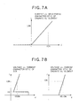
- FIG. 7A shows a current vs. brightness characteristic of the organic EL element 20.
- FIG. 7B shows a voltage vs. current characteristic of the organic EL element 20 and that of the SCR 30.
- FIG. 8 is a flowchart for showing processing by the display device control section 2 for setting the target brightness LON. Note here that these characteristics shown in FIG. 7 are stored in a memory in the display control section 2.
- the display control section 2 sets a target brightness LON based on an instruction sent from, for example, an external device (step S1).
- the display control section 2 determines a current value ION that corresponds to the target brightness LON based on the current vs. brightness characteristic of the organic EL element 20 shown in FIG. 7A (step S2).
- the display control section 2 determines voltage values of VSON and VELON corresponding to the ION value based on the voltage vs. current characteristics of both the organic EL element 20 and the SCR 30 shown in FIG. 7B (step S3).
- the display control section 2 then sums up the VSON and VELON values to determine a common voltage VA (step S4) and outputs a signal for setting at the VA value to the common power source (step S5).
- VA common voltage
- step S5 the value of VA determined at step S4 is supplied from the common power source to the organic EL element 1. It is thus possible to adjust the element characteristics so that a desired target brightness LON can be obtained.
- this embodiment has such a configuration that an SCR is used as an element for driving an organic EL element to thereby control the break-over voltage of the SCR for optimal driving, thus enabling realizing active driving of a high-performance organic EL display excellent in numeric aperture, contrast, etc. with a relatively simple construction.
- an extremely easy manufacturing process can be used, that is, an SCR can be stacked on a stack-type organic EL element using the same technology including evaporation as that for manufacture of the organic EL element, thus reducing the manufacturing costs.
- FIGS. 9 showing an example of an element construction according to another embodiment.
- the example of FIG. 9A has a light emitting SCR 200 construction that integrates therein the organic element 20 and the SCR 30, which are separated in FIG. 2A.
- FIG. 98 indicates an equivalent circuit of the element construction of the FIG . 9A.
- the light emitting SCR element array, connections, and driving method shown in FIGS. 9 are the same as those of the organic EL element 20 plus SCR 30 construction shown in FIG. 2.
- a self emission display can be manufactured by even simpler construction than the organic EL element 20 plus SCR 30 construction.
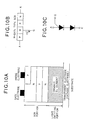
- an N-gate type SCR such as shown in FIG. 10 may be applied (in this case, the anode A and the cathode K are reversed in function), to obtain the same effects as those by the above embodiments.
- an N-gate type light emitting SCR may be used to obtain the same effects.
- the electrode opposite the substrate may be used as the transparent electrode to thereby emit light to the side opposite to the substrate, thus obtaining the same effects.
- the present invention is not limited thereto; for example, any other self emission element may be used such as a light emitting diode (LED).
- LED light emitting diode
Landscapes
- Engineering & Computer Science (AREA)
- Physics & Mathematics (AREA)
- Computer Hardware Design (AREA)
- General Physics & Mathematics (AREA)
- Theoretical Computer Science (AREA)
- Control Of Indicators Other Than Cathode Ray Tubes (AREA)
- Electroluminescent Light Sources (AREA)
- Devices For Indicating Variable Information By Combining Individual Elements (AREA)
- Control Of El Displays (AREA)
- Thyristors (AREA)
- Led Devices (AREA)
Abstract
Description
Claims (19)
- A self emission display device for controlling a lit-up/non-lit-up state of a light emitting element by controlling a current flowing therethrough, characterized in that the self emission display device(100) comprises:wherein each of the light emitting elements(20) is connected to an anode in each of the SCRs (30).a plurality of light emitting elements (20) arrayed in a matrix; anda plurality of SCRs(30) for controlling a current flowing through the light emitting elements(20), corresponding to each of the light emitting elements(20);
- A self emission display device for controlling a lit-up/non-lit-up state of a light emitting element by controlling a current flowing therethrough, characterized in that the self emission display device(100) comprises:wherein each of the light emitting elements(20) is connected to a cathode in each of the SCRs (30).a plurality of light emitting elements (20) arrayed in a matrix; anda plurality of SCRs(30) for controlling a current flowing through the light emitting elements(20), corresponding to each of the light emitting elements(20);
- The self emission display device (100) according to claim 1 or 2, wherein the light emitting elements (20) are organic EL elements.
- The self emission display device (100) according to claim 1 or 2, wherein the light emitting elements (20) are light emitting diodes.
- The self emission display device(100) according to any one of claims 1 to 4, wherein a ratio in static capacity between the SCR(30) and the light emitting element(20) is adjusted to thereby optimize a ratio of a voltage applied to the SCR(30) and a voltage applied to the light emitting element(20) in a non-conducting state.
- The self emission display device(100) according to any one of claims 1 to 5, wherein the self emission display device (100) has a control device(2) to set a current value that corresponds to a target brightness based on a current vs. brightness characteristic of the light emitting element (20) to thereby set an optimal source voltage that corresponds to the set current value based on voltage vs. current characteristics of both the SCR(30) and the light emitting element(20).
- A self emission display device for controlling a lit-up/non-lit-up state of a light emitting element by controlling a current flowing therethrough, characterized in that the self emission display device(100) comprises:wherein the light emitting elements are light emitting SCRs(200).a plurality of light emitting elements arrayed in a matrix;
- The self emission display device(100) according to any one of claims 1 to 7, wherein the lit-up/non-lit-up states of each of the light emitting elements (20) are determined by a voltage value applied to a gate in each of the SCRs(30).
- The self emission display device(100) according to any one of claims 1 to 8, wherein a break-over voltage in each of the SCRs(30) is determined by a voltage value applied to a gate in each of the SCRs (30), the light emitting element (20) is lighted up by decreasing the break-over voltage.
- A method for driving a self emission display device, characterized in that the method for driving a self emission display device having a plurality of light emitting elements (20) arrayed in a matrix and a plurality of SCRs (30) for controlling a current flowing through the light emitting elements (20), wherein each of the light emitting elements(20) is connected to an anode in each of the SCRs(30), comprises:a process of scanning sequentially each of the SCRs (30); anda process of driving each of the SCRs(30) so that each of the light emitting elements (20) be sustained in a conducting or non-conducting state.
- A method for driving a self emission display device, characterized in that the method for driving a self emission display device having a plurality of light emitting elements (20) arrayed in a matrix and a plurality of SCRs(30) for controlling a current flowing through the light emitting elements (20), wherein each of the light emitting elements (20) is connected to a cathode in each of the SCRs(30), comprises:a process of scanning sequentially each of the SCRs (30); anda process of driving each of the SCRs(30) so that each of the light emitting elements(20) be sustained in a conducting or non-conducting state.
- A method for driving a self emission display device, characterized in that the method for driving a self emission display device having a plurality of light emitting elements (20) arrayed in a matrix and a plurality of SCRs(30) for controlling a current flowing through the light emitting elements(20), comprises:a process of scanning sequentially each of the SCRs (30) to provide each of the light emitting elements (20) with a selected period in which a lit-up/non-lit-up state of the light emitting elements(20) is determined; anda process of applying a predetermined voltage to a gate of the corresponding one of the SCRs(30) in the selected period to light up any of the light emitting elements(20).
- The method for driving a self emission display device (100) according to any one of claims 10 to 12, wherein the light emitting elements(20) are organic EL elements.
- The method for driving a self emission display device (100) according to any one of claims 10 to 12, wherein the light emitting elements(20) are light emitting diodes.
- The method for driving a self emission display device (100) according to any one of claims 10 to 14, wherein a ratio in static capacity between the SCR(30) and the light emitting element (20) is adjusted to thereby optimize a ratio of a voltage applied to the SCR(30) and a voltage applied to the light emitting element(20) in a non-conducting state.
- The method for driving a self emission display device (100) according to any one of claims 10 to 15, wherein the method comprises:a process of setting a current value that corresponds to a target brightness based on a current vs. brightness characteristic of the light emitting element; anda process of setting an optimal source voltage that corresponds to the set current value based on voltage vs. current characteristics of both the SCR(30) and the light emitting element(20).
- The method for driving a self emission display device (100) according to any one of claims 10 to 16, wherein:each of the SCRs(30) are of a P-gate type, each of the gates of which are connected to a common gate switch that can switch over a high potential and a low potential for each column in a matrix, each of the anodes of which are connected via their respective ones of the light emitting elements to a common power source, and each of the cathodes of which are connected for each row thereof in the matrix to a common scan switch that can switch over a high potential, a low potential, and an intermediate potential;when each of the light emitting elements(20) is in a non-selected period, the gate switches is set to the high potential and scan switches is set to the intermediate potential; andwhen each of the light emitting elements(20) is in a selected period, the scan switches is set to the high potential and then to the low potential and, to light up any-one of the light emitting element (20), the gate switches is set to the high potential in a period when the scan switch is at the low potential and also, not to light up the light emitting element(20), the gate switches is set to the lower potential in a period when the scan switch is at the low potential, to thereby sustain a conducting/non-conducting state of each of the light emitting elements(20) in driving.
- The method for driving a self emission display device (100) according to any one of claims 10 to 16, wherein:each of the SCRs(30) are of an N-gate type, each of the gates of which are connected to a common gate switch that can switch over a high potential and a low potential for each column in a matrix, each of the cathodes of which are connected via their respective ones of the light emitting elements(20) to a common power source, and each of the anodes of which are connected for each row thereof in the matrix to a common scan switch that can switch over a high potential, a low potential, and an intermediate potential;when each of the light emitting elements(20) is in a non-selected period, the gate switches is set to the high potential and the scan switches is set to the intermediate potential; andwhen each of the light emitting elements(20) is in a selected period, the scan switches is set to the high potential and then to the low potential and, to light up any one of the light emitting element (20), the gate switches is set to the low potential in a period when the scan switch is at the high potential and also, not to light up the light emitting element(20), the gate switches is set to the high potential in a period when the scan switch is at the high potential, to thereby sustain a conducting/non-conducting state of each of the light emitting elements(20) in driving.
- A method for driving a self emission display device, characterized in that the method for driving a self emission display device having a plurality of light emitting elements arrayed in a matrix, wherein the light emitting elements are light emitting SCRs(200), comprises:a process of scanning sequentially each of the light emitting SCRs(200); anda process of driving each of the light emitting SCRs (200) so that each of the light emitting SCRs(200) be sustained in a conducting or non-conducting state.
Applications Claiming Priority (2)
| Application Number | Priority Date | Filing Date | Title |
|---|---|---|---|
| JP2001080264A JP2002278496A (en) | 2001-03-21 | 2001-03-21 | Self-luminous display device and driving method thereof |
| JP2001080264 | 2001-03-21 |
Publications (2)
| Publication Number | Publication Date |
|---|---|
| EP1244089A2 true EP1244089A2 (en) | 2002-09-25 |
| EP1244089A3 EP1244089A3 (en) | 2005-06-15 |
Family
ID=18936571
Family Applications (1)
| Application Number | Title | Priority Date | Filing Date |
|---|---|---|---|
| EP02252020A Withdrawn EP1244089A3 (en) | 2001-03-21 | 2002-03-20 | Self-emission display device and method for driving the same |
Country Status (3)
| Country | Link |
|---|---|
| US (1) | US7038640B2 (en) |
| EP (1) | EP1244089A3 (en) |
| JP (1) | JP2002278496A (en) |
Cited By (1)
| Publication number | Priority date | Publication date | Assignee | Title |
|---|---|---|---|---|
| EP1457961A3 (en) * | 2003-03-12 | 2008-02-27 | Pioneer Corporation | Display device and display panel driving method |
Families Citing this family (3)
| Publication number | Priority date | Publication date | Assignee | Title |
|---|---|---|---|---|
| KR100827453B1 (en) * | 2004-12-29 | 2008-05-07 | 엘지디스플레이 주식회사 | Electroluminescent display device and driving method thereof |
| JP5194781B2 (en) * | 2007-12-26 | 2013-05-08 | ソニー株式会社 | Display device, driving method thereof, and electronic apparatus |
| JP6656270B2 (en) * | 2016-02-02 | 2020-03-04 | 三菱電機株式会社 | Display device and display method |
Family Cites Families (13)
| Publication number | Priority date | Publication date | Assignee | Title |
|---|---|---|---|---|
| US3786307A (en) * | 1972-06-23 | 1974-01-15 | Atronics Corp | Solid state electroluminescent x-y display panels |
| US4063075A (en) * | 1975-02-28 | 1977-12-13 | Weltronic Company | Welding and automation control system |
| FR2584520B1 (en) * | 1985-07-03 | 1990-06-08 | Sayag Electronic | DISPLAY DEVICE HAVING A MATRIX ARRAY OF LIGHT SOURCES |
| US5814841A (en) * | 1988-03-18 | 1998-09-29 | Nippon Sheet Glass Co., Ltd. | Self-scanning light-emitting array |
| US5485201A (en) * | 1992-08-28 | 1996-01-16 | Asahi Kogaku Kogyo Kabushiki Kaisha | Fill-in light emitting apparatus and still video camera |
| JP3530362B2 (en) * | 1996-12-19 | 2004-05-24 | 三洋電機株式会社 | Self-luminous image display device |
| JP4066501B2 (en) | 1998-04-10 | 2008-03-26 | 富士ゼロックス株式会社 | Two-dimensional light emitting element array and driving method thereof |
| JPH11340498A (en) * | 1998-05-29 | 1999-12-10 | Canon Inc | Drive control device and image recording device |
| JP4359959B2 (en) * | 1999-04-13 | 2009-11-11 | 株式会社デンソー | Capacitive load drive |
| JP4557330B2 (en) | 1999-04-16 | 2010-10-06 | 北陸電気工業株式会社 | Organic EL device |
| TW493152B (en) * | 1999-12-24 | 2002-07-01 | Semiconductor Energy Lab | Electronic device |
| US6819011B2 (en) * | 2002-11-14 | 2004-11-16 | Fyre Storm, Inc. | Switching power converter controller with watchdog timer |
| US20040260470A1 (en) * | 2003-06-14 | 2004-12-23 | Rast Rodger H. | Conveyance scheduling and logistics system |
-
2001
- 2001-03-21 JP JP2001080264A patent/JP2002278496A/en not_active Abandoned
-
2002
- 2002-03-19 US US10/100,035 patent/US7038640B2/en not_active Expired - Fee Related
- 2002-03-20 EP EP02252020A patent/EP1244089A3/en not_active Withdrawn
Non-Patent Citations (1)
| Title |
|---|
| None * |
Cited By (1)
| Publication number | Priority date | Publication date | Assignee | Title |
|---|---|---|---|---|
| EP1457961A3 (en) * | 2003-03-12 | 2008-02-27 | Pioneer Corporation | Display device and display panel driving method |
Also Published As
| Publication number | Publication date |
|---|---|
| US20020135547A1 (en) | 2002-09-26 |
| EP1244089A3 (en) | 2005-06-15 |
| US7038640B2 (en) | 2006-05-02 |
| JP2002278496A (en) | 2002-09-27 |
Similar Documents
| Publication | Publication Date | Title |
|---|---|---|
| US6091203A (en) | Image display device with element driving device for matrix drive of multiple active elements | |
| KR100515351B1 (en) | Display panel, light emitting display device using the panel and driving method thereof | |
| US9082344B2 (en) | Pixel circuit in flat panel display device and method for driving the same | |
| US6858992B2 (en) | Organic electro-luminescence device and method and apparatus for driving the same | |
| US6518941B1 (en) | Display device | |
| US6992663B2 (en) | Driving circuit of active matrix type light-emitting element | |
| US7221343B2 (en) | Image display apparatus | |
| US7271785B2 (en) | Organic electroluminescence display panel and display apparatus using thereof | |
| JP3570394B2 (en) | Active matrix type display device, active matrix type organic electroluminescence display device, and driving method thereof | |
| US20010052606A1 (en) | Display device | |
| JP4016962B2 (en) | Electro-optical device and driving method of electro-optical device | |
| US20010054711A1 (en) | Emitter, emitting device, display panel, and display device | |
| US20210264848A1 (en) | Display apparatus and control method thereof | |
| JP2010092067A (en) | Display pixel structure for active matrix organic light emitting diode (amoled) and data load/light emitting circuit therefor | |
| JP5738270B2 (en) | Display device | |
| US7609234B2 (en) | Pixel circuit and driving method for active matrix organic light-emitting diodes, and display using the same | |
| KR100783707B1 (en) | Organic electroluminescent panel, organic electroluminescent display including same, driving device and driving method thereof | |
| KR20040019208A (en) | Aging Circuit For Organic Electroluminescence Device And Method Of Driving The same | |
| US20090096723A1 (en) | Pixel drive circuit for electroluminescent element | |
| US20060124944A1 (en) | Pixel circuit and light emitting display using the same | |
| US7719497B2 (en) | Current feedback-type AMOLED where sense feedback is sent over the adjacent data line | |
| US7256774B1 (en) | Display device | |
| CN111653242B (en) | Display panel, display device and driving method of display panel | |
| US7038640B2 (en) | Self-emission display device and method for driving the same | |
| JP2002287664A (en) | Display panel and its driving method |
Legal Events
| Date | Code | Title | Description |
|---|---|---|---|
| PUAI | Public reference made under article 153(3) epc to a published international application that has entered the european phase |
Free format text: ORIGINAL CODE: 0009012 |
|
| AK | Designated contracting states |
Kind code of ref document: A2 Designated state(s): AT BE CH CY DE DK ES FI FR GB GR IE IT LI LU MC NL PT SE TR |
|
| AX | Request for extension of the european patent |
Free format text: AL;LT;LV;MK;RO;SI |
|
| PUAL | Search report despatched |
Free format text: ORIGINAL CODE: 0009013 |
|
| AK | Designated contracting states |
Kind code of ref document: A3 Designated state(s): AT BE CH CY DE DK ES FI FR GB GR IE IT LI LU MC NL PT SE TR |
|
| AX | Request for extension of the european patent |
Extension state: AL LT LV MK RO SI |
|
| 17P | Request for examination filed |
Effective date: 20051014 |
|
| AKX | Designation fees paid |
Designated state(s): DE FR GB |
|
| 17Q | First examination report despatched |
Effective date: 20060316 |
|
| STAA | Information on the status of an ep patent application or granted ep patent |
Free format text: STATUS: THE APPLICATION HAS BEEN WITHDRAWN |
|
| 18W | Application withdrawn |
Effective date: 20070306 |