EP1241846A2 - Phase-locked loop initialization via curve-fitting - Google Patents
Phase-locked loop initialization via curve-fitting Download PDFInfo
- Publication number
- EP1241846A2 EP1241846A2 EP02100252A EP02100252A EP1241846A2 EP 1241846 A2 EP1241846 A2 EP 1241846A2 EP 02100252 A EP02100252 A EP 02100252A EP 02100252 A EP02100252 A EP 02100252A EP 1241846 A2 EP1241846 A2 EP 1241846A2
- Authority
- EP
- European Patent Office
- Prior art keywords
- phase
- offset
- carrier frequency
- carrier
- sequence
- Prior art date
- Legal status (The legal status is an assumption and is not a legal conclusion. Google has not performed a legal analysis and makes no representation as to the accuracy of the status listed.)
- Ceased
Links
Images


Classifications
-
- H—ELECTRICITY
- H04—ELECTRIC COMMUNICATION TECHNIQUE
- H04L—TRANSMISSION OF DIGITAL INFORMATION, e.g. TELEGRAPHIC COMMUNICATION
- H04L27/00—Modulated-carrier systems
- H04L27/18—Phase-modulated carrier systems, i.e. using phase-shift keying
- H04L27/22—Demodulator circuits; Receiver circuits
- H04L27/227—Demodulator circuits; Receiver circuits using coherent demodulation
- H04L27/2271—Demodulator circuits; Receiver circuits using coherent demodulation wherein the carrier recovery circuit uses only the demodulated signals
- H04L27/2272—Demodulator circuits; Receiver circuits using coherent demodulation wherein the carrier recovery circuit uses only the demodulated signals using phase locked loops
-
- H—ELECTRICITY
- H04—ELECTRIC COMMUNICATION TECHNIQUE
- H04L—TRANSMISSION OF DIGITAL INFORMATION, e.g. TELEGRAPHIC COMMUNICATION
- H04L27/00—Modulated-carrier systems
- H04L27/0014—Carrier regulation
- H04L2027/0044—Control loops for carrier regulation
- H04L2027/0046—Open loops
- H04L2027/0048—Frequency multiplication
-
- H—ELECTRICITY
- H04—ELECTRIC COMMUNICATION TECHNIQUE
- H04L—TRANSMISSION OF DIGITAL INFORMATION, e.g. TELEGRAPHIC COMMUNICATION
- H04L27/00—Modulated-carrier systems
- H04L27/0014—Carrier regulation
- H04L2027/0044—Control loops for carrier regulation
- H04L2027/0053—Closed loops
- H04L2027/0055—Closed loops single phase
-
- H—ELECTRICITY
- H04—ELECTRIC COMMUNICATION TECHNIQUE
- H04L—TRANSMISSION OF DIGITAL INFORMATION, e.g. TELEGRAPHIC COMMUNICATION
- H04L27/00—Modulated-carrier systems
- H04L27/0014—Carrier regulation
- H04L2027/0044—Control loops for carrier regulation
- H04L2027/0063—Elements of loops
- H04L2027/0067—Phase error detectors
Definitions
- Coherent demodulation of digitally modulated signals requires a receiver to be synchronized to the carrier frequency offset and carrier phase offset of the received signal relative to the transmitted signal. If left uncorrected, the carrier frequency offset at the receiver may rotate the transmitted signal constellation, which introduces errors each time a received symbol rotates past the boundary of a decision region. The carrier phase offset may also introduce a fixed rotation to the transmitted constellation, which causes errors due to the misalignment of the decision regions at the receiver relative to the transmitter.
- receivers employ a phase-locked loop (PLL) to acquire and track carrier frequency offsets and carrier phase offsets.
- PLL phase-locked loop
- the PLL locks onto the carrier frequency offset and carrier phase offset.
- the PLL tracks these two parameters.
- the acquisition period has an insignificant effect on data throughput because the acquisition period is only required once during the entire transmission interval.
- the acquisition period can have a negative impact on data throughput because each packet requires an acquisition phase.
- the present invention provides methods and apparatus that meet the aforementioned need.
- the present invention provides methods and apparatus for initializing a phase-locked loop using a signal processing algorithm.
- a method for estimating carrier frequency offset and carrier phase offset comprises the steps of (1) estimating phases of a sequence of digitally modulated symbols; (2) removing from each of the estimated phases an angle rotation introduced by a modulation format, wherein the phase rotation is computed based on a reference symbol; (3) deriving a set of values from the estimated phases after removal of said angle rotation, wherein the set of values are a function of the carrier frequency and phase offsets to be estimated; and (4) processing the set of values to determine estimates of the carrier frequency and phase offsets.
- the carrier frequency offset and carrier phase offset are used to initialize a Phase-Locked Loop (PLL).
- PLL Phase-Locked Loop
- apparatus for estimating the carrier phase offset and the carrier frequency offset.
- the apparatus comprises (1) a phase calculator for estimating phases of a sequence of digitally modulated symbols; (2) a remove modulation module for removing an angle rotation introduced by a modulation format to generate a sequence of phase values representative of the carrier frequency offset and the carrier phase offset; and (3) an estimation module for estimating the carrier frequency offset and the carrier phase offset, whereby the estimation module applies a curve-fitting algorithm to the sequence of phase values to generate a linear function dependent on the carrier frequency offset and the carrier phase offset.
- the apparatus further comprises an unwrap module for modifying the phase estimates generated by the phase calculator module.
- Figure 1 illustrates the basic structure of a phase-locked loop (PLL) 100 in block diagram form.
- a Numerically-Controlled Oscillator (NCO) 120 generates a signal v ( n ) which tracks the phase of the input signal x ( n ).
- the output of the NCO 120 is controlled by a control signal c(n) generated by a loop filter.
- the frequency of the output signal v ( n ) is varied according to the signal c(n).
- the NCO can be implemented with an integrator and a sinusoidal signal generator. Methods for implementing a voltage or numerically controlled oscillator are well-known to those skilled in the art, and various well known implementations other than that illustrated in Figure 1 can be substituted therefor.
- phase match is measured by the phase error signal ⁇ ( n ) computed by the phase detector 130 from the two signals x ( n ) and v ( n ), as illustrated in Figure 1.
- the phase detector 130 can be implemented, for example, with a mixer followed by a low-pass-filter whose output is related to the phase differential between the two input signals. Other methods for implementing the phase detector may also be used.
- a loop filter represented herein as frequency filter 110 filters the error signal ⁇ ( n ) to generate a control signal c ( n ) which is used by the NCO 120 to generate its output v ( n ).
- the loop filter 110 can be realized as a proportional control characterized by a gain (constant K 1 ) .
- the frequency filter 110 can be realized as a proportional and integrate (PI) control, as is the case in Figure 1.
- PI proportional and integrate
- Other methods for implementing the loop filter 110 may be used as well.
- the PLL 100 of Figure 1 can be associated with a transfer function that links the phase of the input signal x ( n ) to the phase of the output signal v ( n ).
- the exemplary PLL 100 is characterized by a transfer function having quadratic terms (second-order PLL).
- second-order PLL a transfer function having quadratic terms
- an nth order loop can be described by n state variables whose future values can be predicted from their initial values if the input of the loop is known.
- the two state variables may be the carrier phase offset and the carrier frequency offset whose initial values are estimated, and are then brought to their steady-state values during the acquisition phase.
- a reference signal having a frequency within the bandwidth of the transfer function is used by the NCO 120 to lock to the frequency of the input signal.
- the reference signal is initialized by an initial carrier frequency offset ⁇ and 0 and an initial carrier phase offset ⁇ 0 which will be represented by the pair ( ⁇ and 0 , ⁇ and 0 ).
- the pair ( ⁇ and 0 , ⁇ and 0 ) is computed using signal processing methods as described below in accordance with Figure 2.
- FIG. 2 illustrates a method for initializing the PLL 100.
- the PLL initialization module 200 takes as input a sequence of digitally modulated symbols and generates the pair ( ⁇ and 0 , ⁇ and 0 ) which is passed to the PLL and NCO initialization module 250 to generate the reference signal for use by the PLL 100.
- the table 500 of Figure 5, discussed in greater detail hereinafter, provides an example mapping between symbol x ( n ) (column 506) and phase ⁇ 1 ( n ) (column 508).
- the phase estimate may be expressed in degrees, radians or any other scaled version of degrees or radians.
- the output of the calculate phase module 210 is expressed in degrees and is in the interval [-180,180]. Alternatively, the output may be in the interval [0,360].
- a remove modulation module 220 removes the angle rotation effect introduced by the underlying modulation format to generate a phase estimate ⁇ 2 ( n ) which depends only on the carrier frequency and carrier phase offset. The operation of the remove modulation module 220 will be described in accordance with Figures 3A and 3B.
- an unwrap module 230 unwraps the phase estimates ⁇ 2 ( n ) to generate a linear version ⁇ 3 ( n ) of ⁇ 2 ( n ). This module will be described in accordance with Figures 4A and 4B.
- a curve-fitting algorithm is applied to the linear phase estimates ⁇ 3 ( n ) to generate an estimate of the pair ( ⁇ 0 , ⁇ 0 ). This is accomplished by the curve-fit algorithm module 240.
- the curve-fit algorithm module 240 approximates the sequence of linear phase estimates ⁇ 3 ( n ) with a first order polynomial function related to the pair ( ⁇ 0 , ⁇ 0 ).
- a recursive least-squares (RLS) method implements the curve-fitting method.
- the RLS method is thus used to approximate an observation vector y having as components the linear phase estimates [ ⁇ 3 (0), ⁇ 3 (1),..., ⁇ 3 (N-1)] T .
- Other algorithms such as the least-mean-square (LMS) algorithm or the Kalman filtering method may also be used.
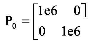
- w is a matrix of parameters to be estimated and is equal to [ ⁇ 0 , ⁇ 0 ] T .
- the estimate w and which is equal to [ ⁇ and 0 , ⁇ and 0 ] T , may be computed recursively using the RLS or Kalman filtering algorithm. Such algorithms are well known to those skilled in the art. Other methods for computing the estimate may be used as well.
- the estimate w and n can be obtained and thus, the pair [ ⁇ and 0 , ⁇ and 0 ] T can be computed.
- the state variables initialization module represented as PLL and NCO initialization module 250 uses the carrier frequency and phase offset estimates obtained from the curve fit algorithm module 240 to initialize the state variables of the PLL 100.
- Figure 3A illustrates the different components of the remove modulation module 220 shown in Figure 2.
- the remove modulation module 220 comprises remove modulation logic 300 configured to communicate with one or more memory elements 301a, 301b and 301c.
- the operation of the remove modulation logic 300 shown in Figure 3A can be readily understood from the flowchart shown in Figure 3B.
- the remove modulation logic 300 estimates, for every received symbol, the angle rotation relative to a previous symbol caused by the channel distortion.
- the memory elements 301a, 301b and 301c are used to hold values of variables such as AccumRotation, FirstTimeFlag and State which are updated and carried from a previous symbol processing interval by the remove modulation logic 300 to a current symbol processing interval.
- the remove modulation logic 300 is illustrated for a Binary Phase Shift Keying (BPSK) modulation implementation, this logic may be implemented for any two-dimensional modulation such as Multiple Phase Shift Keying (MPSK) or Multiple Quadrature Amplitude Modulation (M-QAM).
- MPSK Multiple Phase Shift Keying
- M-QAM Multiple Quadrature Amplitude Modulation
- the remove modulation logic 300 may be applied if the carrier frequency offset f 0 satisfies ⁇ 0 ⁇ 1/(4 T s ) .
- the phase shift from one symbol to another will exceed 90 degrees, which will make the determination as to whether the phase shift is due to the transmitted symbol or the carrier offset difficult.
- the modulation effect may be removed if the carrier frequency offset f 0 satisfies ⁇ 0 ⁇ 1/(2 MT s ) .
- a training sequence known to the receiver may be used to remove the indetermination given ⁇ 0 ⁇ 1/(2 T s ) .
- the flowchart of Figure 3B illustrates the different steps performed by the remove modulation logic 300 in an example implementation.
- a test is performed to determine if this is the first time the module is called (step 305). If the FirstTimeFlag variable is equal to one, the "Yes" branch is taken and the remove modulation module 220 sets the output phase equal to the input phase (step 310).
- the AccumRotation variable and the FirstTimeFlag variable are reset to zero.
- step 330 the input phase value is rotated by adding to its value the value of the AccumRotation variable.
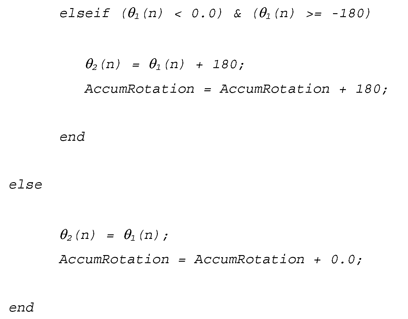
- step 335 the rotated input phase value is confined, if necessary, to the range [-180°, 180°] by using software means, for example, a code written in MATLAB:
- the remove modulation logic 300 ensures that the phase difference, e.g., TempPhase, is confined in the range [-180°, 180°] by using, for example, the above described software means.
- the output phase is calculated at step 350 and the AccumRotation is updated at step 355.
- Step 350 and step 355 may be accomplished using a software means, such as the following MATLAB code:
- the AccumRotation is confined in the range [-180°, 180°] by similar software means to that described above.
- the present state variable is updated at step 360 by setting its value equal to the output phase.
- FIG 4A illustrates the unwrap phase module 230 of Figure 2.
- the unwrap phase module 230 contains an unwrap phase logic 400 whose operation is described by the flowchart shown in Figure 4B.
- the unwrap phase logic 400 performs a modulo operation on the sequence of phase values received from the remove modulation module 220.
- a bounded phase value ⁇ 2 (n) between [-180°, 180°] is converted to its absolute value which allows for a first-order polynomial representation of the sequence of phase values.
- Figure 4B illustrates a flowchart which can be used to implement the unwrap phase logic 400.
- the test step 405 determines if the FirstTimeFlag is equal to one, in which case the "Yes" branch is taken. If the FirstTimeFlag is equal to zero, the unwrap phase logic 400 proceeds along the "No" branch.
- step 410 the output phase is set equal to the input phase and at steps 415 and 420, the AccumRotation and the FirstTimeFlag are reset to zero.
- a rotated phase value is computed by adding to the input phase value the value of AccumRotation.
- a phase difference between the rotated phase value and the present state value is computed.
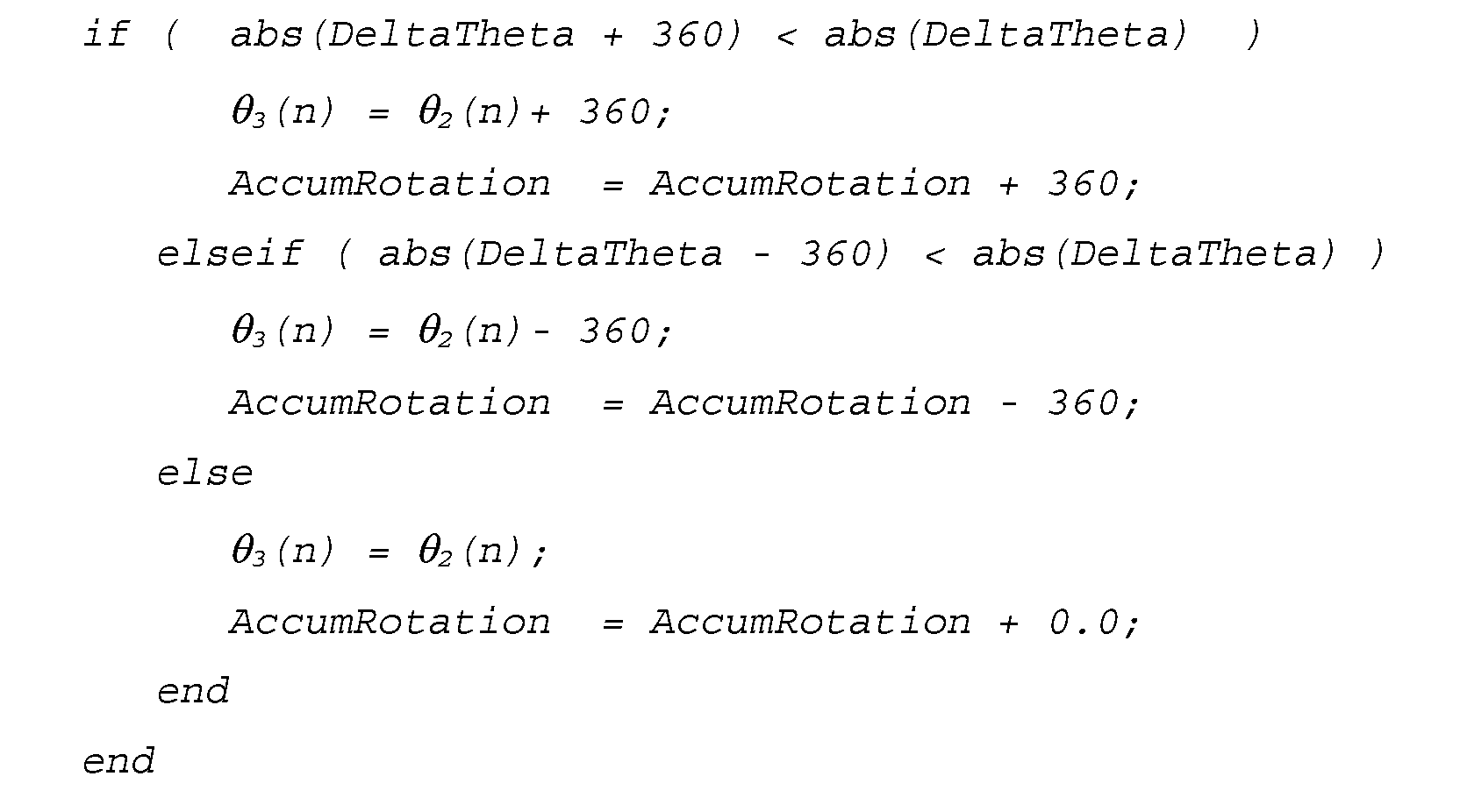
- Step 440 the unwrapped phase value is computed and at step 445 the AccumRotation value is updated.
- Step 440 and step 445 may be implemented using the following exemplary software means written in MATLAB:
- step 450 the present state value is updated and the process ends at step 404.
- Figure 5 shows a table 500 containing phase values generated by different modules of the PLL initialization module 200.
- Table 500 also shows a sequence of transmitted bits (column 502) as well as the transmitted symbols, i.e., "constellation points" (column 504) and the received symbols (column 506).
- Column 508 contains the phase values generated by the phase module 210 of Figure 2.
- Column 510 contains the phase values generated by the remove modulation module 220 of Figure 2.
- Column 512 contains the phase values generated by the unwrap phase module 230 of Figure 2.
- Figure 6 illustrates an exemplary curve obtained by applying the curve fitting algorithm to a sequence of phase values ⁇ 3 (n).
- the noisy phase data represent the input phase values
- the LS and RLS curve-fit represents the straight line approximation of the noisy data
- the LS and RLS predictor is the predicted value obtained by using the RLS method.
- the method of the present invention may be implemented in a number of different ways including software, hardware or a combination thereof. It can be implemented as embedded software in a Digital Signal Processor (DSP) or implemented as an Application Specific Integrated Circuit (ASIC). Other implementation methods may also be used.
- DSP Digital Signal Processor
- ASIC Application Specific Integrated Circuit
Landscapes
- Engineering & Computer Science (AREA)
- Computer Networks & Wireless Communication (AREA)
- Signal Processing (AREA)
- Digital Transmission Methods That Use Modulated Carrier Waves (AREA)
- Stabilization Of Oscillater, Synchronisation, Frequency Synthesizers (AREA)
Abstract
Description

- K0 =[ 0.99900099900100, 0.00000000000000]T
- K1 =[ 0.00000000770834, 0.00277777773493]T
- K2 =[-0.16652789131688, 0.00138865759479]T
- K3 =[-0.19986009717343, 0.00083316678192]T
- K4 =[-0.19988007164837, 0.00055544451064]T
- K5 =[-0.19037646934006, 0.00039674985045]T
- K6 =[-0.17848855883573, 0.00029756592596]T
- K7 =[-0.16659725113632, 0.00023144291728]T
- K8 =[-0.15549681232540, 0.00018515638948]T
- K9 =[-0.14540431489250, 0.00015149312056]T


Claims (16)
- A method for estimating carrier frequency and phase offsets of a digitally modulated signal, comprising:(a) estimating one or more phases of a sequence of digitally modulated symbols;(b) removing from each of the estimated phases an angle rotation introduced by a modulation format, wherein the rotation is determined based on a reference symbol;(c) deriving a set of values from the estimated phases after removal of said angle rotation, wherein said values are a function of the carrier frequency and phase offsets to be estimated; and(d) processing said values to determine estimates of the carrier frequency and phase offsets.
- The method of claim 1 further comprising:(e) initializing the parameters of a Phase-Locked Loop with the estimated carrier frequency and the phase offsets.
- The method of claim 1 or claim 2 wherein step (c) uses an unwrap phase function to derive said set of values.
- The method of claim 1 or claim 2 or claim 3 wherein the processing of step (d) uses an estimation algorithm based on the recursive least-squares method.
- The method of claim 1 or claim 2 or claim 3 wherein the processing of step (d) uses an estimation algorithm based on the Kalman filtering method.
- The method of claim 1 or claim 2 or claim 3 wherein the processing of step (d) uses an estimation algorithm based on the least-mean squares method.
- A method for recovering a carrier phase offset and a carrier frequency offset comprising the steps of:(a) receiving a modulated signal containing a plurality of symbols;(b) determining an angular location of first symbol;(c) determining an angular location of a second symbol;(d) removing the modulation from the second symbol to produce an unmodulated angular sequence; and(e) estimating the carrier phase and frequency offsets by curve fitting the unmodulated angular sequence.
- The method described in claim 7 further comprising the step of:(f) unwrapping the unmodulated angular sequence to compensate for phase discontinuities.
- The method of claim 7 wherein step (f) is based on the recursive least-squares method to perform the curve-fitting.
- The method of claim 7 wherein step (f) is based on the Kalman filtering method to perform the curve-fitting.
- The method of claim 7 wherein step (f) is based on the least-mean squares method to perform the curve-fitting.
- The method of claim 7 wherein the carrier phase offset and the carrier frequency offset are used as initialization parameters in a phase-locked loop.
- An apparatus for estimating a carrier phase offset and a carrier frequency offset, comprising:(a) a phase calculator for estimating phases of a sequence of digitally modulated symbols;(b) a remove modulation module for removing an angle rotation introduced by a modulation format to generate a sequence of phase values representative of the carrier frequency offset and the carrier phase offset; and(c) an estimation module for estimating the carrier frequency offset and the carrier phase offset, whereby the estimation module applies a curve-fitting algorithm to the sequence of phase values to generate a linear function dependent of the carrier frequency offset and the carrier phase offset.
- The apparatus of claim 13 further comprising:(d) an unwrap module for converting the phase estimates generated by the phase calculator module into absolute values.
- The apparatus of claim 13 further coupled to a phase-locked loop to initialize the phase-locked loop with the estimates of the carrier frequency offset and the carrier phase offset.
- The apparatus of claim 13 wherein the estimation module applies a curve-fitting algorithm to the sequence of phase values to estimate the carrier frequency offset and the carrier phase offset.
Applications Claiming Priority (2)
| Application Number | Priority Date | Filing Date | Title |
|---|---|---|---|
| US09/809,748 US6993095B2 (en) | 2001-03-15 | 2001-03-15 | Phase-locked loop initialization via curve-fitting |
| US809748 | 2001-03-15 |
Publications (2)
| Publication Number | Publication Date |
|---|---|
| EP1241846A2 true EP1241846A2 (en) | 2002-09-18 |
| EP1241846A3 EP1241846A3 (en) | 2006-06-07 |
Family
ID=25202130
Family Applications (1)
| Application Number | Title | Priority Date | Filing Date |
|---|---|---|---|
| EP20020100252 Ceased EP1241846A3 (en) | 2001-03-15 | 2002-03-14 | Phase-locked loop initialization via curve-fitting |
Country Status (3)
| Country | Link |
|---|---|
| US (1) | US6993095B2 (en) |
| EP (1) | EP1241846A3 (en) |
| JP (1) | JP3973933B2 (en) |
Cited By (6)
| Publication number | Priority date | Publication date | Assignee | Title |
|---|---|---|---|---|
| GB2376859A (en) * | 2001-02-15 | 2002-12-24 | Central Research Lab Ltd | A method of estimating the carrier frequency of a phase-modulated signal |
| EP1471703A3 (en) * | 2003-04-25 | 2006-08-02 | Nec Corporation | Carrier frequency offset detection and correction |
| EP1349338A3 (en) * | 2002-03-30 | 2006-11-15 | Broadcom Corporation | Compensation of phase and frequency errors in a multicarrier receiver |
| US7903769B2 (en) | 2005-12-12 | 2011-03-08 | Telefonaktiebolaget L M Ericsson (Publ) | Method and apparatus for phase-noise compensation in digital receivers |
| EP2704385A1 (en) * | 2012-08-30 | 2014-03-05 | The Boeing Company | Systems and methods for selection of loop filter bandwidth for carrier phase recovery |
| CN108988932A (en) * | 2018-06-28 | 2018-12-11 | 中国人民解放军63698部队 | Digital tracking receiver emulation platform based on MATLAB |
Families Citing this family (10)
| Publication number | Priority date | Publication date | Assignee | Title |
|---|---|---|---|---|
| KR100807886B1 (en) * | 2001-09-24 | 2008-02-27 | 에스케이 텔레콤주식회사 | Receiver of Orthogonal Frequency Division Multiplexing System |
| AT413282B (en) * | 2002-02-01 | 2006-01-15 | Sandoz Ag | CRYSTALLINE SALTS OF 7 - (((5-AMINO-1,2,4-THIADIAZOL-3-YL) (FLUOROMETHOXY-IMINO) ACETYL) AMINO) -3- ((IMINO-1-PIPERAZINYLMETHYL) |
| US7324612B2 (en) | 2003-02-21 | 2008-01-29 | Conexant, Inc. | Carrier tracking circuit and method including dual numerically controlled oscillators and feedforward phase correction coefficient |
| ATE350847T1 (en) * | 2003-09-05 | 2007-01-15 | Europ Agence Spatiale | METHOD FOR PILOT-ASSISTED CARRIER PHASE SYNCHRONIZATION |
| US7336732B1 (en) * | 2004-07-28 | 2008-02-26 | L-3 Communications Titan Corporation | Carrier frequency detection for signal acquisition |
| US20070016835A1 (en) * | 2005-07-12 | 2007-01-18 | Integrated Device Technology, Inc. | Method and apparatus for parameter adjustment, testing, and configuration |
| TWI376876B (en) * | 2006-10-23 | 2012-11-11 | Realtek Semiconductor Corp | Fraction-n frequency divider and method thereof |
| TWI338456B (en) * | 2006-10-23 | 2011-03-01 | Realtek Semiconductor Corp | Hybrid phase-locked loop |
| US8908809B2 (en) * | 2010-12-15 | 2014-12-09 | At&T Intellectual Property I, L.P. | Complexity reduced feed forward carrier recovery methods for M-QAM modulation formats |
| WO2014132599A1 (en) * | 2013-02-27 | 2014-09-04 | パナソニック株式会社 | Reception apparatus, phase error estimation method, and phase error correction method |
Family Cites Families (10)
| Publication number | Priority date | Publication date | Assignee | Title |
|---|---|---|---|---|
| CA2018855C (en) * | 1989-06-14 | 1993-09-21 | Shousei Yoshida | Burst demodulator for establishing carrier and clock timing from a sequence of alternating symbols |
| US5233632A (en) * | 1991-05-10 | 1993-08-03 | Motorola, Inc. | Communication system receiver apparatus and method for fast carrier acquisition |
| US5287067A (en) * | 1991-10-07 | 1994-02-15 | Nippon Telegraph And Telephone Corporation | Method and apparatus for demodulation with adaptive phase control in quasi-coherent detection |
| JP3148834B2 (en) * | 1995-07-07 | 2001-03-26 | ノーテル・ネットワークス・リミテッド | Method and apparatus for reproducing carrier for digital modulated signal |
| JP3013763B2 (en) * | 1995-08-25 | 2000-02-28 | 日本電気株式会社 | Carrier synchronization unit |
| JP3024524B2 (en) * | 1995-09-25 | 2000-03-21 | 日本電気株式会社 | Carrier synchronization unit and synchronization method |
| US5790570A (en) * | 1996-08-30 | 1998-08-04 | Cornell Research Foundation, Inc. | Concatenated trellis coded modulation and linear block codes |
| US5960044A (en) * | 1996-11-14 | 1999-09-28 | Scientific-Atlanta, Inc. | Apparatus and method for block phase estimation |
| US6421399B1 (en) * | 1998-03-05 | 2002-07-16 | Agere Systems Guardian Corporation | Frequency and phase estimation for MPSK signals |
| US7079574B2 (en) * | 2001-01-17 | 2006-07-18 | Radiant Networks Plc | Carrier phase recovery system for adaptive burst modems and link hopping radio networks |
-
2001
- 2001-03-15 US US09/809,748 patent/US6993095B2/en not_active Expired - Lifetime
-
2002
- 2002-03-14 JP JP2002070010A patent/JP3973933B2/en not_active Expired - Fee Related
- 2002-03-14 EP EP20020100252 patent/EP1241846A3/en not_active Ceased
Cited By (10)
| Publication number | Priority date | Publication date | Assignee | Title |
|---|---|---|---|---|
| GB2376859A (en) * | 2001-02-15 | 2002-12-24 | Central Research Lab Ltd | A method of estimating the carrier frequency of a phase-modulated signal |
| GB2376859B (en) * | 2001-02-15 | 2003-09-24 | Central Research Lab Ltd | A method of estimating the carrier frequency of a phase-modulated signal |
| EP1349338A3 (en) * | 2002-03-30 | 2006-11-15 | Broadcom Corporation | Compensation of phase and frequency errors in a multicarrier receiver |
| US7184506B2 (en) | 2002-03-30 | 2007-02-27 | Broadcom Corporation | Frequency drift and phase error compensation in a VOFDM receiver |
| EP1471703A3 (en) * | 2003-04-25 | 2006-08-02 | Nec Corporation | Carrier frequency offset detection and correction |
| US7496160B2 (en) | 2003-04-25 | 2009-02-24 | Nec Corporation | Frequency offset detection processing system and frequency offset detection processing method using the same |
| US7903769B2 (en) | 2005-12-12 | 2011-03-08 | Telefonaktiebolaget L M Ericsson (Publ) | Method and apparatus for phase-noise compensation in digital receivers |
| EP2704385A1 (en) * | 2012-08-30 | 2014-03-05 | The Boeing Company | Systems and methods for selection of loop filter bandwidth for carrier phase recovery |
| US9042490B2 (en) | 2012-08-30 | 2015-05-26 | The Boeing Company | Systems and methods for carrier phase recovery |
| CN108988932A (en) * | 2018-06-28 | 2018-12-11 | 中国人民解放军63698部队 | Digital tracking receiver emulation platform based on MATLAB |
Also Published As
| Publication number | Publication date |
|---|---|
| JP2002335294A (en) | 2002-11-22 |
| JP3973933B2 (en) | 2007-09-12 |
| US20020176520A1 (en) | 2002-11-28 |
| EP1241846A3 (en) | 2006-06-07 |
| US6993095B2 (en) | 2006-01-31 |
Similar Documents
| Publication | Publication Date | Title |
|---|---|---|
| US6993095B2 (en) | Phase-locked loop initialization via curve-fitting | |
| US6055281A (en) | Passband DQPSK detector for a digital communications receiver | |
| US4959656A (en) | Efficient detection and signal parameter estimation with application to high dynamic GPS receiver | |
| US5233632A (en) | Communication system receiver apparatus and method for fast carrier acquisition | |
| US6212246B1 (en) | Symbol-quality evaluation in a digital communications receiver | |
| EP0551081B1 (en) | Adaptive equalizer and receiver | |
| US6768780B1 (en) | Non-data aided maximum likelihood based feedforward timing synchronization method | |
| US5491724A (en) | Mean phase predictor for maximum a posteriori demodulator | |
| AU621183B2 (en) | A method of rapidly controlling the frequency of a coherent radio receiver and apparatus for carrying out the method | |
| CA2025232C (en) | Carrier recovery system | |
| US5077531A (en) | PSK signal demodulation system | |
| US5940435A (en) | Method for compensating filtering delays in a spread-spectrum receiver | |
| US6650187B1 (en) | Decision directed suppressed carrier symbol-rate PLL with programmable phase discriminator and chip-rate phase extrapolation | |
| JP3778994B2 (en) | Digital communication system | |
| US20110170583A1 (en) | Method for tracking the phase of a signal modulated by continuous phase modulation and synchronization device implementing said method | |
| CN115997371A (en) | frequency offset estimation | |
| US6175600B1 (en) | System for detecting the presence of a digital signal carrier wave, and a receiver including such a system | |
| JPH09219732A (en) | Lock detector for data synchronizer and operating method thereof | |
| JP4315549B2 (en) | Signal carrier recovery processing method | |
| US5774508A (en) | Data synchronizer phase detector and method of operation thereof | |
| KR100310294B1 (en) | Recovery apparatus of decision-directed darrier | |
| EP1060601B1 (en) | Demodulator having rotation means for frequency offset correction | |
| US6859507B2 (en) | Method and apparatus for correcting a signal | |
| CA2110032C (en) | Frequency error detecting device capable of correctly detecting a frequency error between a carrier frequency and a standard frequency | |
| KR100325690B1 (en) | Apparatus and Method of Decision-Directed Carrier Recovery Based On LMS Method |
Legal Events
| Date | Code | Title | Description |
|---|---|---|---|
| PUAI | Public reference made under article 153(3) epc to a published international application that has entered the european phase |
Free format text: ORIGINAL CODE: 0009012 |
|
| AK | Designated contracting states |
Kind code of ref document: A2 Designated state(s): AT BE CH CY DE DK ES FI FR GB GR IE IT LI LU MC NL PT SE TR |
|
| AX | Request for extension of the european patent |
Free format text: AL;LT;LV;MK;RO;SI |
|
| PUAL | Search report despatched |
Free format text: ORIGINAL CODE: 0009013 |
|
| AK | Designated contracting states |
Kind code of ref document: A3 Designated state(s): AT BE CH CY DE DK ES FI FR GB GR IE IT LI LU MC NL PT SE TR |
|
| AX | Request for extension of the european patent |
Extension state: AL LT LV MK RO SI |
|
| 17P | Request for examination filed |
Effective date: 20061206 |
|
| AKX | Designation fees paid |
Designated state(s): DE FR GB |
|
| 17Q | First examination report despatched |
Effective date: 20071122 |
|
| STAA | Information on the status of an ep patent application or granted ep patent |
Free format text: STATUS: THE APPLICATION HAS BEEN REFUSED |
|
| 18R | Application refused |
Effective date: 20150504 |