EP1240512B1 - Permeation layer attachment chemistry and method - Google Patents
Permeation layer attachment chemistry and method Download PDFInfo
- Publication number
- EP1240512B1 EP1240512B1 EP00992315A EP00992315A EP1240512B1 EP 1240512 B1 EP1240512 B1 EP 1240512B1 EP 00992315 A EP00992315 A EP 00992315A EP 00992315 A EP00992315 A EP 00992315A EP 1240512 B1 EP1240512 B1 EP 1240512B1
- Authority
- EP
- European Patent Office
- Prior art keywords
- electrode
- permeation layer
- linker molecule
- permeation
- layer material
- Prior art date
- Legal status (The legal status is an assumption and is not a legal conclusion. Google has not performed a legal analysis and makes no representation as to the accuracy of the status listed.)
- Expired - Lifetime
Links
Images






Classifications
-
- G—PHYSICS
- G01—MEASURING; TESTING
- G01N—INVESTIGATING OR ANALYSING MATERIALS BY DETERMINING THEIR CHEMICAL OR PHYSICAL PROPERTIES
- G01N33/00—Investigating or analysing materials by specific methods not covered by groups G01N1/00 - G01N31/00
- G01N33/48—Biological material, e.g. blood, urine; Haemocytometers
-
- G—PHYSICS
- G01—MEASURING; TESTING
- G01N—INVESTIGATING OR ANALYSING MATERIALS BY DETERMINING THEIR CHEMICAL OR PHYSICAL PROPERTIES
- G01N27/00—Investigating or analysing materials by the use of electric, electrochemical, or magnetic means
- G01N27/26—Investigating or analysing materials by the use of electric, electrochemical, or magnetic means by investigating electrochemical variables; by using electrolysis or electrophoresis
- G01N27/28—Electrolytic cell components
- G01N27/40—Semi-permeable membranes or partitions
-
- G—PHYSICS
- G01—MEASURING; TESTING
- G01N—INVESTIGATING OR ANALYSING MATERIALS BY DETERMINING THEIR CHEMICAL OR PHYSICAL PROPERTIES
- G01N33/00—Investigating or analysing materials by specific methods not covered by groups G01N1/00 - G01N31/00
- G01N33/48—Biological material, e.g. blood, urine; Haemocytometers
- G01N33/50—Chemical analysis of biological material, e.g. blood, urine; Testing involving biospecific ligand binding methods; Immunological testing
- G01N33/53—Immunoassay; Biospecific binding assay; Materials therefor
- G01N33/543—Immunoassay; Biospecific binding assay; Materials therefor with an insoluble carrier for immobilising immunochemicals
- G01N33/54366—Apparatus specially adapted for solid-phase testing
- G01N33/54373—Apparatus specially adapted for solid-phase testing involving physiochemical end-point determination, e.g. wave-guides, FETS, gratings
- G01N33/5438—Electrodes
-
- B—PERFORMING OPERATIONS; TRANSPORTING
- B01—PHYSICAL OR CHEMICAL PROCESSES OR APPARATUS IN GENERAL
- B01J—CHEMICAL OR PHYSICAL PROCESSES, e.g. CATALYSIS OR COLLOID CHEMISTRY; THEIR RELEVANT APPARATUS
- B01J2219/00—Chemical, physical or physico-chemical processes in general; Their relevant apparatus
- B01J2219/00274—Sequential or parallel reactions; Apparatus and devices for combinatorial chemistry or for making arrays; Chemical library technology
- B01J2219/00583—Features relative to the processes being carried out
- B01J2219/00603—Making arrays on substantially continuous surfaces
- B01J2219/00653—Making arrays on substantially continuous surfaces the compounds being bound to electrodes embedded in or on the solid supports
-
- B—PERFORMING OPERATIONS; TRANSPORTING
- B01—PHYSICAL OR CHEMICAL PROCESSES OR APPARATUS IN GENERAL
- B01J—CHEMICAL OR PHYSICAL PROCESSES, e.g. CATALYSIS OR COLLOID CHEMISTRY; THEIR RELEVANT APPARATUS
- B01J2219/00—Chemical, physical or physico-chemical processes in general; Their relevant apparatus
- B01J2219/00274—Sequential or parallel reactions; Apparatus and devices for combinatorial chemistry or for making arrays; Chemical library technology
- B01J2219/00583—Features relative to the processes being carried out
- B01J2219/00603—Making arrays on substantially continuous surfaces
- B01J2219/00659—Two-dimensional arrays
-
- B—PERFORMING OPERATIONS; TRANSPORTING
- B01—PHYSICAL OR CHEMICAL PROCESSES OR APPARATUS IN GENERAL
- B01J—CHEMICAL OR PHYSICAL PROCESSES, e.g. CATALYSIS OR COLLOID CHEMISTRY; THEIR RELEVANT APPARATUS
- B01J2219/00—Chemical, physical or physico-chemical processes in general; Their relevant apparatus
- B01J2219/00274—Sequential or parallel reactions; Apparatus and devices for combinatorial chemistry or for making arrays; Chemical library technology
- B01J2219/00718—Type of compounds synthesised
- B01J2219/0072—Organic compounds
- B01J2219/00722—Nucleotides
-
- B—PERFORMING OPERATIONS; TRANSPORTING
- B01—PHYSICAL OR CHEMICAL PROCESSES OR APPARATUS IN GENERAL
- B01J—CHEMICAL OR PHYSICAL PROCESSES, e.g. CATALYSIS OR COLLOID CHEMISTRY; THEIR RELEVANT APPARATUS
- B01J2219/00—Chemical, physical or physico-chemical processes in general; Their relevant apparatus
- B01J2219/00274—Sequential or parallel reactions; Apparatus and devices for combinatorial chemistry or for making arrays; Chemical library technology
- B01J2219/00718—Type of compounds synthesised
- B01J2219/0072—Organic compounds
- B01J2219/00725—Peptides
-
- C—CHEMISTRY; METALLURGY
- C40—COMBINATORIAL TECHNOLOGY
- C40B—COMBINATORIAL CHEMISTRY; LIBRARIES, e.g. CHEMICAL LIBRARIES
- C40B40/00—Libraries per se, e.g. arrays, mixtures
- C40B40/04—Libraries containing only organic compounds
- C40B40/06—Libraries containing nucleotides or polynucleotides, or derivatives thereof
-
- C—CHEMISTRY; METALLURGY
- C40—COMBINATORIAL TECHNOLOGY
- C40B—COMBINATORIAL CHEMISTRY; LIBRARIES, e.g. CHEMICAL LIBRARIES
- C40B40/00—Libraries per se, e.g. arrays, mixtures
- C40B40/04—Libraries containing only organic compounds
- C40B40/10—Libraries containing peptides or polypeptides, or derivatives thereof
Definitions
- This invention relates to the attachment of a layer of polymeric material to a substrate surface. More particularly, this invention relates to chemistries and methods for covalently attaching a porous polymeric material to an electrically conductive substrate, such as a metal electrode of a microchip circuit.
- the microchips In the art of electronically addressable microchips that are used to direct biomaterials, such as nucleic acids and proteins, from one point in a solution to another, the microchips should be designed so that electric potential from the microchip electrodes will translate to the solution overlying the microchip such that any electrochemistry occurring from the electrode surface will neither damage the electrodes themselves, nor any biomaterials in the solution. Generally, protection from such damage is provided by the use of a porous membrane layer deposited over the microchip electrodes. Usually, such layer comprises materials derived from natural or synthetic polymers such as agarose or polyacrylamide, respectively. These types of materials allow electrochemical products generated at the electrode surface to travel through their porous matrix or 'permeation layer' and into the solution immediately above the electrodes.
- Microdelamination involves the electrochemical degradation of the chemical interface between the permeation layer and the electrode itself. It is observed by the formation of raised bulges in the permeation layer, or by ringlets visible due to defraction of light from the delaminated layer when appropriately viewed by a confocal microscope and results in the loss of consistency in permeation layer performance (possibly due to the loss of control over the electric field uniformity). Macrodelamination, on the other hand, is caused by a mismatch of the surface energies between the permeation layer and the chip substrate and results in permeation layer peeling (lift-off) which can extend across the entire microchip surface. Since the permeation layer provides a means for chemical anchorage of analytes present in the liquid overlay, its physical loss by macrodelamination results in catastrophic chip failure during bioassays.
- the invention described in this Letters Patent uses a relationship between electric current and voltage wherein electric current densities are at least 0.04 nA/ ⁇ m 2 and/or voltage drops are between 1 and 3 V.
- the electric current density is defined as the electric current divided by the area of the electrode used to support it.
- the effectiveness of the translocation of charged biomolecules such as nucleotide oligomers within an electronically-driven system such as that described herein depends on the generation of the proper gradient of positively and negatively charged electrochemical species by the anode and cathode, respectively.
- effective nucleic acid i.e. either DNA or RNA
- transport may be accomplished by generation of protons and hydroxyl anions when the potential at the anode is greater than +1.29 V with respect to a 'saturated calomel electrode' (SCE).
- SCE 'saturated calomel electrode'
- noncovalently-attached permeation layers prove to be unsatisfactory since such systems are likely to experience micro- and sometimes macrodelamination.
- the transport efficiency of charged molecules increases with increasing current density, thus driving the desire for operation at higher voltage drops and current densities and, thus, the need for evermore robust permeation layers.
- the current invention provides a unique system for the covalent attachment of a porous 'permeation layer' to the surface of electronically addressable microchips.
- the covalent attachment is between chemical moieties of the permeation layer and metal/silicide, metal/metal, or organic electrodes.
- Preferred metal/silicide electrodes include platinum silicide (PtSi), tungsten silicide (WTi), titanium silicide (TiSi), and gold silicide (AuSi).
- Preferred metal/metal electrodes include platinum/titanium (PtTi) and gold/titanium (AuTi).
- Preferred organic electrodes include materials such as poly(phenylene vinylene), polythiophene, and polyaniline.
- the covalent attachment comprises a linking moiety that provides an attachment mechanism for bonding the linker to the silanol moiety of a metal/Si surface and a separate moiety for bonding the linker to the permeation layer.
- the attachment mechanism of the linker to the electrode is the same in that the moiety of the linker attaching to the electrode will react with specific metals and reactive centers on organic molecules to form covalent bonds.
- Another embodiment of the present invention provides a method of covalently attaching a permeation layer having reactive moieties to a metal/silicide, metal/metal, or an organic electrode of an electronically addressable microchip comprising:
- these linkage groups which contain a silicide group can react with hydroxyl groups bonded to an oxygen moiety of the electrode surface.
- the X moiety comprises chemical groups that are available to covalently react with reactive centers of the permeation layer polymer.
- the permeation layer is a material suitable for transmitting electronic charge from an electrode to a solution overlaying the electrode.
- Materials contemplated for constructing polymers used for the permeation layer may include, agarose and glyoxylagarose. Also disclosed are acrylamide, methacrylamide, polyacrylamide, materials made from other synthetic monomers, and porous inorganic oxides created through a sol-gel process ( Brinker et al., Sol-Gel Science, Academic Press, San Diego, 1990 ).
- synthetic monomers used to make polymeric permeation layers may include those selected from the group consisting of epoxides, alkenyl moieties including, but not limited to, substituted or unsubstituted ⁇ , ⁇ unsaturated carbonyls wherein the double bond is directly attached to a carbon which is double bonded to an oxygen and single bonded to another oxygen, nitrogen, sulfur, halogen, or carbon; vinyl, wherein the double bond is singly bonded to an oxygen, nitrogen; halogen, phosphorus or sulfur; allyl, wherein the double bond is singly bonded to a carbon which is bonded to an oxygen, nitrogen, halogen, phosphorus or sulfur; homoallyl, wherein the double bond is singly bonded to a carbon which is singly bonded to another carbon which is then singly bonded to an oxygen, nitrogen, halogen, phosphorus or sulfur; and alkynyl moieties wherein a triple bond exists between two carbon atoms.
- the covalently attached permeation layer is kept from delaminating while the anode is charged with an electronic potential above +1.29V/SCE and/or the cathode with a potential below -0.89 V/SCE.
- the current flow between the electrodes has a density sufficient to induce the transport of molecules in the solution above the electrodes of the microchip. Such density is preferably between 0.04 and 1 nA/ ⁇ m 2 .
- the transported molecules In the art of electronically addressable microchips used for transporting charged molecules from one point in a solution to another, the transported molecules must be protected from direct contact with the electrodes of the microchip and ions produced at the electrode when the electrodes are biased to impart an electric field to the solution. Protection is provided by an insulating membrane, i.e., the permeation layer, which also allows for the flow of charge from the electrode to the solution without damaging the transported molecules.
- the insulating membrane is a polymeric material such as agarose or cross-linked polyacrylamide. These materials are ideal in that they are porous and allow electrochemical products created at the electrode to escape to the overlying solution.
- such insulating membrane materials can comprise, but are not limited to, agarose and glyoxylagarose. Also described herein are acrylamide, methacrylamide, polyacrylamide, materials made from other synthetic monomers, and porous inorganic oxides created through a sol-gel process.
- synthetic monomers used to make polymeric permeation layers may include those selected from the group consisting of epoxides, alkenyl moieties including, but not limited to, substituted or unsubstituted ⁇ , ⁇ unsaturated carbonyls wherein the double bond is directly attached to a carbon which is double bonded to an oxygen and single bonded to another oxygen, nitrogen, sulfur, halogen, or carbon; vinyl, wherein the double bond is singly bonded to an oxygen, nitrogen, halogen, phosphorus or sulfur; allyl, wherein the double bond is singly bonded to a carbon which is bonded to an oxygen, nitrogen, halogen, phosphorus or sulfur; homoallyl, wherein the double bond is singly bonded to a carbon which is singly bonded to another carbon which is then singly bonded to an oxygen, nitrogen, halogen, phosphorus or sulfur; and alkynyl moieties wherein a triple bond exists between two carbon atoms.
- the porous insulating layer or permeation layer may be linked to the electrode by a linking moiety that has at least two reactive centers.
- Linkers having suitable characteristics such as that shown in Fig. 1 are provided in Table I, wherein only APS and AEAPS belong to the present invention.
- FIG. 2 shows a schematic of one embodiment wherein AEAPS is used to bond the electrode to the permeation layer.
- the PtSi electrode microchip is first treated with an argon plasma for 5 minutes at 250 mTorr and 250 Watts.
- the chip is then treated with AEAPS by vapor deposition over 5 minutes at room temperature then cured onto the chip by heating for 2 hours at 90°C. This causes the linker to covalently bind to the hydroxyl groups of the silicide moiety in the PtSi electrode.
- the permeation polymer for example glyoxylagarose
- the permeation polymer for example glyoxylagarose
- NaBH 3 CN NaBH 3 CN
- a UV-initiated free radical polymerization reaction can be conducted between the monomers which will make up the permeation layer and the vinyl moieties present at the surface of MOTS- or AMPTS linker-derived electrodes, thereby synthesizing the permeation layer and covalently anchoring it to the electrode in a single step.
- Agarose permeation layer matrix was attached to a PtSi electrode microchip following deposition of either APS or AEAPS by one of two methodologies.
- APS and AEAPS were deposited by exposure of the chip to a 0.1 wt % silane/dry MeOH solution for 1 hour at room temperature. The chips were rinsed in EtOH and cured at 90°C for 1 hour. In parallel experiments, APS and AEAPS linkers were deposited onto microchips by a vapor of neat silane in humid atmosphere for 5 min. at room temperature followed by a two hour cure at 90°C.
- the microchips were subjected to electronic assays wherein the electrodes were biased with three direct current (DC) impulses for 2 minutes each at 200, 500, 700, and 1000 nAmps/ 80 ⁇ m pad (i.e., 0.04, 0.10, 0.14 and 0.20 nA/ ⁇ m 2 ) using a model 236 Source-Measure unit (Keithley Instruments Inc., Cleveland, OH). Following the set of three DC impulses, the electrodes were biased with a sequence of 150 negative pulses, each comprised of a 0.1 sec. ON state at -0.2 nA/ ⁇ m 2 , followed by a 0.2 sec. OFF state at 0 nA/ ⁇ m 2 .
- DC direct current
- the attachment schemes using vapor deposition of the linkers provided protection from delamination up to DC impulses of 700 nA for an 80 ⁇ m electrode (0.14 nA/ ⁇ m 2 ).
- Table II samp 200 nA 200 nA 200 nA -luA 500 nA 500 nA 500 nA -luA 700 nA 700 nA DC1 DC2 DC3 AC DC1 DC2 DC3 AC DC1 DC2 A PtSi (no permlayer) + + + + + + + + + + + + + + + + + + + + + + + + + + + + + + + + + + + + + + + + + + + + + + + + + + + + + + + + + + + + + + + + + + + + + + + + + + + + + + + + + + + + + + + + + + + + + + + + + + + + + + + + + + + + + + + + + + + + + + + + + + + + + + + +
- delamination will occur at low levels of DC (200 nA (0.04 nA/ ⁇ m 2 ) after second DC pulse) where no covalent linker attachment is used to anneal the permeation layer to the electrode (Figs. 3A and B ).
- DC 200 nA (0.04 nA/ ⁇ m 2 ) after second DC pulse
- the delamination does not appear until the electrode has been exposed to the second DC pulse at 700 nA (0.14 nA/ ⁇ m 2 ) (delamination extended to 25% of the pad area at 3 min. past shut-off) with complete delamination by 2 minutes past third DC shut-off (Figs. 4A-D ).
- delamination of the permeation layer from the electrode was tested using a multilayer permeation layer wherein the layers were applied using spin coating techniques then reacted to cause the linking moieties to covalently bond the layers together and to the electrode.
- microchips having PtSi electrodes were cleaned with oxygen plasma for 10 minutes followed by argon plasma for 10 minutes.
- AEAPS was then vapor-deposited for 5 minutes followed by curing at 90°C under vacuum.
- a first layer solution comprising 2.5% glyoxylagarose solution (NuFix) which had been stirred for 10 minutes at room temperature then boiled 7 minutes followed by filtering at 1.2 ⁇ m into the ASC device reservoir at 65°C, was spin-deposited onto the microchips with an automatic spin-coating device (ASC).
- ASC automatic spin-coating device
- a second layer comprising streptavidin (Scripps) at 5 mg/ml in 10 mM sodium phosphate, 250 mM NaCl (pH 7.2) which was filtered at 0.2 ⁇ m into the ASC reservoir and maintained at room temperature, was deposited similarly.
- the bottom layer was spin-coated at either 1500 or 2500 rpm, while the top layer was spin-coated at 5,000 rpm.
- the reaction for the reduction of the Schiff bases generated between streptavidin and glyoxylagarose, and between the AEAPS surface and glyoxylagarose was carried out by treating the coated microchip with 0.2 M NaBH 3 CN 0.1 M sodium phosphate (pH 7.4) for 1 hr.
- Table III the thickness of the double permeation layer was examined where the substrate contained either plain platinum electrodes or PtSi electrodes using two different rotational speeds for the bottom layer deposition. The results indicate that spin-coating results in deposition of permeation layers of variable thicknesses.
- Table III Microchip type Bottom layer spun at 1.5K rpm, bilayer thickness in nanometers Bottom layer spun at 2.5K rpm, bilayer thickness in nanometers Pt/AEAPS/agarose 587 ⁇ 4 465 ⁇ 4 668 ⁇ 4 465 ⁇ 4 668 ⁇ 3 --- PtSi/AEAPS/agarose 744 ⁇ 17 511 ⁇ 4 685 ⁇ 1 620 ⁇ 5 494 ⁇ 90
- the chips as fabricated in this example were tested for resistance to delamination.
- 9 electrode pads were individually addressed from two separate chips in 50 mM fresh Histidine buffer. These pads showed consistent delamination past the second two-minute direct current pulse of 500 nA/ 80 ⁇ m pad (0.1 nA/ ⁇ m 2 ) (Fig. 5A ).
- 6 pads were individually addressed from 2 of the PtSi microchips under the same conditions. These PtSi pads had no delamination up to several ⁇ A/pad (Fig. 5B ).
- the PtSi electrode using the AEAPS attachment linker provided protection from delamination.
- protocol A the microchips were biased at +800 nA/pad (0.16 nA/ ⁇ m 2 ) for 38 milliseconds (ms), -800 nA/pad for 25 ms, cycled for a total of 25 seconds using 3 pads each pulse.
- protocol B the microchips were biased at +1.6 ⁇ A/pad (0.32 nA/ ⁇ m 2 ) for 19 ms, -1.6 ⁇ A/pad for 12 ms, and cycled for a total of 14 seconds each on 3 pads addressed simultaneously. Images were taken using an INM 100 confocal microscope (Leica).
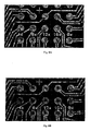
- Figure 6A shows Pt chips that were biased using protocol A, followed by 0, 4, 8, 12 or 16 repeats of protocol B.
- the images show that delamination begins after 8 repeats of protocol B.
- the PtSi chips (Fig. 6B ) showed delamination to a much less extent at the 8 th biasing.
- the chips were assayed with smaller stringency increments using biasing repeats of 2, 4, 6, and 8 times.
- delamination began to occur at bias repeat number 6 (Fig. 7A ).
- the PtSi chip showed less delamination effect at the same level of electrodynamic stress (Fig. 7B ).
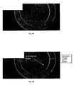
- methacryloylsilanes are employed as linkers for attaching synthetic permeation layers such as acrylamide-based hydrogels to Pt and PtSi chips. Additionally, the integrity of the permeation layer was examined using a technique wherein glass beads are applied to the surface of the permeation layer as a reference upon which the confocal microscope can focus. This enables permeation layer thickness determination and facilitates the monitoring of permeation layer distortions due to such things as delamination.
- Figure 8 shows a Pt microchip having an agarose permeation layer wherein the thickness of the layer before electronic biasing was determined to be 3.0 ⁇ 0.5 ⁇ m.
- the figure shows the focal point at the position of the beads above the electrode.
- the underlying electrode is slightly out of focus.
- Figure 9 the same electrode during a bias at +200 nA (0.04 nA/ ⁇ m 2 ) with direct current without observable distortion of the permeation layer.
- the beads migrate to the electrode due to the positive bias. Following this two-minute bias, the impulse was terminated and the electrode observed for changes in its appearance.
- the beads resting over the center of the electrode moved to a location 4.0 ⁇ 0.5 ⁇ m above the electrode based on the vertical shift required to bring said beads back into the focal plane.
- the permeation layer underwent a 1 ⁇ m expansion.
- this expansion appears to be related to the delamination of the permeation layer from the electrode (microdelamination) as indicated by the presence of concentric rings visible at the edges of the electrode pad. Additionally, in other experiments, not shown, we have observed permeation layer thickness distortions from 2 to 6 ⁇ m occurring with delamination.
- acrylamide-based hydrogel permeation layers anchored to PtSi electrodes via the MOTS linker were exposed to a +200 nA (0.04 nA/ ⁇ m 2 ) bias for 2 minutes and examined for delamination.
- Fig. 12 shows beads resting atop the permeation layer 6 ⁇ m above the electrode surface. The beads remained at the same position above the electrode after bias shut-off, indicating that no distortion of the permeation layer occurred.
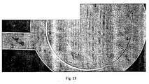
- Fig. 13 shows the same pad with the focal point positioned at the electrode. No delamination ringlets were observed.
- Table IV chip type bias conditions dry thickness initial wet thickness post address distortion integrity of electrode/ permeation layer bond Pt/agarose 200nA, 2 min (0.04 nA/ ⁇ m 2 ) 0.80 ⁇ 0.01 3.0 ⁇ 0.5 4.0 ⁇ 0.5 delamination & distortion 200nA, 2 min (0.04 nA/ ⁇ m 2 ) 0.80 ⁇ 0.01 3.0 ⁇ 0.5 6.0 ⁇ 0.5 delamination & distortion Pt/polyacrylamide 200nA, 2 min (0.04 nA/ ⁇ m 2 ) 2.0 ⁇ 0.1 5.0 ⁇ 0.5 9.0 ⁇ 0.5 delamination & distortion 200nA, 2 min (0.04 nA/ ⁇ m 2 ) 1.9 ⁇ 0.1 5.0 ⁇ 0.5 9.0 ⁇ 0.5 delamination & distortion PtSi/polyacrylamide 200nA, 2 min (0.04 nA/ ⁇ m 2 ) 2.0 ⁇ 0.1 5.0 ⁇ 0.5 5.0 ⁇ 0.5 intact 500nA, 1 min (0.1 nA/ ⁇ m 2 ) 2.0 ⁇ 0.1 6.0 ⁇ 0.5 6.0 ⁇ 0.5 intact
Landscapes
- Health & Medical Sciences (AREA)
- Life Sciences & Earth Sciences (AREA)
- Immunology (AREA)
- Chemical & Material Sciences (AREA)
- Engineering & Computer Science (AREA)
- Molecular Biology (AREA)
- Biomedical Technology (AREA)
- Hematology (AREA)
- Biochemistry (AREA)
- General Health & Medical Sciences (AREA)
- General Physics & Mathematics (AREA)
- Physics & Mathematics (AREA)
- Pathology (AREA)
- Urology & Nephrology (AREA)
- Analytical Chemistry (AREA)
- Food Science & Technology (AREA)
- Medicinal Chemistry (AREA)
- Microbiology (AREA)
- Biotechnology (AREA)
- Electrochemistry (AREA)
- Chemical Kinetics & Catalysis (AREA)
- Cell Biology (AREA)
- Investigating Or Analyzing Materials By The Use Of Electric Means (AREA)
- Physical Or Chemical Processes And Apparatus (AREA)
- Immobilizing And Processing Of Enzymes And Microorganisms (AREA)
- Laminated Bodies (AREA)
- Separation Using Semi-Permeable Membranes (AREA)
- Measuring Or Testing Involving Enzymes Or Micro-Organisms (AREA)
Abstract
Description
- This invention relates to the attachment of a layer of polymeric material to a substrate surface. More particularly, this invention relates to chemistries and methods for covalently attaching a porous polymeric material to an electrically conductive substrate, such as a metal electrode of a microchip circuit.
- The following description provides a summary of information relevant to the present invention. It is not an admission that any of the information provided herein is prior art to the presently claimed invention, nor that any of the publications specifically or implicitly referenced are prior art to the invention.
- In the art of electronically addressable microchips that are used to direct biomaterials, such as nucleic acids and proteins, from one point in a solution to another, the microchips should be designed so that electric potential from the microchip electrodes will translate to the solution overlying the microchip such that any electrochemistry occurring from the electrode surface will neither damage the electrodes themselves, nor any biomaterials in the solution. Generally, protection from such damage is provided by the use of a porous membrane layer deposited over the microchip electrodes. Usually, such layer comprises materials derived from natural or synthetic polymers such as agarose or polyacrylamide, respectively. These types of materials allow electrochemical products generated at the electrode surface to travel through their porous matrix or 'permeation layer' and into the solution immediately above the electrodes.
- Although materials such as those noted above have been found useful in the role of a porous membrane having desired qualities, it has been found that because of the methodologies commonly used to layer such membranes onto the microchip substrate, the membranes are prone to separate or 'delaminate' from the electrode surface. It is believed this delamination is caused by a change in the chemical make-up at the interface between the permeation layer and the electrode resulting from the application of electronic potential at the electrode and by physical disruption from charged ions and gases emanating from the electrode. Such delamination can be viewed from the standpoint of 'microdelamination' and 'macrodelamination'.
- Microdelamination involves the electrochemical degradation of the chemical interface between the permeation layer and the electrode itself. It is observed by the formation of raised bulges in the permeation layer, or by ringlets visible due to defraction of light from the delaminated layer when appropriately viewed by a confocal microscope and results in the loss of consistency in permeation layer performance (possibly due to the loss of control over the electric field uniformity). Macrodelamination, on the other hand, is caused by a mismatch of the surface energies between the permeation layer and the chip substrate and results in permeation layer peeling (lift-off) which can extend across the entire microchip surface. Since the permeation layer provides a means for chemical anchorage of analytes present in the liquid overlay, its physical loss by macrodelamination results in catastrophic chip failure during bioassays.
- Electronically addressable systems such as the microchips considered herein follow Ohm's law which establishes the relationship between the voltage drop (V) between two electrodes (i.e., the anode, placed at a positive potential and the other, the cathode, placed at a negative potential), and the electric current (I) which flows between these electrodes, as follows:

where R is the electrical resistance of the medium between the anode and the cathode. In systems where a permeation layer is present over such electrodes, the value of R is greatly determined by the physical and chemical nature of said permeation layer. Thus, according to formula (1), the difference between the electronic potentials applied to the electrodes is directly proportional to the intensity or density of the electric current which flows through them. The invention described in this Letters Patent uses a relationship between electric current and voltage wherein electric current densities are at least 0.04 nA/µm2 and/or voltage drops are between 1 and 3 V. The electric current density is defined as the electric current divided by the area of the electrode used to support it. - Additionally, the effectiveness of the translocation of charged biomolecules such as nucleotide oligomers within an electronically-driven system such as that described herein depends on the generation of the proper gradient of positively and negatively charged electrochemical species by the anode and cathode, respectively. For example, effective nucleic acid (i.e. either DNA or RNA) transport may be accomplished by generation of protons and hydroxyl anions when the potential at the anode is greater than +1.29 V with respect to a 'saturated calomel electrode' (SCE). When subjected to such demanding operating conditions, noncovalently-attached permeation layers prove to be unsatisfactory since such systems are likely to experience micro- and sometimes macrodelamination. Moreover, the transport efficiency of charged molecules increases with increasing current density, thus driving the desire for operation at higher voltage drops and current densities and, thus, the need for evermore robust permeation layers.
- Therefore, a need still remains for methodologies for keeping permeation layers from delaminating from electronic microchip substrates and particularly from the electrode pads themselves. We have discovered an improvement in permeation layer attachment chemistry that provides a significant increase in permeation layer performance. Specifically, we have solved the problem of micro- and macrodelamination by discovery of a covalent chemistry linkage system that, as applied to electronically addressable microchip art, can be incorporated between the microchip and the permeation layer matrix. This chemistry is applicable to a variety of permeation layer compositions, including polymers, hydrogels, glyoxylagarose, and is able to withstand current densities of at least 0.04 nA/µm2 and/or voltage drops between 1 and 3 V.
- The current invention provides a unique system for the covalent attachment of a porous 'permeation layer' to the surface of electronically addressable microchips. In a preferred embodiment, the covalent attachment is between chemical moieties of the permeation layer and metal/silicide, metal/metal, or organic electrodes. Preferred metal/silicide electrodes include platinum silicide (PtSi), tungsten silicide (WTi), titanium silicide (TiSi), and gold silicide (AuSi). Preferred metal/metal electrodes include platinum/titanium (PtTi) and gold/titanium (AuTi). Preferred organic electrodes include materials such as poly(phenylene vinylene), polythiophene, and polyaniline.
- In an example of this embodiment, the covalent attachment comprises a linking moiety that provides an attachment mechanism for bonding the linker to the silanol moiety of a metal/Si surface and a separate moiety for bonding the linker to the permeation layer. Where metal/metal and organic electrodes are employed, the attachment mechanism of the linker to the electrode is the same in that the moiety of the linker attaching to the electrode will react with specific metals and reactive centers on organic molecules to form covalent bonds.
- Another embodiment of the present invention provides a method of covalently attaching a permeation layer having reactive moieties to a metal/silicide, metal/metal, or an organic electrode of an electronically addressable microchip comprising:
- a) contacting the surface of the electrode with a linker molecule by vapor deposition wherein the linker molecule comprises a first reactive moiety which is capable of reacting with the electrode surface to form a covalent bond with the electrode material, and a second reactive moiety which is capable of reacting with a permeation layer material;
- b) reacting the first reactive moiety of the linker molecule with the electrode surface to form a covalent bond between the linker molecule and the electrode surface;
- c) synthesizing the permeation layer by reacting the second reactive moiety of the linker molecule with the permeation layer material;
- In the example of the metal/Si electrodes, these linkage groups, which contain a silicide group can react with hydroxyl groups bonded to an oxygen moiety of the electrode surface. On the other end of the linker, the X moiety comprises chemical groups that are available to covalently react with reactive centers of the permeation layer polymer.
- In another embodiment, the permeation layer is a material suitable for transmitting electronic charge from an electrode to a solution overlaying the electrode. Materials contemplated for constructing polymers used for the permeation layer may include, agarose and glyoxylagarose. Also disclosed are acrylamide, methacrylamide, polyacrylamide, materials made from other synthetic monomers, and porous inorganic oxides created through a sol-gel process (Brinker et al., Sol-Gel Science, Academic Press, San Diego, 1990). It is also described herein that synthetic monomers used to make polymeric permeation layers may include those selected from the group consisting of epoxides, alkenyl moieties including, but not limited to, substituted or unsubstituted α, β unsaturated carbonyls wherein the double bond is directly attached to a carbon which is double bonded to an oxygen and single bonded to another oxygen, nitrogen, sulfur, halogen, or carbon; vinyl, wherein the double bond is singly bonded to an oxygen, nitrogen; halogen, phosphorus or sulfur; allyl, wherein the double bond is singly bonded to a carbon which is bonded to an oxygen, nitrogen, halogen, phosphorus or sulfur; homoallyl, wherein the double bond is singly bonded to a carbon which is singly bonded to another carbon which is then singly bonded to an oxygen, nitrogen, halogen, phosphorus or sulfur; and alkynyl moieties wherein a triple bond exists between two carbon atoms.
- In another embodiment, the covalently attached permeation layer is kept from delaminating while the anode is charged with an electronic potential above +1.29V/SCE and/or the cathode with a potential below -0.89 V/SCE. In a particularly preferred embodiment, the current flow between the electrodes has a density sufficient to induce the transport of molecules in the solution above the electrodes of the microchip. Such density is preferably between 0.04 and 1 nA/µm2.
- The file of this patent contains at least one drawing executed in color. Copies of this patent with color drawing(s) will be provided by the Patent and Trademark Office upon request and payment of the necessary fee. The invention will be further described with reference to the accompanying drawings in which:
- Figure 1 is a chemical structure schematic showing attachment of a linker moiety to the electrode surface.
- Figure 2 is a schematic diagram showing a process for covalent attachment of the permeation layer to the electrode. In the example of the figure, the electrode is treated with an argon plasma for 5 minutes at 250 mTorr (250W). This cleans the electrode, which has hydroxyl functionalities at its surface. Linker is then attached to the electrode such as by vapor deposition for 5 minutes at room temperature followed by curing at 90°C for 2 hours. This process leaves reactive moieties that can bond to the permeation layer. In the example of the figure, a linker having reactive amine groups is used wherein the amine moieties are available for bonding to reactive moieties of the permeation layer matrix. The bonding between the linker and permeation layer reactive centers can be accomplished using a Schiff base reaction.
- Figure 3A and B are confocal microscope photos of partial images of individual electrodes wherein the permeable membrane attached to the electrode surface without use of a linker moiety is shown before (A) and after (B) delamination.
- Figure 4A-D are confocal microscope photos of partial images of individual electrodes wherein the permeable membrane attached to the electrode surface using AEAPS deposited by vapor is shown at various degrees of delamination.
- Figure 5A and B are confocal microscope photos of partial images of 80 µm diameter Pt (A) and a PtSi (B) electrodes wherein the permeable membrane was attached to the electrode surface using AEAPS. In Fig. 5A, the Pt electrode began to delaminate at the second direct current impulse of 500 nA (0.1 nA/µm2) for 2 min. In contrast, (Fig. 5B) the PtSi electrode showed no delamination after the second direct current impulse of 500 nA (0.1 nA/µm2).
- Figures 6A and B, and 7A and B are confocal microscope photos of partial images of electrode arrays wherein the permeable membrane was either deposited on a Pt electrode without chemical attachment (6A and 7A) or was attached to a PtSi electrode surface using AEAPS (6B and 7B). The images show the levels of repeated biasing that result in delamination for Pt without covalent bonding of the permeation layer and PtSi microchips with covalent bonding.
- Figures 8, 9, and 10 are confocal microscope photos of partial images of a Pt electrode overlaid with agarose. In Fig. 8 the focal plane of the image is set at 3 µm above the electrode prior to electronic biasing. This indicates the permeation layer surface is 3 µm above the electrode as indicated by the beads being in focus. In Fig. 9 an unchanged focal plane during electronic biasing is shown. In Fig. 10, a focal plane 4 µm above the electrode is shown indicating that delamination occurred causing the permeation layer to rise so that the beads resting on top of the layer come into focus at a greater distance from the electrode.
- Figure 11 is a confocal microscope photo showing confirmation that the permeation layer of Fig. 10 delaminated as indicated by the presence of concentric rings.
- Also described herein are Figures 12 and 13, which are confocal microscope photos of partial images of electrodes showing PtSi electrode with an acrylamide permeation layer covalently attached. Fig. 12 shows that the focal plane remained unchanged after a two-minute bias at +2 µA (0.4 nA/µm2). Fig. 13 describes that no delamination occurred with this electrode.
- In the art of electronically addressable microchips used for transporting charged molecules from one point in a solution to another, the transported molecules must be protected from direct contact with the electrodes of the microchip and ions produced at the electrode when the electrodes are biased to impart an electric field to the solution. Protection is provided by an insulating membrane, i.e., the permeation layer, which also allows for the flow of charge from the electrode to the solution without damaging the transported molecules. Typically, the insulating membrane is a polymeric material such as agarose or cross-linked polyacrylamide. These materials are ideal in that they are porous and allow electrochemical products created at the electrode to escape to the overlying solution.
- More specifically, such insulating membrane materials can comprise, but are not limited to, agarose and glyoxylagarose. Also described herein are acrylamide, methacrylamide, polyacrylamide, materials made from other synthetic monomers, and porous inorganic oxides created through a sol-gel process. It is also described herein that synthetic monomers used to make polymeric permeation layers may include those selected from the group consisting of epoxides, alkenyl moieties including, but not limited to, substituted or unsubstituted α, β unsaturated carbonyls wherein the double bond is directly attached to a carbon which is double bonded to an oxygen and single bonded to another oxygen, nitrogen, sulfur, halogen, or carbon; vinyl, wherein the double bond is singly bonded to an oxygen, nitrogen, halogen, phosphorus or sulfur; allyl, wherein the double bond is singly bonded to a carbon which is bonded to an oxygen, nitrogen, halogen, phosphorus or sulfur; homoallyl, wherein the double bond is singly bonded to a carbon which is singly bonded to another carbon which is then singly bonded to an oxygen, nitrogen, halogen, phosphorus or sulfur; and alkynyl moieties wherein a triple bond exists between two carbon atoms.
- As described above, for optimal functionality of electronically addressable microchips, it is important that the porous insulating layer or permeation layer remain in contact with the electrode in order to enhance uniformity and consistency of the electronic potential from one pad to the other. As shown in Figure 1 the permeation layer may be linked to the electrode by a linking moiety that has at least two reactive centers. Linkers having suitable characteristics such as that shown in Fig. 1 are provided in Table I, wherein only APS and AEAPS belong to the present invention.
Table I CHEMICAL TYPE FORMULA ACRYLATES: CH2=CHCOOCH2CH2CH2Si(OCH3)3 CH2=CHCOOCH2CH2CH2SiCl3 CH2=CHCOOCH2CH2CH2Si(CH3)(OCH3)2 CH2=CHCOOCH2CH2CH2Si(CH3)2(OCH3) CH2=CHCOOCH2CH2CH2Si(CH3)Cl2 CH2=CHCOOCH2CH(OH)CH2NHCH2CH2CH2Si(OC2H5)3 METHACRYLATES: CH2=C(CH3)COOCH2CH2CH2Si(OCH3)3 (MOTS) CH2=C(CH3)COOCH2CH2CH7SiCl3 CH2=C(CH3)COOCH2CH2CH2Si(CH3)(OCH3)2 CH2=C(CH3)COOCH2CH2CH2Si(CH3)2(OCH3) CH2=C(CH3)COOCH2CH2CH2Si(CH3)Cl2 CH2=C(CH3)COOCH2CH(OH)CH2NHCH2CH2CH2Si(OC2H5)3 ACRYLAMIDES: CH2=CHCONHCH2CH2CH2Si(OC2H5)3 (AMPTS) CH2=CHCONHCH2CH2CH2SiCl3 CH2=CHCONHCH2CH2CH2Si(CH3)(OCH3)2 CH2=CHCONHCH2CH2CH2Si(CH3)2(OCH3) CH2=CHCONHCH2CH2CH2Si(CH3)Cl2 CH2=CHCONHCH2CH(OH)CH2NHCH2CH2CH2Si(OC2H5)3 CH2=CHCONHCH2CH2CONHCH2CH2CONHCH2CH2CH2Si(OC2H3 METHACRYLAMIDES: CH2=C(CH3)CONHCH2CH2CH2Si(OCH3)3 CH2=C(CH3)CONHCH2CH2CH2SiCl3 CH2=C(CH3)CONHCH2CH2CH2Si(CH3)(OCH3)2 CH2=C(CH3)CONHCH2CH2CH2Si(CH3)2(OCH3) CH2=C(CH3)CONHCH2CH2CH2Si(CH3)Cl2 CH2=C(CH3)CONHCH2CH(OH)CH2NHCH2CH2CH2Si(OC2H5)3 ALLYL DERIVATIVES: CH2=CHCH2NHCH2CH2CH2Si(OCH3)3 CH2=CHCH2SiH(OCH3)2 CH2=CHCH2Si(CH3)2Cl CH2=CHCH2SiHCl2 CH2=CHCH2Si(OCH3)3 AMINO DERIVATIVES: H2NCH2CH2NHCH2CH2CH2Si(OCH3)3 (AEAPS) H2NCH2CH2CH2CH2CH2CH2NHCH2CH2CH2Si(OCH3)3 (AHAPS) H2NCH2CH2CH2Si(OCH3)3 (APS) H2NCH2CH2CH2Si(OC2H5)3 EPOXY DERIVATIVES: 

- Figure 2 shows a schematic of one embodiment wherein AEAPS is used to bond the electrode to the permeation layer. In this example, the PtSi electrode microchip is first treated with an argon plasma for 5 minutes at 250 mTorr and 250 Watts. The chip is then treated with AEAPS by vapor deposition over 5 minutes at room temperature then cured onto the chip by heating for 2 hours at 90°C. This causes the linker to covalently bind to the hydroxyl groups of the silicide moiety in the PtSi electrode. Once the linker is attached to the microchip, the permeation polymer (for example glyoxylagarose) is overlaid onto the electrode surface and treated in the presence of NaBH3CN so that a Schiff base reaction and reduction can occur and cause the amine groups of the AEAPS linker to bond to the aldehyde functionality available on the permeation polymer (e.g., glyoxylagarose). Where polyacrylamide is employed as the permeation layer polymer, a UV-initiated free radical polymerization reaction can be conducted between the monomers which will make up the permeation layer and the vinyl moieties present at the surface of MOTS- or AMPTS linker-derived electrodes, thereby synthesizing the permeation layer and covalently anchoring it to the electrode in a single step.
- Examples are provided below showing various delamination threasholds after attachment of the permeation layer using various linkers and attachment reaction conditions.
- Agarose permeation layer matrix was attached to a PtSi electrode microchip following deposition of either APS or AEAPS by one of two methodologies.
- APS and AEAPS were deposited by exposure of the chip to a 0.1 wt % silane/dry MeOH solution for 1 hour at room temperature. The chips were rinsed in EtOH and cured at 90°C for 1 hour. In parallel experiments, APS and AEAPS linkers were deposited onto microchips by a vapor of neat silane in humid atmosphere for 5 min. at room temperature followed by a two hour cure at 90°C.
- After the agarose permeation layer was attached, the microchips were subjected to electronic assays wherein the electrodes were biased with three direct current (DC) impulses for 2 minutes each at 200, 500, 700, and 1000 nAmps/ 80 µm pad (i.e., 0.04, 0.10, 0.14 and 0.20 nA/µm2) using a model 236 Source-Measure unit (Keithley Instruments Inc., Cleveland, OH). Following the set of three DC impulses, the electrodes were biased with a sequence of 150 negative pulses, each comprised of a 0.1 sec. ON state at -0.2 nA/µm2, followed by a 0.2 sec. OFF state at 0 nA/µm2. As shown in Table II, the attachment schemes using vapor deposition of the linkers provided protection from delamination up to DC impulses of 700 nA for an 80 µm electrode (0.14 nA/µm2).
Table II samp 200 nA 200 nA 200 nA -luA 500 nA 500 nA 500 nA -luA 700 nA 700 nA DC1 DC2 DC3 AC DC1 DC2 DC3 AC DC1 DC2 A PtSi (no permlayer) + + + + + + + + + + B PtSi/perm layer(no linker) + +/- +/- - - - - - C PtSi/APS/ perm layer(dry MeOH deposited)* + + +/- - - - D PtSi/AEAPS/ perm layer(dry MeOH deposited)* + + + + + +/- - - - - E PtSi/ APS/ perm layer(vapor deposited)* + + + + + +/- F PtSi/ AEAPS/ perm layer(vapor deposited)* + + + + + +/- + = no delamination
+/- = initial indication of delamination
- = delamination resulting in decoupling of layer from pad.
* = the method of deposition applies to the silane, not the permeation layer - As shown in Figures 3 and 4, delamination will occur at low levels of DC (200 nA (0.04 nA/µm2) after second DC pulse) where no covalent linker attachment is used to anneal the permeation layer to the electrode (Figs. 3A and B). Conversely, where AEAPS is used that has been applied to the electrode using vapor deposition, the delamination does not appear until the electrode has been exposed to the second DC pulse at 700 nA (0.14 nA/µm2) (delamination extended to 25% of the pad area at 3 min. past shut-off) with complete delamination by 2 minutes past third DC shut-off (Figs. 4A-D).
- In this example, delamination of the permeation layer from the electrode was tested using a multilayer permeation layer wherein the layers were applied using spin coating techniques then reacted to cause the linking moieties to covalently bond the layers together and to the electrode.
- Specifically, microchips having PtSi electrodes were cleaned with oxygen plasma for 10 minutes followed by argon plasma for 10 minutes. AEAPS was then vapor-deposited for 5 minutes followed by curing at 90°C under vacuum. Subsequently, a first layer solution comprising 2.5% glyoxylagarose solution (NuFix) which had been stirred for 10 minutes at room temperature then boiled 7 minutes followed by filtering at 1.2 µm into the ASC device reservoir at 65°C, was spin-deposited onto the microchips with an automatic spin-coating device (ASC). Following deposition of the first layer, a second layer, comprising streptavidin (Scripps) at 5 mg/ml in 10 mM sodium phosphate, 250 mM NaCl (pH 7.2) which was filtered at 0.2 µm into the ASC reservoir and maintained at room temperature, was deposited similarly. The bottom layer was spin-coated at either 1500 or 2500 rpm, while the top layer was spin-coated at 5,000 rpm. The reaction for the reduction of the Schiff bases generated between streptavidin and glyoxylagarose, and between the AEAPS surface and glyoxylagarose was carried out by treating the coated microchip with 0.2 M NaBH3CN 0.1 M sodium phosphate (pH 7.4) for 1 hr. at room temperature. Capping of the unreacted sites was performed by application of 0.1 M Gly/0.1 M NaBH3CN, 0.1 M sodium phosphate (pH 7.4) to the chip for 30 minutes at room temperature. Finally, the treated microchip was exhaustively rinsed and soaked in deionized water for 30 minutes and then air dried overnight at room temperature.
- As shown in Table III below, the thickness of the double permeation layer was examined where the substrate contained either plain platinum electrodes or PtSi electrodes using two different rotational speeds for the bottom layer deposition. The results indicate that spin-coating results in deposition of permeation layers of variable thicknesses.
Table III Microchip type Bottom layer spun at 1.5K rpm, bilayer thickness in nanometers Bottom layer spun at 2.5K rpm, bilayer thickness in nanometers Pt/AEAPS/agarose 587±4 465±4 668±4 465±4 668±3 --- PtSi/AEAPS/agarose 744±17 511±4 685±1 620±5 494±90 - The chips as fabricated in this example, were tested for resistance to delamination. For the platinum electrode microchips, 9 electrode pads were individually addressed from two separate chips in 50 mM fresh Histidine buffer. These pads showed consistent delamination past the second two-minute direct current pulse of 500 nA/ 80 µm pad (0.1 nA/µm2) (Fig. 5A). In contrast, 6 pads were individually addressed from 2 of the PtSi microchips under the same conditions. These PtSi pads had no delamination up to several µA/pad (Fig. 5B). Thus, the PtSi electrode using the AEAPS attachment linker provided protection from delamination.
- In this example, data is presented showing that the covalent attachment method of the invention using PtSi electrodes, agarose and aminopropylsilanes also protects against delamination of the permeation layer under alternating current conditions. Here, Pt and PtSi microchips bonded to the permeation layer with AEAPS were tested using two pulsed biasing protocols.
- Both protocols were carried out using 50 mM L-Histidine buffer. Specifically, in protocol A, the microchips were biased at +800 nA/pad (0.16 nA/µm2) for 38 milliseconds (ms), -800 nA/pad for 25 ms, cycled for a total of 25 seconds using 3 pads each pulse. In protocol B, the microchips were biased at +1.6 µA/pad (0.32 nA/µm2) for 19 ms, -1.6 µA/pad for 12 ms, and cycled for a total of 14 seconds each on 3 pads addressed simultaneously. Images were taken using an INM 100 confocal microscope (Leica).
- Figure 6A shows Pt chips that were biased using protocol A, followed by 0, 4, 8, 12 or 16 repeats of protocol B. The images show that delamination begins after 8 repeats of protocol B. In contrast, the PtSi chips (Fig. 6B) showed delamination to a much less extent at the 8th biasing. In order to more accurately define the delamination threshold, the chips were assayed with smaller stringency increments using biasing repeats of 2, 4, 6, and 8 times. On Pt electrodes, delamination began to occur at bias repeat number 6 (Fig. 7A). In contrast, the PtSi chip showed less delamination effect at the same level of electrodynamic stress (Fig. 7B).
- The overall results indicate that damage begins to occur during the sixth application of the above protocol B and that the delamination increased with increasing cycle repeats. This delamination effect was less prominent in the PtSi chips.
- In this example which does not form part of the present invention, methacryloylsilanes are employed as linkers for attaching synthetic permeation layers such as acrylamide-based hydrogels to Pt and PtSi chips. Additionally, the integrity of the permeation layer was examined using a technique wherein glass beads are applied to the surface of the permeation layer as a reference upon which the confocal microscope can focus. This enables permeation layer thickness determination and facilitates the monitoring of permeation layer distortions due to such things as delamination.
- Figure 8 shows a Pt microchip having an agarose permeation layer wherein the thickness of the layer before electronic biasing was determined to be 3.0±0.5 µm. The figure shows the focal point at the position of the beads above the electrode. Thus, the underlying electrode is slightly out of focus. Figure 9, the same electrode during a bias at +200 nA (0.04 nA/µm2) with direct current without observable distortion of the permeation layer. The beads migrate to the electrode due to the positive bias. Following this two-minute bias, the impulse was terminated and the electrode observed for changes in its appearance. As seen in Fig. 10, the beads resting over the center of the electrode moved to a location 4.0±0.5 µm above the electrode based on the vertical shift required to bring said beads back into the focal plane. Thus, the permeation layer underwent a 1 µm expansion. As shown in Fig. 11, this expansion appears to be related to the delamination of the permeation layer from the electrode (microdelamination) as indicated by the presence of concentric rings visible at the edges of the electrode pad. Additionally, in other experiments, not shown, we have observed permeation layer thickness distortions from 2 to 6 µm occurring with delamination.
- In another experiment, acrylamide-based hydrogel permeation layers anchored to PtSi electrodes via the MOTS linker were exposed to a +200 nA (0.04 nA/µm2) bias for 2 minutes and examined for delamination. Fig. 12 shows beads resting atop the permeation layer 6 µm above the electrode surface. The beads remained at the same position above the electrode after bias shut-off, indicating that no distortion of the permeation layer occurred. Fig. 13 shows the same pad with the focal point positioned at the electrode. No delamination ringlets were observed. When the electrodynamic stress was increased to +5 uA (1 nA/µm2) for 2 mins., the permeation layer was observed to distort such that the layer seemed to swell. However, no delamination from the electrode was observed. The results of the above experiments are shown in Table IV.
Table IV chip type bias conditions (current densities) dry thickness initial wet thickness post address distortion integrity of electrode/ permeation layer bond Pt/agarose 200nA, 2 min (0.04 nA/µm2) 0.80±0.01 3.0±0.5 4.0±0.5 delamination & distortion 200nA, 2 min (0.04 nA/µm2) 0.80±0.01 3.0±0.5 6.0±0.5 delamination & distortion Pt/polyacrylamide 200nA, 2 min (0.04 nA/µm2) 2.0±0.1 5.0±0.5 9.0±0.5 delamination & distortion 200nA, 2 min (0.04 nA/µm2) 1.9±0.1 5.0±0.5 9.0±0.5 delamination & distortion PtSi/polyacrylamide 200nA, 2 min (0.04 nA/µm2) 2.0±0.1 5.0±0.5 5.0±0.5 intact 500nA, 1 min (0.1 nA/µm2) 2.0±0.1 6.0±0.5 6.0±0.5 intact 1 uA, 2 min (0.2 nA/µm2) 2.0±0.1 6.0±0.5 6.0±0.5 intact 2 uA, 2 min (0.4 nA/µm2) 2.0±0.1 6.0±0.5 6.0±0.5 intact 5 uA, 2 min (1 nA/µm2) 2.0±0.1 6.0±0.5 12.0±0.5 distortion without delamination - Given that these results show that current densities in the range of 1 nA/µm2 are useful in the operation of microchips having bonding chemistry resistant to delamination, we further contemplate that current densities in the range of at least 10 nA/µm2 may be used with microchips having permeation layers which are bound to the electrodes using the bonding chemistry of the present invention without delamination.
- Modifications and other embodiments of the invention will be apparent to those skilled in the art to which this invention relates having the benefit of the foregoing teachings, descriptions, and associated drawings. The present invention is therefore not to be limited to the specific embodiments disclosed but is to include modifications and other embodiments which are within the scope of the appended claims.
Claims (9)
- A method of covalently attaching a permeation layer having reactive moieties to a metal/silicide, metal/metal, or an organic electrode of an electronically addressable microchip comprising:a) contacting the surface of the electrode with a linker molecule by vapor deposition wherein the linker molecule comprises a first reactive moiety which is capable of reacting with the electrode surface to form a covalent bond with the electrode material, and a second reactive moiety which is capable of reacting with a permeation layer material;b) reacting the first reactive moiety of the linker molecule with the electrode surface to form a covalent bond between the linker molecule and the electrode surface;c) synthesizing the permeation layer by reacting the second reactive moiety of the linker molecule with the permeation layer material;wherein the resulting covalent attachment between the electrode and the linker molecule and the permeation layer material is stable at a current density of at least 0.04 nA/µm2, and wherein the linker molecule is selected from APS and AEAPS, wherein if the linker molecule is APS then the permeation layer material is selected from agarose and if the linker molecule is AEAPS then the permeation layer material is selected from the group consisting of agarose and glyoxylagarose.
- The method of claim 1 wherein the electrode is a metal/silicide electrode selected from the group consisting of platinum silicide (PtSi), tungsten silicide (WSi), titanium silicide (TiSi), and gold silicide (AuSi).
- The method of claim 1 wherein the electrode is a metal/metal electrode selected from the group consisting of platinum/titanium (PtTi) and gold/titanium (AuTi).
- The method of claim 1 wherein the electrode is an organic electrode selected from the group consisting of poly(phenylene vinylene), polythiophene, and polyaniline.
- The method of claim 1 wherein the step of reacting the linker molecule with the permeation layer material is a Schiff base reduction.
- The method of claim 1 wherein steps (b) and (c) occur at different times.
- The method of claim 1 wherein the reaction in step (b) comprises heat curing of the linker molecule and the electrode surface.
- The method of claim 1 wherein the resulting covalent attachment between the electrode and the linker molecule and the permeation layer material is stable at a current density of at least 0.1 nA/µm2.
- The method of claim 1 wherein the resulting covalent attachment between the electrode and the linker molecule and the permeation layer material is stable at a current density of at least 0.14 nA/µm2.
Applications Claiming Priority (3)
| Application Number | Priority Date | Filing Date | Title |
|---|---|---|---|
| US09/464,670 US6303082B1 (en) | 1999-12-15 | 1999-12-15 | Permeation layer attachment chemistry and method |
| US464670 | 1999-12-15 | ||
| PCT/US2000/041881 WO2001044805A2 (en) | 1999-12-15 | 2000-10-31 | Permeation layer attachment chemistry and method |
Publications (2)
| Publication Number | Publication Date |
|---|---|
| EP1240512A2 EP1240512A2 (en) | 2002-09-18 |
| EP1240512B1 true EP1240512B1 (en) | 2007-06-27 |
Family
ID=23844823
Family Applications (1)
| Application Number | Title | Priority Date | Filing Date |
|---|---|---|---|
| EP00992315A Expired - Lifetime EP1240512B1 (en) | 1999-12-15 | 2000-10-31 | Permeation layer attachment chemistry and method |
Country Status (10)
| Country | Link |
|---|---|
| US (3) | US6303082B1 (en) |
| EP (1) | EP1240512B1 (en) |
| JP (1) | JP2003517607A (en) |
| KR (1) | KR20030013364A (en) |
| CN (1) | CN1215331C (en) |
| AT (1) | ATE365914T1 (en) |
| AU (1) | AU777000B2 (en) |
| CA (1) | CA2394934A1 (en) |
| DE (1) | DE60035366T2 (en) |
| WO (1) | WO2001044805A2 (en) |
Families Citing this family (23)
| Publication number | Priority date | Publication date | Assignee | Title |
|---|---|---|---|---|
| US6306348B1 (en) * | 1993-11-01 | 2001-10-23 | Nanogen, Inc. | Inorganic permeation layer for micro-electric device |
| FR2779443B1 (en) * | 1998-06-08 | 2000-08-04 | Claude Hanni | ORGANIC CELL CULTURE AND STUDY OF THEIR ELECTROPHYSIOLOGICAL ACTIVITY AND MEMBRANE DEVICE USED IN SUCH A DEVICE |
| KR20020048425A (en) * | 1999-09-30 | 2002-06-22 | 해리 제이. 레온 하르트 | Biomolecular attachment sites on microelectronic arrays |
| US6303082B1 (en) * | 1999-12-15 | 2001-10-16 | Nanogen, Inc. | Permeation layer attachment chemistry and method |
| US6824669B1 (en) | 2000-02-17 | 2004-11-30 | Motorola, Inc. | Protein and peptide sensors using electrical detection methods |
| US6602400B1 (en) | 2000-06-15 | 2003-08-05 | Motorola, Inc. | Method for enhanced bio-conjugation events |
| DE10122659A1 (en) * | 2001-05-10 | 2002-12-05 | Infineon Technologies Ag | Biochip arrangement |
| US10539561B1 (en) * | 2001-08-30 | 2020-01-21 | Customarray, Inc. | Enzyme-amplified redox microarray detection process |
| US6960298B2 (en) | 2001-12-10 | 2005-11-01 | Nanogen, Inc. | Mesoporous permeation layers for use on active electronic matrix devices |
| DE10259820B4 (en) | 2002-12-19 | 2006-05-24 | Siemens Ag | DNA chip |
| US20060166285A1 (en) * | 2005-01-26 | 2006-07-27 | Jainamma Krotz | Charged permeation layers for use on active electronic matrix devices |
| KR100581391B1 (en) * | 2005-03-22 | 2006-05-22 | 이화여자대학교 산학협력단 | Method for preparing silicon oxide nanotubes with functional groups and application to devices |
| US8940143B2 (en) * | 2007-06-29 | 2015-01-27 | Intel Corporation | Gel-based bio chip for electrochemical synthesis and electrical detection of polymers |
| JP2009520976A (en) * | 2005-12-21 | 2009-05-28 | コーニンクレッカ フィリップス エレクトロニクス エヌ ヴィ | Magnetochemical sensor |
| CA2655340C (en) * | 2006-06-12 | 2016-10-25 | President And Fellows Of Harvard College | Nanosensors and related technologies |
| US7687103B2 (en) * | 2006-08-31 | 2010-03-30 | Gamida For Life B.V. | Compositions and methods for preserving permeation layers for use on active electronic matrix devices |
| WO2009012112A1 (en) | 2007-07-13 | 2009-01-22 | The Board Of Trustees Of The Leland Stanford Junior University | Method and apparatus using electric field for improved biological assays |
| KR20110090971A (en) * | 2008-10-27 | 2011-08-10 | 더 리젠츠 오브 더 유니버시티 오브 미시간 | Inverted Organic Photosensitive Device |
| JP5412207B2 (en) | 2009-08-04 | 2014-02-12 | 株式会社日立ハイテクノロジーズ | Biomolecule-immobilized substrate and method for producing the same |
| AU2010314994B2 (en) | 2009-11-09 | 2016-10-06 | Spotlight Technology Partners Llc | Fragmented hydrogels |
| JP5864429B2 (en) | 2009-11-09 | 2016-02-17 | スポットライト テクノロジー パートナーズ エルエルシーSpotlight Technology Partners Llc | Crosslinked hydrogel composition, method of forming hydrogel composition, and kit |
| US10537889B2 (en) | 2013-12-31 | 2020-01-21 | Illumina, Inc. | Addressable flow cell using patterned electrodes |
| US20190351409A1 (en) | 2016-12-29 | 2019-11-21 | Ador Diagnostics S.R.L. | Cartridge for use in in-vitro diagnostics and method of use thereof |
Family Cites Families (100)
| Publication number | Priority date | Publication date | Assignee | Title |
|---|---|---|---|---|
| US3981671A (en) * | 1975-09-22 | 1976-09-21 | Cincinnati Milacron, Inc. | Liquid reaction molding press |
| USRE30130E (en) | 1975-09-22 | 1979-10-30 | Cincinnati Milacron Inc. | Liquid reaction molding press |
| US4205028A (en) * | 1979-01-11 | 1980-05-27 | Ferro Corporation | Forming protective skin on intricately molded product |
| JPS55152027A (en) | 1979-05-15 | 1980-11-27 | Matsushita Electric Ind Co Ltd | Reproducing device for information recorded carrier |
| JPS56167419A (en) | 1980-05-30 | 1981-12-23 | Toppan Printing Co Ltd | Manufacturing device for high-density information recording carrier |
| US4284399A (en) * | 1980-06-23 | 1981-08-18 | American Optical Corporation | Contact lens mold |
| FR2486864A1 (en) * | 1980-07-21 | 1982-01-22 | Pont A Mousson | PROCESS FOR INJECTION MOLDING OF PLASTIC COATED PARTS AND DEVICE FOR IMPLEMENTING THE SAME |
| EP0047645B1 (en) | 1980-09-05 | 1984-11-28 | Matsushita Electric Industrial Co., Ltd. | A method of producing an information recording disk |
| US4552633A (en) * | 1982-09-29 | 1985-11-12 | Japan Atomic Energy Research Institute | Fine particulate for use in clinical testing and a process for producing thereof |
| US5217492A (en) * | 1982-09-29 | 1993-06-08 | Bio-Metric Systems, Inc. | Biomolecule attachment to hydrophobic surfaces |
| JPS59215838A (en) | 1983-05-24 | 1984-12-05 | Mitsubishi Electric Corp | Molding apparatus |
| JPS59227131A (en) | 1983-06-08 | 1984-12-20 | Matsushita Electronics Corp | Manufacture of resin-mold semiconductor device and sealing device used therefor |
| EP0243501A1 (en) | 1985-10-30 | 1987-11-04 | Showa Denko Kabushiki Kaisha | Curable composition and method for molding it |
| GB8530715D0 (en) * | 1985-12-13 | 1986-01-22 | Unilever Plc | Microchemical testing |
| US5034428A (en) * | 1986-06-19 | 1991-07-23 | Board Of Regents Of The University Of Washington | Immobilized biomolecules and method of making same |
| JPS6334108A (en) * | 1986-07-30 | 1988-02-13 | Hitachi Ltd | Manufacture of substrate for optical disc and device therefor |
| US4787963A (en) * | 1987-05-04 | 1988-11-29 | Syntro Corporation | Method and means for annealing complementary nucleic acid molecules at an accelerated rate |
| US5244799A (en) * | 1987-05-20 | 1993-09-14 | Anderson David M | Preparation of a polymeric hydrogel containing micropores and macropores for use as a cell culture substrate |
| US5238613A (en) * | 1987-05-20 | 1993-08-24 | Anderson David M | Microporous materials |
| FR2617172B1 (en) * | 1987-06-25 | 1993-07-02 | Charbonnages Ste Chimique | PREPARATION OF INVERTED MICROLATEX FOR USE AS FLOAT AND DRAINAGE ADDITIVES AND FOR THE ABSORPTION AND RETENTION OF AQUEOUS FLUIDS |
| JPH01163040A (en) | 1987-09-22 | 1989-06-27 | Toyoda Gosei Co Ltd | Production of polyvinyl chloride laminated product |
| US6054270A (en) * | 1988-05-03 | 2000-04-25 | Oxford Gene Technology Limited | Analying polynucleotide sequences |
| US6306594B1 (en) * | 1988-11-14 | 2001-10-23 | I-Stat Corporation | Methods for microdispensing patterened layers |
| US5200051A (en) * | 1988-11-14 | 1993-04-06 | I-Stat Corporation | Wholly microfabricated biosensors and process for the manufacture and use thereof |
| US5212050A (en) * | 1988-11-14 | 1993-05-18 | Mier Randall M | Method of forming a permselective layer |
| US5237016A (en) * | 1989-01-05 | 1993-08-17 | Siska Diagnostics, Inc. | End-attachment of oligonucleotides to polyacrylamide solid supports for capture and detection of nucleic acids |
| DE3909456A1 (en) * | 1989-03-22 | 1990-09-27 | Roehm Gmbh | IMPROVED METHOD FOR THE PRODUCTION OF IMMOBILIZED ANTIKOERPERS |
| JPH02292013A (en) | 1989-04-29 | 1990-12-03 | Sogo Shika Iryo Kenkyusho:Kk | Injection molding method of photopolymerization resin and injection molding apparatus thereof |
| US5026785A (en) * | 1989-05-12 | 1991-06-25 | The United States Of America As Represented By The Department Of Health And Human Services | Avidin and streptavidin modified water-soluble polymers such as polyacrylamide, and the use thereof in the construction of soluble multivalent macromolecular conjugates |
| US5143854A (en) * | 1989-06-07 | 1992-09-01 | Affymax Technologies N.V. | Large scale photolithographic solid phase synthesis of polypeptides and receptor binding screening thereof |
| US5491097A (en) * | 1989-06-15 | 1996-02-13 | Biocircuits Corporation | Analyte detection with multilayered bioelectronic conductivity sensors |
| CA2028804C (en) * | 1989-11-21 | 2000-06-20 | Howard J. Buttery | Biomosaic polymers and method for preparing same |
| GB9006726D0 (en) * | 1990-03-26 | 1990-05-23 | Ici Plc | Micro-emulsions |
| US5147297A (en) * | 1990-05-07 | 1992-09-15 | Alza Corporation | Iontophoretic delivery device |
| US5164162A (en) * | 1990-05-21 | 1992-11-17 | The Dow Chemical Company | Mixing head with sleeved quieting chamber |
| JP2772443B2 (en) * | 1990-06-18 | 1998-07-02 | シャープ株式会社 | Semiconductor package sealing method and sealing device |
| DE69126064T2 (en) * | 1990-06-22 | 1997-08-28 | Hoffmann La Roche | Detection of weak metabolizing agents of drugs |
| US5527670A (en) * | 1990-09-12 | 1996-06-18 | Scientific Generics Limited | Electrochemical denaturation of double-stranded nucleic acid |
| ZA921736B (en) * | 1991-03-11 | 1992-11-25 | Alza Corp | Iontophoretic delivery device and method of making same |
| JP2686682B2 (en) * | 1991-10-16 | 1997-12-08 | いすゞ自動車株式会社 | Manufacturing method of molded products |
| JP3168006B2 (en) * | 1991-10-21 | 2001-05-21 | コーネル・リサーチ・フアウンデーシヨン・インコーポレーテツド | Columns with macroporous polymer media |
| US5849486A (en) * | 1993-11-01 | 1998-12-15 | Nanogen, Inc. | Methods for hybridization analysis utilizing electrically controlled hybridization |
| US5632957A (en) * | 1993-11-01 | 1997-05-27 | Nanogen | Molecular biological diagnostic systems including electrodes |
| US6051380A (en) * | 1993-11-01 | 2000-04-18 | Nanogen, Inc. | Methods and procedures for molecular biological analysis and diagnostics |
| US5605662A (en) * | 1993-11-01 | 1997-02-25 | Nanogen, Inc. | Active programmable electronic devices for molecular biological analysis and diagnostics |
| US6048690A (en) * | 1991-11-07 | 2000-04-11 | Nanogen, Inc. | Methods for electronic fluorescent perturbation for analysis and electronic perturbation catalysis for synthesis |
| US6017696A (en) * | 1993-11-01 | 2000-01-25 | Nanogen, Inc. | Methods for electronic stringency control for molecular biological analysis and diagnostics |
| US5846708A (en) * | 1991-11-19 | 1998-12-08 | Massachusetts Institiute Of Technology | Optical and electrical methods and apparatus for molecule detection |
| US5667667A (en) * | 1992-04-24 | 1997-09-16 | Isis Innovation Limited | Electrochemical treatment of surfaces |
| WO1994007593A1 (en) * | 1992-10-01 | 1994-04-14 | Australian Membrane And Biotechnology Research Institute | Improved sensor membranes |
| JPH06174680A (en) * | 1992-12-03 | 1994-06-24 | Seiko Epson Corp | Glucose measuring device |
| FR2702067B1 (en) * | 1993-02-23 | 1995-04-14 | Schlumberger Ind Sa | Method and device for manufacturing memory cards. |
| US5460872A (en) * | 1993-03-26 | 1995-10-24 | W. L. Gore & Associates, Inc. | Process for coating microporous substrates and products therefrom |
| US6306348B1 (en) * | 1993-11-01 | 2001-10-23 | Nanogen, Inc. | Inorganic permeation layer for micro-electric device |
| US5824473A (en) * | 1993-12-10 | 1998-10-20 | California Institute Of Technology | Nucleic acid mediated electron transfer |
| US5670557A (en) * | 1994-01-28 | 1997-09-23 | Minnesota Mining And Manufacturing Company | Polymerized microemulsion pressure sensitive adhesive compositions and methods of preparing and using same |
| JP3640996B2 (en) * | 1994-01-28 | 2005-04-20 | ミネソタ マイニング アンド マニュファクチャリング カンパニー | Polymer composite material |
| US5777148A (en) | 1994-01-28 | 1998-07-07 | Prolinx, Inc. | Boronic compound complexing reagents and highly stable complexes |
| US5744627A (en) * | 1994-01-28 | 1998-04-28 | Prolinx, Inc. | Boronic compound complexing reagents and complexes |
| DE4421901A1 (en) * | 1994-06-23 | 1996-01-04 | Bayer Ag | A rapid DNA test for the detection of quinolone-resistant Staphylococcus aureus pathogens in clinical specimens |
| JP3093943B2 (en) * | 1994-12-08 | 2000-10-03 | シャープ株式会社 | Manufacturing method of liquid crystal display device |
| DE69630829T2 (en) * | 1995-02-02 | 2004-09-23 | Teijin Ltd. | Transparent conductive surface material |
| NZ306051A (en) * | 1995-03-10 | 1999-11-29 | Meso Scale Technologies Llc | Testing using electrochemiluminescence |
| US6673533B1 (en) * | 1995-03-10 | 2004-01-06 | Meso Scale Technologies, Llc. | Multi-array multi-specific electrochemiluminescence testing |
| US5624711A (en) * | 1995-04-27 | 1997-04-29 | Affymax Technologies, N.V. | Derivatization of solid supports and methods for oligomer synthesis |
| US5534132A (en) * | 1995-05-04 | 1996-07-09 | Vreeke; Mark | Electrode and method for the detection of an affinity reaction |
| US6099783A (en) * | 1995-06-06 | 2000-08-08 | Board Of Trustees Operating Michigan State University | Photopolymerizable compositions for encapsulating microelectronic devices |
| US5763503A (en) * | 1995-06-07 | 1998-06-09 | Esschem, Inc. | Radiation-curable, moldable material, methods for curing it and molded articles obtained therefrom |
| US5889104A (en) * | 1996-01-11 | 1999-03-30 | W. L. Gore & Associates, Inc. | Low dielectric constant material for use as an insulation element in an electronic device |
| US6121489A (en) * | 1996-03-05 | 2000-09-19 | Trega Biosciences, Inc. | Selectively N-alkylated peptidomimetic combinatorial libraries and compounds therein |
| US5929523A (en) * | 1996-03-07 | 1999-07-27 | 3C Semiconductor Corporation | Os rectifying Schottky and ohmic junction and W/WC/TiC ohmic contacts on SiC |
| DE19621795A1 (en) * | 1996-05-30 | 1997-12-04 | Wacker Chemie Gmbh | Process for the preparation of methylchlorosilanes |
| ZA975891B (en) * | 1996-07-05 | 1998-07-23 | Combimatrix Corp | Electrochemical solid phase synthesis of polymers |
| US6039897A (en) * | 1996-08-28 | 2000-03-21 | University Of Washington | Multiple patterned structures on a single substrate fabricated by elastomeric micro-molding techniques |
| ATE290205T1 (en) * | 1996-12-12 | 2005-03-15 | Prolume Ltd | DEVICE AND METHOD FOR DETECTING AND IDENTIFYING INFECTIOUS ACTIVE SUBSTANCES |
| US6458584B1 (en) * | 1996-12-23 | 2002-10-01 | University Of Chicago | Customized oligonucleotide microchips that convert multiple genetic information to simple patterns, are portable and reusable |
| JPH10214521A (en) * | 1997-01-31 | 1998-08-11 | Tokai Kogyo Kk | Multilayer conductive material arrangement structure, multilayer conductive material device and method of manufacturing the same |
| US6143412A (en) * | 1997-02-10 | 2000-11-07 | President And Fellows Of Harvard College | Fabrication of carbon microstructures |
| JP3161362B2 (en) * | 1997-05-01 | 2001-04-25 | 富士ゼロックス株式会社 | Microstructure, its manufacturing method, its manufacturing apparatus, substrate and molding die |
| US6099805A (en) * | 1997-07-09 | 2000-08-08 | Trw Inc. | Singlet-delta oxygen generator |
| US5981734A (en) * | 1997-07-17 | 1999-11-09 | University Of Chicago | Methods for immobilizing nucleic acids on a gel substrate |
| US6121027A (en) * | 1997-08-15 | 2000-09-19 | Surmodics, Inc. | Polybifunctional reagent having a polymeric backbone and photoreactive moieties and bioactive groups |
| US6093302A (en) * | 1998-01-05 | 2000-07-25 | Combimatrix Corporation | Electrochemical solid phase synthesis |
| US6112908A (en) * | 1998-02-11 | 2000-09-05 | Rentiers Machinery Pty, Ltd. | Membrane laminates and methods for their preparation |
| US6290839B1 (en) * | 1998-06-23 | 2001-09-18 | Clinical Micro Sensors, Inc. | Systems for electrophoretic transport and detection of analytes |
| US6197145B1 (en) * | 1998-08-17 | 2001-03-06 | Ford Motor Company | Method of laminating a flexible circuit to a substrate |
| TWI230186B (en) * | 1998-10-19 | 2005-04-01 | Toto Ltd | Antifouling material and process for producing the same, and coating composition for said material |
| US6197881B1 (en) * | 1999-08-18 | 2001-03-06 | Biopixel Ltd. | Electrically conductive copolymers and their preparation |
| US6451191B1 (en) * | 1999-11-18 | 2002-09-17 | 3M Innovative Properties Company | Film based addressable programmable electronic matrix articles and methods of manufacturing and using the same |
| US6524517B1 (en) * | 1999-12-15 | 2003-02-25 | Nanogen, Inc. | Methods for molding and grafting highly uniform polymer layers onto electronic microchips |
| US6303082B1 (en) * | 1999-12-15 | 2001-10-16 | Nanogen, Inc. | Permeation layer attachment chemistry and method |
| US6491061B1 (en) * | 2000-02-25 | 2002-12-10 | University Of New Mexico | Stimuli responsive hybrid materials containing molecular actuators and their applications |
| US6631085B2 (en) * | 2000-04-28 | 2003-10-07 | Matrix Semiconductor, Inc. | Three-dimensional memory array incorporating serial chain diode stack |
| WO2001083814A2 (en) * | 2000-05-04 | 2001-11-08 | Syngenta Participations Ag | Assay for nucleic acid analysis |
| JP3709919B2 (en) * | 2000-08-01 | 2005-10-26 | 日本電気株式会社 | Equipment for measuring components in liquid samples |
| US6824974B2 (en) * | 2001-06-11 | 2004-11-30 | Genorx, Inc. | Electronic detection of biological molecules using thin layers |
| US6444318B1 (en) * | 2001-07-17 | 2002-09-03 | Surmodics, Inc. | Self assembling monolayer compositions |
| US6960298B2 (en) * | 2001-12-10 | 2005-11-01 | Nanogen, Inc. | Mesoporous permeation layers for use on active electronic matrix devices |
| US6841379B2 (en) * | 2002-05-15 | 2005-01-11 | Beckman Coulter, Inc. | Conductive microplate |
| US7473432B2 (en) * | 2002-10-11 | 2009-01-06 | Idea Ag | NSAID formulations, based on highly adaptable aggregates, for improved transport through barriers and topical drug delivery |
-
1999
- 1999-12-15 US US09/464,670 patent/US6303082B1/en not_active Expired - Lifetime
-
2000
- 2000-10-31 AT AT00992315T patent/ATE365914T1/en not_active IP Right Cessation
- 2000-10-31 WO PCT/US2000/041881 patent/WO2001044805A2/en not_active Ceased
- 2000-10-31 EP EP00992315A patent/EP1240512B1/en not_active Expired - Lifetime
- 2000-10-31 DE DE60035366T patent/DE60035366T2/en not_active Expired - Fee Related
- 2000-10-31 AU AU43025/01A patent/AU777000B2/en not_active Ceased
- 2000-10-31 JP JP2001545843A patent/JP2003517607A/en active Pending
- 2000-10-31 KR KR1020027007649A patent/KR20030013364A/en not_active Abandoned
- 2000-10-31 CA CA002394934A patent/CA2394934A1/en not_active Abandoned
- 2000-10-31 CN CNB008190097A patent/CN1215331C/en not_active Expired - Fee Related
-
2001
- 2001-08-03 US US09/922,349 patent/US6838053B2/en not_active Expired - Lifetime
-
2004
- 2004-12-23 US US11/022,200 patent/US20050158451A1/en not_active Abandoned
Non-Patent Citations (1)
| Title |
|---|
| None * |
Also Published As
| Publication number | Publication date |
|---|---|
| EP1240512A2 (en) | 2002-09-18 |
| AU4302501A (en) | 2001-06-25 |
| JP2003517607A (en) | 2003-05-27 |
| DE60035366T2 (en) | 2008-03-06 |
| US6303082B1 (en) | 2001-10-16 |
| US20020015993A1 (en) | 2002-02-07 |
| US20050158451A1 (en) | 2005-07-21 |
| US6838053B2 (en) | 2005-01-04 |
| KR20030013364A (en) | 2003-02-14 |
| CA2394934A1 (en) | 2001-06-21 |
| CN1434922A (en) | 2003-08-06 |
| AU777000B2 (en) | 2004-09-30 |
| CN1215331C (en) | 2005-08-17 |
| WO2001044805A2 (en) | 2001-06-21 |
| DE60035366D1 (en) | 2007-08-09 |
| WO2001044805A3 (en) | 2002-07-11 |
| ATE365914T1 (en) | 2007-07-15 |
Similar Documents
| Publication | Publication Date | Title |
|---|---|---|
| US6838053B2 (en) | Platinum silicide permeation layer device with microlocaions | |
| JP4618886B2 (en) | Target detection in samples | |
| Stefan | Electrochemical sensors in bioanalysis | |
| JP5459990B2 (en) | Biochip substrate and method for manufacturing the same | |
| US7238536B1 (en) | Controlled transport through multiple reversible interaction point membranes | |
| JPH0646887A (en) | Biosensor | |
| TW200804807A (en) | Sensor for chemical and biological materials | |
| EP2344669A2 (en) | Label-free molecule detection and measurement | |
| Runge et al. | Comparison of microcontact-printed and solution-adsorbed cytochrome C films on indium tin oxide electrodes | |
| US9157161B1 (en) | Multifunctional thin film surface | |
| US20090137423A1 (en) | Micro-electrode array | |
| Widrig et al. | Mediated, thin-layer cell, coulometric determination of monomolecular films of trichlorosilane viologen derivatives at gold and nonconducting surfaces | |
| AU2003261568B2 (en) | Fixation carrier and solid phase | |
| Fritsch-Faules et al. | Use of microelectrode arrays to determine concentration profiles of redox centers in polymer films | |
| KR100726963B1 (en) | Method for manufacturing urease-immobilized membrane for biosensor | |
| US7063978B2 (en) | Coated film laminate having an electrically conductive surface | |
| CA2471339A1 (en) | Method and device for the quantitative electrical detection of analytes | |
| HK1056776A (en) | Permeation layer attachment chemistry and method | |
| US20240302318A1 (en) | Electrochemical aptamer sensors with aptamers bound adjacent to the electrode | |
| JPS6179153A (en) | Anion sensor and its manufacturing method | |
| CN113150680A (en) | Chip coating, preparation method and application thereof | |
| JP2002181755A5 (en) | ||
| JP2001165892A (en) | Sensor element and method of manufacturing the same | |
| WO2006056948A1 (en) | Method for chemically activating molecules or protecting active molecules |
Legal Events
| Date | Code | Title | Description |
|---|---|---|---|
| PUAI | Public reference made under article 153(3) epc to a published international application that has entered the european phase |
Free format text: ORIGINAL CODE: 0009012 |
|
| 17P | Request for examination filed |
Effective date: 20020715 |
|
| AK | Designated contracting states |
Kind code of ref document: A2 Designated state(s): AT BE CH CY DE DK ES FI FR GB GR IE IT LI LU MC NL PT SE |
|
| RIN1 | Information on inventor provided before grant (corrected) |
Inventor name: KROTZ, JAIN Inventor name: HAVENS, JOHN, R. Inventor name: ONOFREY, THOMAS, J. Inventor name: WINGER, THEODORE, M. Inventor name: SMOLKO, DAN |
|
| 17Q | First examination report despatched |
Effective date: 20030918 |
|
| GRAP | Despatch of communication of intention to grant a patent |
Free format text: ORIGINAL CODE: EPIDOSNIGR1 |
|
| RAP1 | Party data changed (applicant data changed or rights of an application transferred) |
Owner name: NANOGEN, INC. |
|
| GRAS | Grant fee paid |
Free format text: ORIGINAL CODE: EPIDOSNIGR3 |
|
| GRAA | (expected) grant |
Free format text: ORIGINAL CODE: 0009210 |
|
| AK | Designated contracting states |
Kind code of ref document: B1 Designated state(s): AT BE CH CY DE DK ES FI FR GB GR IE IT LI LU MC NL PT SE |
|
| REG | Reference to a national code |
Ref country code: GB Ref legal event code: FG4D |
|
| REG | Reference to a national code |
Ref country code: CH Ref legal event code: EP |
|
| REG | Reference to a national code |
Ref country code: IE Ref legal event code: FG4D |
|
| REF | Corresponds to: |
Ref document number: 60035366 Country of ref document: DE Date of ref document: 20070809 Kind code of ref document: P |
|
| PG25 | Lapsed in a contracting state [announced via postgrant information from national office to epo] |
Ref country code: SE Free format text: LAPSE BECAUSE OF FAILURE TO SUBMIT A TRANSLATION OF THE DESCRIPTION OR TO PAY THE FEE WITHIN THE PRESCRIBED TIME-LIMIT Effective date: 20070927 |
|
| REG | Reference to a national code |
Ref country code: CH Ref legal event code: NV Representative=s name: LEMAN CONSULTING S.A. |
|
| PG25 | Lapsed in a contracting state [announced via postgrant information from national office to epo] |
Ref country code: AT Free format text: LAPSE BECAUSE OF FAILURE TO SUBMIT A TRANSLATION OF THE DESCRIPTION OR TO PAY THE FEE WITHIN THE PRESCRIBED TIME-LIMIT Effective date: 20070627 |
|
| NLV1 | Nl: lapsed or annulled due to failure to fulfill the requirements of art. 29p and 29m of the patents act | ||
| ET | Fr: translation filed | ||
| PG25 | Lapsed in a contracting state [announced via postgrant information from national office to epo] |
Ref country code: BE Free format text: LAPSE BECAUSE OF FAILURE TO SUBMIT A TRANSLATION OF THE DESCRIPTION OR TO PAY THE FEE WITHIN THE PRESCRIBED TIME-LIMIT Effective date: 20070627 |
|
| PG25 | Lapsed in a contracting state [announced via postgrant information from national office to epo] |
Ref country code: NL Free format text: LAPSE BECAUSE OF FAILURE TO SUBMIT A TRANSLATION OF THE DESCRIPTION OR TO PAY THE FEE WITHIN THE PRESCRIBED TIME-LIMIT Effective date: 20070627 Ref country code: ES Free format text: LAPSE BECAUSE OF FAILURE TO SUBMIT A TRANSLATION OF THE DESCRIPTION OR TO PAY THE FEE WITHIN THE PRESCRIBED TIME-LIMIT Effective date: 20071008 Ref country code: PT Free format text: LAPSE BECAUSE OF FAILURE TO SUBMIT A TRANSLATION OF THE DESCRIPTION OR TO PAY THE FEE WITHIN THE PRESCRIBED TIME-LIMIT Effective date: 20071127 |
|
| PGFP | Annual fee paid to national office [announced via postgrant information from national office to epo] |
Ref country code: DE Payment date: 20071031 Year of fee payment: 8 |
|
| PGFP | Annual fee paid to national office [announced via postgrant information from national office to epo] |
Ref country code: IT Payment date: 20071029 Year of fee payment: 8 Ref country code: CH Payment date: 20071022 Year of fee payment: 8 |
|
| PG25 | Lapsed in a contracting state [announced via postgrant information from national office to epo] |
Ref country code: DK Free format text: LAPSE BECAUSE OF FAILURE TO SUBMIT A TRANSLATION OF THE DESCRIPTION OR TO PAY THE FEE WITHIN THE PRESCRIBED TIME-LIMIT Effective date: 20070627 Ref country code: GR Free format text: LAPSE BECAUSE OF FAILURE TO SUBMIT A TRANSLATION OF THE DESCRIPTION OR TO PAY THE FEE WITHIN THE PRESCRIBED TIME-LIMIT Effective date: 20070928 |
|
| PGFP | Annual fee paid to national office [announced via postgrant information from national office to epo] |
Ref country code: FR Payment date: 20071019 Year of fee payment: 8 Ref country code: GB Payment date: 20071022 Year of fee payment: 8 |
|
| PLBE | No opposition filed within time limit |
Free format text: ORIGINAL CODE: 0009261 |
|
| STAA | Information on the status of an ep patent application or granted ep patent |
Free format text: STATUS: NO OPPOSITION FILED WITHIN TIME LIMIT |
|
| PG25 | Lapsed in a contracting state [announced via postgrant information from national office to epo] |
Ref country code: MC Free format text: LAPSE BECAUSE OF NON-PAYMENT OF DUE FEES Effective date: 20071031 |
|
| 26N | No opposition filed |
Effective date: 20080328 |
|
| PG25 | Lapsed in a contracting state [announced via postgrant information from national office to epo] |
Ref country code: FI Free format text: LAPSE BECAUSE OF FAILURE TO SUBMIT A TRANSLATION OF THE DESCRIPTION OR TO PAY THE FEE WITHIN THE PRESCRIBED TIME-LIMIT Effective date: 20070627 |
|
| REG | Reference to a national code |
Ref country code: CH Ref legal event code: PL |
|
| GBPC | Gb: european patent ceased through non-payment of renewal fee |
Effective date: 20081031 |
|
| REG | Reference to a national code |
Ref country code: FR Ref legal event code: ST Effective date: 20090630 |
|
| PG25 | Lapsed in a contracting state [announced via postgrant information from national office to epo] |
Ref country code: CY Free format text: LAPSE BECAUSE OF FAILURE TO SUBMIT A TRANSLATION OF THE DESCRIPTION OR TO PAY THE FEE WITHIN THE PRESCRIBED TIME-LIMIT Effective date: 20070627 |
|
| PG25 | Lapsed in a contracting state [announced via postgrant information from national office to epo] |
Ref country code: LU Free format text: LAPSE BECAUSE OF NON-PAYMENT OF DUE FEES Effective date: 20071031 Ref country code: IT Free format text: LAPSE BECAUSE OF NON-PAYMENT OF DUE FEES Effective date: 20081031 Ref country code: DE Free format text: LAPSE BECAUSE OF NON-PAYMENT OF DUE FEES Effective date: 20090501 |
|
| PGFP | Annual fee paid to national office [announced via postgrant information from national office to epo] |
Ref country code: IE Payment date: 20071031 Year of fee payment: 8 |
|
| PG25 | Lapsed in a contracting state [announced via postgrant information from national office to epo] |
Ref country code: LI Free format text: LAPSE BECAUSE OF NON-PAYMENT OF DUE FEES Effective date: 20081031 Ref country code: IE Free format text: LAPSE BECAUSE OF NON-PAYMENT OF DUE FEES Effective date: 20081031 Ref country code: CH Free format text: LAPSE BECAUSE OF NON-PAYMENT OF DUE FEES Effective date: 20081031 Ref country code: FR Free format text: LAPSE BECAUSE OF NON-PAYMENT OF DUE FEES Effective date: 20081031 |
|
| PG25 | Lapsed in a contracting state [announced via postgrant information from national office to epo] |
Ref country code: GB Free format text: LAPSE BECAUSE OF NON-PAYMENT OF DUE FEES Effective date: 20081031 |