EP1239324A2 - A rewritable display having a dielectric spacing layer - Google Patents
A rewritable display having a dielectric spacing layer Download PDFInfo
- Publication number
- EP1239324A2 EP1239324A2 EP02075712A EP02075712A EP1239324A2 EP 1239324 A2 EP1239324 A2 EP 1239324A2 EP 02075712 A EP02075712 A EP 02075712A EP 02075712 A EP02075712 A EP 02075712A EP 1239324 A2 EP1239324 A2 EP 1239324A2
- Authority
- EP
- European Patent Office
- Prior art keywords
- liquid crystal
- layer
- display
- cholesteric liquid
- dielectric layer
- Prior art date
- Legal status (The legal status is an assumption and is not a legal conclusion. Google has not performed a legal analysis and makes no representation as to the accuracy of the status listed.)
- Withdrawn
Links
Images



Classifications
-
- G—PHYSICS
- G02—OPTICS
- G02F—OPTICAL DEVICES OR ARRANGEMENTS FOR THE CONTROL OF LIGHT BY MODIFICATION OF THE OPTICAL PROPERTIES OF THE MEDIA OF THE ELEMENTS INVOLVED THEREIN; NON-LINEAR OPTICS; FREQUENCY-CHANGING OF LIGHT; OPTICAL LOGIC ELEMENTS; OPTICAL ANALOGUE/DIGITAL CONVERTERS
- G02F1/00—Devices or arrangements for the control of the intensity, colour, phase, polarisation or direction of light arriving from an independent light source, e.g. switching, gating or modulating; Non-linear optics
- G02F1/01—Devices or arrangements for the control of the intensity, colour, phase, polarisation or direction of light arriving from an independent light source, e.g. switching, gating or modulating; Non-linear optics for the control of the intensity, phase, polarisation or colour
- G02F1/13—Devices or arrangements for the control of the intensity, colour, phase, polarisation or direction of light arriving from an independent light source, e.g. switching, gating or modulating; Non-linear optics for the control of the intensity, phase, polarisation or colour based on liquid crystals, e.g. single liquid crystal display cells
- G02F1/137—Devices or arrangements for the control of the intensity, colour, phase, polarisation or direction of light arriving from an independent light source, e.g. switching, gating or modulating; Non-linear optics for the control of the intensity, phase, polarisation or colour based on liquid crystals, e.g. single liquid crystal display cells characterised by the electro-optical or magneto-optical effect, e.g. field-induced phase transition, orientation effect, guest-host interaction or dynamic scattering
- G02F1/13718—Devices or arrangements for the control of the intensity, colour, phase, polarisation or direction of light arriving from an independent light source, e.g. switching, gating or modulating; Non-linear optics for the control of the intensity, phase, polarisation or colour based on liquid crystals, e.g. single liquid crystal display cells characterised by the electro-optical or magneto-optical effect, e.g. field-induced phase transition, orientation effect, guest-host interaction or dynamic scattering based on a change of the texture state of a cholesteric liquid crystal
-
- G—PHYSICS
- G02—OPTICS
- G02F—OPTICAL DEVICES OR ARRANGEMENTS FOR THE CONTROL OF LIGHT BY MODIFICATION OF THE OPTICAL PROPERTIES OF THE MEDIA OF THE ELEMENTS INVOLVED THEREIN; NON-LINEAR OPTICS; FREQUENCY-CHANGING OF LIGHT; OPTICAL LOGIC ELEMENTS; OPTICAL ANALOGUE/DIGITAL CONVERTERS
- G02F1/00—Devices or arrangements for the control of the intensity, colour, phase, polarisation or direction of light arriving from an independent light source, e.g. switching, gating or modulating; Non-linear optics
- G02F1/01—Devices or arrangements for the control of the intensity, colour, phase, polarisation or direction of light arriving from an independent light source, e.g. switching, gating or modulating; Non-linear optics for the control of the intensity, phase, polarisation or colour
- G02F1/13—Devices or arrangements for the control of the intensity, colour, phase, polarisation or direction of light arriving from an independent light source, e.g. switching, gating or modulating; Non-linear optics for the control of the intensity, phase, polarisation or colour based on liquid crystals, e.g. single liquid crystal display cells
- G02F1/133—Constructional arrangements; Operation of liquid crystal cells; Circuit arrangements
- G02F1/1333—Constructional arrangements; Manufacturing methods
- G02F1/133345—Insulating layers
Definitions
- the present invention relates to a display having writable segments and uses cholesteric liquid crystal material.
- Audio-visual (A/V) recordings can be stored on a variety of media.
- VCR video cassette record
- DVD Digital Video Disk
- Such media is subject to damage and is typically stored in a storage case.
- Agencies have been developed to provide rental of such recordings on either type of storage media.
- a renter pays an agency to posses a given recording for a given time period.
- Agencies rent storage cassettes for variable amounts of time at different prices.
- Such agencies also rent computer games at a price for a given time period. Financial penalties are be assessed if the media cassette is not returned by a certain return time. It would be useful to display that return time on the storage cassette to prevent late fees.
- US-A-5,040,296 discloses and adhesive label for a VCR cassette having a permanent set of indicia printed and covered with a surface that permits erasable marking.
- An alternative method is shown in US-A-5,727,818 wherein indicia formed by pressure from a pointed tip are erased by lifting the protective sheet.
- An electronic label is disclosed in US-A-6,065,701.
- An adhesive label can be applied to a VCR cassette.
- the label contains an antenna and integrated circuit that permits the exchange of data between the circuit on the label.
- the unit can store and transmit data but does not permit a renter to visually determine a return date.
- a first sheet has transparent ITO conductive areas and a second sheet has electrically conductive inks printed on display areas.
- the sheets can be glass, but in practice have been formed of Mylar polyester.
- a dispersion of liquid crystal material in a binder is coated on the first sheet, and the second sheet is bonded to the liquid crystal material. Electrical potential applied to opposing conductive areas operate on the liquid crystal material to expose display areas.
- the display uses nematic liquid crystal material which ceases to present an image when de-energized.
- US-A-5,437,811 discloses a light-modulating cell having a polymer dispersed chiral nematic liquid crystal.
- the chiral nematic liquid crystal has the property of being driven between a planar state reflecting a specific visible wavelength of light and a light scattering focal-conic state.
- Said structure has the capacity of maintaining one of the given states in the absence of an electric field.
- a rewritable display comprising:
- the present invention provides a structural arrangement with openings in the dielectric layer so that a cholesteric liquid crystal material can be easily addressed to write, rewrite and erase information.
- displays in accordance with the present invention are particularly suitable for use on articles or rental devices which provide a user with time information related to their use of the rental device.
- An advantage of the present invention is that the device can be a rental media cassette, such as an optical disk or magnetic tape.
- FIG. 1 is a front view of a display 10 in accordance with the present invention attached to media cassette 12 that permits a user to conveniently view time related information concerning a rental device.
- the time related information will include the return time for the media cassette 12.
- Display 10 has a set of segments corresponding to the 7 days of the week and the abbreviation AM and PM to indicate a time of day.
- Display 10 is attached or fixed using adhesive to media cassette 12 and can be electronically updated using contact pads 44.
- the display 10 can also be formed as part of an article.
- Media cassette 12 is, for example, a rental unit that should be returned before the time shown on display 10. When the display is attached to the article it can be referred to as a label which has rewritable time related information that can be written, rewritten and viewed.
- the display 10 when functioning as a label, is associated with an article.
- the display 10 can be attached to either the article which functions as a device to be used, such as media cassette 12 or some rental device or a container which contains the media cassette 12 or rental device or is associated with such a device.
- FIG. 2 is a sectional view of display in FIG. 10.
- Display 10 includes a flexible substrate 15, which is a thin transparent polymeric material, such as Kodak Estar film base formed of polyester plastic that has a thickness of between 20 and 200 microns.
- substrate 15 can be a 125-micron thick sheet of polyester film base.
- Other polymers, such as transparent polycarbonate can also be used.
- First transparent conductor 20 is formed over substrate 15.
- First transparent conductor 20 can be Tin-Oxide or Indium-Tin-Oxide (ITO), with ITO being the preferred material.
- ITO Indium-Tin-Oxide
- the ITO comprising first transparent conductor 20 is sputtered as a layer over substrate 15 to form a layer having a sheet resistance of less than 250 ohms per square.
- the conductor 20 forms a part of each of the segments and typically is grounded.
- An optical state changing layer is formed by coating a light modulating layer 30 onto first conductor 20.
- light modulating layer 30 is a polymer dispersed cholesteric liquid crystal.
- Cholesteric materials can be created that have peak reflectance from the infrared through the visible spectrum by varying the concentration of chiral dopant in a nematic liquid crystal.
- Application of electrical fields of various intensities and duration can drive a chiral nematic material (cholesteric) into a reflective state, a transmissive state or an intermediate state. These materials have the advantage of maintaining a given state indefinitely after the field is removed.
- Such materials can be cholesteric liquid crystal materials can be Merck BL112, BL118 or BL126, available from EM Industries of Hawthorne, NY. Therefore in accordance with the invention, the material (which can be cholesteric liquid crystal) is effective in at least first and second optical states so that the time related information can be written and viewed.
- the time related information relates to usage or potential usage of the article or a device associated with the article and such time related information can be electrically changed by providing appropriate electrical fields to the material.
- light modulating layer 30 is a cholesteric material dispersed in de-ionized photographic gelatin.
- the liquid crystal material is dispersed at 8% concentration in a 5% de-ionized gelatin aqueous solution. It has been found that 10-micron diameter domains of the cholesteric liquid crystal in aqueous suspension optimize the electro-optical properties of the cholesteric materials.
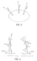
- FIG. 3 is a sectional view through a polymer dispersed cholesteric domain showing that portions of incident light 54 at a given wavelength will become reflected light 56.
- the encapsulation process provides a pressure resistant material that improves the viewing angle of the cholesteric liquid crystal.
- the first surface of light modulating layer 30 is coated over first transparent conductor 20 to provide a 10-micron thick polymer dispersed cholesteric coating.
- Other organic binders such as polyvinyl alcohol (PVA) or polyethylene oxide (PEO) can be used as the polymeric agent. Such compounds are can be coated on equipment associated with photographic films.
- FIG. 4 shows two stable states of cholesteric liquid crystals.
- a high planar voltage V2 been applied and quickly switched to zero potential, which applies and electric field that converts cholesteric liquid crystal to planar liquid crystal 50.
- Portions of incident light 54 striking planar liquid crystal 50 becomes reflected light 56 to create a bright image.
- a lower focal-conic voltage V1 applies an electric field that converts cholesteric liquid crystal to transparent focal-conic liquid crystal 52.
- Incident light 54 striking focal-conic liquid crystal 52 is transmitted.
- a light absorber 58 will absorb incident light 54 to create a dark image in areas having focal-conic liquid crystal 52.
- first transparent conductor 20 is transparent ITO.
- planar voltage V2 should be an 80 volt pulse for approximately 20 milliseconds converts cholesteric liquid crystals into the planar state.
- a pulse of about half the field strength, or 5 volts per micron converts the liquid crystal to the focal-conic state. If field carrying electrodes are spaced apart by a dielectric layer, then the field strength is reduced.
- Dielectric layer 40 is screen printed over light modulating layer 30.
- Dielectric layer 40 can be a 25 micron thick layer of Electrodag 25208 screen printable, UV curable dielectric coating from Acheson Corporation. The material is thermoplastic that is screen printable and hardens exposed to 0.3-0.6 joules/cm 2 of ultra violet radiation.
- a dielectric layer 40 screen printed at 25 microns thickness reduces the field strength to reduce planar pulse to less than the 5 volts per micron focal-conic field strength. Openings 41 in dielectric layer 40 to define image areas, which are coincident with the openings 41. Since the image is viewed through substrate 15, the indicia are mirror-imaged.
- Second conductors 42 are then printed over dielectric layer 40.
- Second conductors 42 can be formed of a 25 micron thick layer of Electrodag 423SS screen printable electrical conductive material from Acheson Corporation. The material is finely divided graphite particles in a thermoplastic resin. The effective sheet conductivity of a 25 micron printed layer is than 250 ohms per square. Such a layer is light absorbing, typically having an optical density of greater than 2.0 D. The light absorbing property of the second conductor 42 is adequate to serve as light absorber 58 for the cholesteric liquid crystal material.
- second conductor 42 In each of the image areas under openings 41, second conductor 42 directly contacts light modulating layer 30.
- a planar voltage V2 applied between first transparent conductor 20 and second conductor 42 in an image area will have a10 volts per micron field strength and convert cholesteric liquid crystals in light modulating layer 30 to planar liquid crystals 50.
- Areas having a 25 micron thick dielectric layer 40 will only experience 2.8 volts per micron and cannot be switched to the planar state if a 100 volt pulse is applied between first transparent conductor 20 and second conductor 42.
- the display 10 is arranged so that display 10 can be viewed only through the transparent substrate.
- An adhesive 46 is applied to the back of the label, which bonds display 10 to media cassette 12.
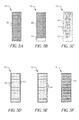
- FIGS. 5A-5F The process for manufacturing displays 10 is shown in FIGS. 5A-5F.
- FIG. 5A is a rear view of a substrate 15 supporting first transparent conductor 20 and light modulating layer 30.
- FIG. 5B is the structure from FIG. 5A after removal of a portion of light modulating layer 30 to reveal first transparent conductor 20. In the case of a gelatin and liquid crystal emulsion, light modulating layer 30 is removed by immersion in water and mechanical agitation.
- FIG. 5C is the structure of FIG. 5B after being printed with dielectric layer 40 having openings 41 defining image areas. Openings 41 in dielectric layer 40 expose areas of first transparent conductor 20.
- FIG. 5D is the structure of FIG. 5C having a second conductor 42 printed over each indicia of display 10. Through holes 43 are perforated through the entire structure outside of the indicia but through each second conductor 42.
- FIG. 5E is the display 10 of FIG. 5D, after application of thin, metallic contact pads 44. Contact pads 44 can be 25 micron gold plated copper sheets having a conductive adhesive that bonds each contact pad 44 over each through hole 43.
- FIG. 5F is the display 10 of FIG. 5E further including an adhesive 46, such as a contact adhesive, coated over the display 10. The completed display 10 of FIG. 5F can be attached to an A/V cassette. The top nine contacts of the display correspond to the 7 days of the week and the morning and evening portions of each day. The bottom contact pad 44 provides an electrical ground to first transparent conductor 20.
- FIG. 6A is a sectional view of display 10 showing electrical interconnect detail for the indicia.
- Contact 60 passes through hole 43 and engages contact pad 44.
- a contact pad 44 is bonded to each second conductor 42 for each indicia.
- FIG. 6B is a sectional view of the electrical interconnection to first transparent conductor 20. Contact 60 passes through hole 43 to connect with contact pad 44. Because dielectric layer 40 is not printed in the area and light modulating layer 30 has been removed, contact pad 44 is connected to first transparent conductor 20 to provide a ground field under each indicia.
- FIG. 7 is an electrical schematic of the circuitry used to write display 10. Contacts 60 pass through holes 43 to engage contact pads 44 as shown in FIGS. 6A and 6B. In FIG. 7, contact is made to the right most segment and connects first transparent conductor 20 to ground. The other segments are electrically connected to display drive 66.
- Power supply 62 generates two voltages, a first planar driving voltage and a second focal-conic voltage.
- a voltage select circuit 64 is used to select one of the two voltages.
- Voltage select circuit 64 can be as simple as a resistor network and a switching transistor. Control signals are applied to the voltage select circuit 64 and also to display drive 66.
- Display drive 66 is used to apply the selected voltage to appropriate segments of the display 10.
- Display drive 66 operates on a selected voltage from voltage selector 64 and applies either a ground or selected voltage to contacts 60.
- Display drive 66 can for example be embodied in a commercially available device known as HV57908PG from Supertex, Inc. of Sunnyvale, California.
- FIG. 8 is a diagram of the voltage waveform applied by display drive 66 to drive display 10.
- Voltage select circuit 64 is first set to the lower, focal-conic voltage V1 and all contacts 60 connected to second conductor 42 are receive a pulse of focal-conic voltage V1 to clear any reflective image from display 10.
- Voltage select circuit 64 is then set to apply a higher planar voltage V2 to display drive 66.
- Display drive 66 is then switched to apply planar voltage V2 across selected segments that are to be placed in the reflective, planar state. Those segments that are to remain non-reflective are not switched.
- the waveform shows the sequence of voltages that are used to write indicia into the planar state. Planar voltage V2 is omitted to maintain indicia in the clear focal-conic state.
- the drive method is a simple method of erasing and re-writing display 10
Landscapes
- Physics & Mathematics (AREA)
- Nonlinear Science (AREA)
- Chemical & Material Sciences (AREA)
- Crystallography & Structural Chemistry (AREA)
- General Physics & Mathematics (AREA)
- Optics & Photonics (AREA)
- Liquid Crystal (AREA)
- Liquid Crystal Display Device Control (AREA)
- Devices For Indicating Variable Information By Combining Individual Elements (AREA)
Abstract
Description
Claims (10)
- A rewritable display, comprising:a) a transparent substrate;b) a first transparent conductor over such substrate;c) a layer including cholesteric liquid crystal material;d) a dielectric layer having openings;e) a second conductor provided over the dielectric layer and into the openings to be in contact with the cholesteric liquid crystal bearing layer which is effective at the position in such openings to be in at least first and second optical states so that written and viewed, be electrically changed by providing appropriate electrical fields to the material; andf) means for electrically addressing the cholesteric liquid crystal layer to erase previous information and writing appropriate information.
- The rewritable display of claim 1 further including:g) means for attaching the display to an article so that the display functions as a label.
- The rewritable display in claim 1 wherein the display can be viewed only through the transparent substrate.
- The rewritable display of claim 1 further including a second conductor which is electrically connected to the first transparent conductor.
- A rewritable display, comprising:a) a plurality of electrically addressable segments, each such segment including a transparent substrate, a first transparent conductor over such substrate, a layer including cholesteric liquid crystal material, a dielectric layer having openings and a second conductor provided over the dielectric layer and into the openings to be in contact with the cholesteric liquid crystal bearing layer which is effective at the position of each such opening to be in at least first and second optical states so that information can be written, rewritten and viewed by providing appropriate electrical fields to the material; andb) means for selectively electrically addressing the cholesteric liquid crystal layer in each segment to erase previous information and writing appropriate information.
- The rewritable display of claim 5 further including:g) means for attaching the display to an article so that the display functions as a label.
- The rewritable display in claim 5 wherein the dielectric layer in each segment includes non-transparent material so that each individual segment can be viewed only through the transparent substrate.
- The rewritable display of claim 5 further wherein one of the second conductors is electrically connected to the first transparent conductor of each segment.
- A method of making a rewritable display comprising the steps of:a) providing a first transparent conductor over a transparent substrate;b) coating a layer including cholesteric liquid crystal material over the first transparent conductor;c) depositing a dielectric layer over the liquid crystal layer and forming at least one opening in such dielectric layer;d) forming a second conductor provided over the dielectric layer and into the opening to be in contact with the cholesteric liquid crystal bearing layer which is effective at the position in such opening to be in at least first and second optical states so that written and viewed, be electrically changed by providing appropriate electrical fields to the material; ande) forming a conductive path to permit electrically addressing of the cholesteric liquid crystal layer to erase previous information and writing appropriate information.
- A method of making a rewritable display comprising the steps of:a) providing a first transparent conductor over a transparent substrate;b) coating a layer which includes cholesteric liquid crystal material over selected portions of the first transparent conductor;c) depositing a dielectric layer over the liquid crystal layer and forming a plurality of openings in such dielectric layer;d) forming second conductors to define segments provided over the dielectric layer and into the openings corresponding to each segment to be in contact with the cholesteric liquid crystal bearing layer which is effective at the position in such openings to be in at least first and second optical states so that information can be written, rewritten and viewed by providing appropriate electrical fields to the material; ande) forming a conductive path to permit electrically addressing of the cholesteric liquid crystal layer to erase previous information and writing appropriate information.
Applications Claiming Priority (2)
| Application Number | Priority Date | Filing Date | Title |
|---|---|---|---|
| US799220 | 1991-11-27 | ||
| US09/799,220 US6829045B2 (en) | 2001-03-05 | 2001-03-05 | Rewritable display having a dielectric spacing layer |
Publications (2)
| Publication Number | Publication Date |
|---|---|
| EP1239324A2 true EP1239324A2 (en) | 2002-09-11 |
| EP1239324A3 EP1239324A3 (en) | 2003-09-03 |
Family
ID=25175336
Family Applications (1)
| Application Number | Title | Priority Date | Filing Date |
|---|---|---|---|
| EP02075712A Withdrawn EP1239324A3 (en) | 2001-03-05 | 2002-02-21 | A rewritable display having a dielectric spacing layer |
Country Status (3)
| Country | Link |
|---|---|
| US (1) | US6829045B2 (en) |
| EP (1) | EP1239324A3 (en) |
| JP (1) | JP2002365667A (en) |
Cited By (2)
| Publication number | Priority date | Publication date | Assignee | Title |
|---|---|---|---|---|
| GB2418206A (en) * | 2004-08-25 | 2006-03-22 | Konica Minolta Holdings Inc | Rewritable display medium |
| WO2006042737A1 (en) * | 2004-10-18 | 2006-04-27 | Ecsibeo Ab | Cholesteric liquid crystal display (lcd) device, and method for its production |
Families Citing this family (2)
| Publication number | Priority date | Publication date | Assignee | Title |
|---|---|---|---|---|
| US7104448B2 (en) * | 2002-10-29 | 2006-09-12 | Eastman Kodak Company | Docking station for writing to electronically writable display |
| US7689459B2 (en) * | 2003-09-24 | 2010-03-30 | Industiral Technology Research Institute | Card with embedded bistable display having short and long term information |
Family Cites Families (10)
| Publication number | Priority date | Publication date | Assignee | Title |
|---|---|---|---|---|
| NL7800584A (en) * | 1978-01-18 | 1979-07-20 | Philips Nv | DISPLAY DEVICE. |
| US4435047A (en) | 1981-09-16 | 1984-03-06 | Manchester R & D Partnership | Encapsulated liquid crystal and method |
| EP0153729B1 (en) * | 1984-02-27 | 1989-05-10 | TDK Corporation | Optical recording medium |
| US5040296A (en) | 1985-11-15 | 1991-08-20 | Wesco Ventures, Inc. | Erasable label |
| DE69229003T2 (en) | 1992-05-18 | 1999-10-21 | Kent State University, Kent | LIQUID CRYSTALINE, LIGHT-MODULATING DEVICE AND MATERIAL |
| TW412744B (en) * | 1996-02-13 | 2000-11-21 | Dainippon Printing Co Ltd | Device with display portion capable of rewriting |
| US5727818A (en) | 1996-03-28 | 1998-03-17 | Schmeida; Peter | Erasable label kit |
| JPH10144048A (en) | 1996-11-12 | 1998-05-29 | Sony Corp | Cassette label and video cassette tape |
| JP2000090229A (en) * | 1998-07-13 | 2000-03-31 | Minolta Co Ltd | Information recording and display card and information recording and display system using the same |
| US6215540B1 (en) * | 1998-08-10 | 2001-04-10 | Eastman Kodak Company | Light modulating layer with different transmissive states with conductive pixel areas formed from a photosensitive layer |
-
2001
- 2001-03-05 US US09/799,220 patent/US6829045B2/en not_active Expired - Lifetime
-
2002
- 2002-02-21 EP EP02075712A patent/EP1239324A3/en not_active Withdrawn
- 2002-03-04 JP JP2002057866A patent/JP2002365667A/en not_active Withdrawn
Cited By (6)
| Publication number | Priority date | Publication date | Assignee | Title |
|---|---|---|---|---|
| GB2418206A (en) * | 2004-08-25 | 2006-03-22 | Konica Minolta Holdings Inc | Rewritable display medium |
| US7344763B2 (en) | 2004-08-25 | 2008-03-18 | Konica Minolta Holdings, Inc. | Display medium |
| GB2418206B (en) * | 2004-08-25 | 2009-09-23 | Konica Minolta Holdings Inc | Rewritable display medium comprising liquid crystals dispersed in a binder |
| WO2006042737A1 (en) * | 2004-10-18 | 2006-04-27 | Ecsibeo Ab | Cholesteric liquid crystal display (lcd) device, and method for its production |
| CN100480828C (en) * | 2004-10-18 | 2009-04-22 | 拉谢扎·科米托弗 | Cholesteric Liquid Crystal Display (LCD) device and method of fabricating the same |
| US7916255B2 (en) | 2004-10-18 | 2011-03-29 | Lachezar Komitov | Cholesteric liquid crystal display (LCD) device, and method for its production |
Also Published As
| Publication number | Publication date |
|---|---|
| US6829045B2 (en) | 2004-12-07 |
| EP1239324A3 (en) | 2003-09-03 |
| JP2002365667A (en) | 2002-12-18 |
| US20020135707A1 (en) | 2002-09-26 |
Similar Documents
| Publication | Publication Date | Title |
|---|---|---|
| US7116287B2 (en) | Drive for cholesteric liquid crystal displays | |
| US6853412B2 (en) | Transaction card with memory and polymer dispersed cholesteric liquid crystal display | |
| US9651813B2 (en) | Liquid crystal paper | |
| US7532260B2 (en) | Cholesteric liquid crystal display system | |
| US8009263B2 (en) | Bistable display | |
| EP1394803A2 (en) | Mechanically scrollable display | |
| EP1058147A2 (en) | Multi-layer dual-polarity light modulating sheet | |
| US7307608B2 (en) | Unipolar drive chip for cholesteric liquid crystal displays | |
| US20030202136A1 (en) | Display having front contacts and printable area | |
| US6215540B1 (en) | Light modulating layer with different transmissive states with conductive pixel areas formed from a photosensitive layer | |
| US6829045B2 (en) | Rewritable display having a dielectric spacing layer | |
| US6710760B1 (en) | Unipolar drive for cholesteric liquid crystal displays | |
| US6690447B1 (en) | Liquid-crystal display comprising a dielectric layer between electrodes and methods for making the same | |
| EP1239440B1 (en) | Rewritable erasable labels | |
| US8334966B2 (en) | Method of forming a bistable watermark | |
| US7129911B2 (en) | Segmented display having uniform optical properties | |
| US20080267034A1 (en) | (Re) Writable Disk with Electrophoetic Ink Label | |
| JP2000030026A (en) | Information recording medium | |
| JP2002357806A5 (en) |
Legal Events
| Date | Code | Title | Description |
|---|---|---|---|
| PUAI | Public reference made under article 153(3) epc to a published international application that has entered the european phase |
Free format text: ORIGINAL CODE: 0009012 |
|
| AK | Designated contracting states |
Kind code of ref document: A2 Designated state(s): AT BE CH CY DE DK ES FI FR GB GR IE IT LI LU MC NL PT SE TR |
|
| AX | Request for extension of the european patent |
Free format text: AL;LT;LV;MK;RO;SI |
|
| PUAL | Search report despatched |
Free format text: ORIGINAL CODE: 0009013 |
|
| AK | Designated contracting states |
Kind code of ref document: A3 Designated state(s): AT BE CH CY DE DK ES FI FR GB GR IE IT LI LU MC NL PT SE TR |
|
| AX | Request for extension of the european patent |
Extension state: AL LT LV MK RO SI |
|
| RIC1 | Information provided on ipc code assigned before grant |
Ipc: 7G 02F 1/1343 B Ipc: 7G 02F 1/1334 B Ipc: 7G 02F 1/1333 B Ipc: 7G 02F 1/137 A |
|
| 17P | Request for examination filed |
Effective date: 20040223 |
|
| AKX | Designation fees paid |
Designated state(s): DE FR GB |
|
| STAA | Information on the status of an ep patent application or granted ep patent |
Free format text: STATUS: THE APPLICATION HAS BEEN WITHDRAWN |
|
| 18W | Application withdrawn |
Effective date: 20051213 |