EP1239297A2 - Planar NMR coils with localized field-generating and capacitive elements - Google Patents
Planar NMR coils with localized field-generating and capacitive elements Download PDFInfo
- Publication number
- EP1239297A2 EP1239297A2 EP02004049A EP02004049A EP1239297A2 EP 1239297 A2 EP1239297 A2 EP 1239297A2 EP 02004049 A EP02004049 A EP 02004049A EP 02004049 A EP02004049 A EP 02004049A EP 1239297 A2 EP1239297 A2 EP 1239297A2
- Authority
- EP
- European Patent Office
- Prior art keywords
- coil
- magnetic field
- radio frequency
- elements
- field generating
- Prior art date
- Legal status (The legal status is an assumption and is not a legal conclusion. Google has not performed a legal analysis and makes no representation as to the accuracy of the status listed.)
- Withdrawn
Links
- 239000003990 capacitor Substances 0.000 claims abstract description 109
- 230000005291 magnetic effect Effects 0.000 claims abstract description 71
- 239000004020 conductor Substances 0.000 claims description 73
- 239000000758 substrate Substances 0.000 claims description 17
- 239000002887 superconductor Substances 0.000 claims description 15
- 238000000151 deposition Methods 0.000 claims 1
- 238000004519 manufacturing process Methods 0.000 claims 1
- 238000000034 method Methods 0.000 claims 1
- 239000000523 sample Substances 0.000 abstract description 51
- 238000005481 NMR spectroscopy Methods 0.000 abstract description 19
- 229910052751 metal Inorganic materials 0.000 description 11
- 239000002184 metal Substances 0.000 description 10
- 230000008901 benefit Effects 0.000 description 8
- 239000010409 thin film Substances 0.000 description 7
- 230000015556 catabolic process Effects 0.000 description 6
- 239000010408 film Substances 0.000 description 6
- 239000000463 material Substances 0.000 description 6
- 238000013461 design Methods 0.000 description 5
- 230000005684 electric field Effects 0.000 description 5
- 230000003068 static effect Effects 0.000 description 5
- 230000005415 magnetization Effects 0.000 description 4
- 230000035945 sensitivity Effects 0.000 description 4
- 238000001514 detection method Methods 0.000 description 3
- 238000000386 microscopy Methods 0.000 description 3
- OKTJSMMVPCPJKN-UHFFFAOYSA-N Carbon Chemical compound [C] OKTJSMMVPCPJKN-UHFFFAOYSA-N 0.000 description 2
- 229910052799 carbon Inorganic materials 0.000 description 2
- 230000008878 coupling Effects 0.000 description 2
- 238000010168 coupling process Methods 0.000 description 2
- 238000005859 coupling reaction Methods 0.000 description 2
- 239000013078 crystal Substances 0.000 description 2
- 230000000694 effects Effects 0.000 description 2
- 238000002595 magnetic resonance imaging Methods 0.000 description 2
- 230000003071 parasitic effect Effects 0.000 description 2
- 238000000926 separation method Methods 0.000 description 2
- RYGMFSIKBFXOCR-UHFFFAOYSA-N Copper Chemical compound [Cu] RYGMFSIKBFXOCR-UHFFFAOYSA-N 0.000 description 1
- 230000005540 biological transmission Effects 0.000 description 1
- 239000000919 ceramic Substances 0.000 description 1
- 230000001010 compromised effect Effects 0.000 description 1
- 238000010276 construction Methods 0.000 description 1
- 238000001816 cooling Methods 0.000 description 1
- 229910052802 copper Inorganic materials 0.000 description 1
- 239000010949 copper Substances 0.000 description 1
- 230000003247 decreasing effect Effects 0.000 description 1
- 230000007547 defect Effects 0.000 description 1
- 238000006731 degradation reaction Methods 0.000 description 1
- 230000005292 diamagnetic effect Effects 0.000 description 1
- 230000005284 excitation Effects 0.000 description 1
- 230000007717 exclusion Effects 0.000 description 1
- 150000002739 metals Chemical class 0.000 description 1
- 238000012986 modification Methods 0.000 description 1
- 230000004048 modification Effects 0.000 description 1
- 230000003094 perturbing effect Effects 0.000 description 1
- 238000012545 processing Methods 0.000 description 1
- 238000005057 refrigeration Methods 0.000 description 1
- 238000011160 research Methods 0.000 description 1
- 229910052594 sapphire Inorganic materials 0.000 description 1
- 239000010980 sapphire Substances 0.000 description 1
- 239000002356 single layer Substances 0.000 description 1
- 230000003595 spectral effect Effects 0.000 description 1
- 238000012546 transfer Methods 0.000 description 1
Images




Classifications
-
- G—PHYSICS
- G01—MEASURING; TESTING
- G01R—MEASURING ELECTRIC VARIABLES; MEASURING MAGNETIC VARIABLES
- G01R33/00—Arrangements or instruments for measuring magnetic variables
- G01R33/20—Arrangements or instruments for measuring magnetic variables involving magnetic resonance
- G01R33/28—Details of apparatus provided for in groups G01R33/44 - G01R33/64
- G01R33/32—Excitation or detection systems, e.g. using radio frequency signals
- G01R33/34—Constructional details, e.g. resonators, specially adapted to MR
- G01R33/341—Constructional details, e.g. resonators, specially adapted to MR comprising surface coils
-
- G—PHYSICS
- G01—MEASURING; TESTING
- G01R—MEASURING ELECTRIC VARIABLES; MEASURING MAGNETIC VARIABLES
- G01R33/00—Arrangements or instruments for measuring magnetic variables
- G01R33/20—Arrangements or instruments for measuring magnetic variables involving magnetic resonance
- G01R33/28—Details of apparatus provided for in groups G01R33/44 - G01R33/64
- G01R33/32—Excitation or detection systems, e.g. using radio frequency signals
- G01R33/34—Constructional details, e.g. resonators, specially adapted to MR
- G01R33/34046—Volume type coils, e.g. bird-cage coils; Quadrature bird-cage coils; Circularly polarised coils
- G01R33/34061—Helmholtz coils
-
- G—PHYSICS
- G01—MEASURING; TESTING
- G01R—MEASURING ELECTRIC VARIABLES; MEASURING MAGNETIC VARIABLES
- G01R33/00—Arrangements or instruments for measuring magnetic variables
- G01R33/20—Arrangements or instruments for measuring magnetic variables involving magnetic resonance
- G01R33/28—Details of apparatus provided for in groups G01R33/44 - G01R33/64
- G01R33/32—Excitation or detection systems, e.g. using radio frequency signals
- G01R33/34—Constructional details, e.g. resonators, specially adapted to MR
- G01R33/34007—Manufacture of RF coils, e.g. using printed circuit board technology; additional hardware for providing mechanical support to the RF coil assembly or to part thereof, e.g. a support for moving the coil assembly relative to the remainder of the MR system
-
- G—PHYSICS
- G01—MEASURING; TESTING
- G01R—MEASURING ELECTRIC VARIABLES; MEASURING MAGNETIC VARIABLES
- G01R33/00—Arrangements or instruments for measuring magnetic variables
- G01R33/20—Arrangements or instruments for measuring magnetic variables involving magnetic resonance
- G01R33/28—Details of apparatus provided for in groups G01R33/44 - G01R33/64
- G01R33/32—Excitation or detection systems, e.g. using radio frequency signals
- G01R33/34—Constructional details, e.g. resonators, specially adapted to MR
- G01R33/34015—Temperature-controlled RF coils
- G01R33/34023—Superconducting RF coils
-
- G—PHYSICS
- G01—MEASURING; TESTING
- G01R—MEASURING ELECTRIC VARIABLES; MEASURING MAGNETIC VARIABLES
- G01R33/00—Arrangements or instruments for measuring magnetic variables
- G01R33/20—Arrangements or instruments for measuring magnetic variables involving magnetic resonance
- G01R33/28—Details of apparatus provided for in groups G01R33/44 - G01R33/64
- G01R33/32—Excitation or detection systems, e.g. using radio frequency signals
- G01R33/34—Constructional details, e.g. resonators, specially adapted to MR
- G01R33/34092—RF coils specially adapted for NMR spectrometers
Definitions
- This invention relates to RF probes for nuclear magnetic resonance (NMR) spectroscopy and microscopy and, more particularly, to resonant coils for the transmission and reception of NMR signals.
- NMR nuclear magnetic resonance
- a sample is placed in a static magnetic field which causes atomic nuclei within the sample to align in the direction of the field.
- Transmit and receive coils which may be combined in a single coil or set of coils, are placed in the probe positioned close to the sample.
- the transmit coils apply an RF magnetic field orthogonal to the direction of the static magnetic field, perturbing the alignment of the nuclei.
- the transmit signal is then turned off, and the resonant RF signal of the sample is detected by the receiver coil.
- the sensitivity of the spectrometer depends on a number of factors, including the strength of the static field, the closeness of the coupling between the RF coils and the sample, and the resistance of the RF coil.
- HTS high temperature superconductor
- U.S. Pat. No. 5,258,710 to Black also describes HTS thin-film receiver coils for NMR microscopy.
- Black discloses several embodiments, including split ring, solenoidal, saddle coils, birdcage coils and coils described as "Helmholtz pairs.”
- Black's embodiments are essentially conventional NMR coil designs and do not address the unique characteristics of high-temperature superconductor materials. Superconductors are very attractive for use in these coils. They have very low resistance at radio frequencies and, hence, produce little noise. Even so, to obtain high signal-to-noise ratio (SNR), the coils must be as close as possible to the sample.
- SNR signal-to-noise ratio
- Thin-film HTS coils offer design and processing challenges not present with normal-metal coils.
- high-temperature superconductors are perovskite ceramics, which require a well-oriented crystal structure for optimum performance. Such orientation is extremely difficult to achieve on a nonplanar substrate.
- such coils are preferably deposited epitaxially on a planar substrate. This makes the achievement of a high filling factor more challenging. It is also desirable for the coil to be deposited in a single layer of superconducting film, without crossovers.
- the coil must be able to handle relatively high currents while producing a uniform magnetic field and avoiding distortion of the B 0 field of the magnet.
- U.S. Pat. No. 5,565,778 to Brey, et al. discloses a number of different configurations of a probe for NMR spectroscopy. Each of these configurations uses a coil having conductors mounted on a planar substrate. The conductors are arranged such that the coil includes at least one interdigital capacitor. That is, interleaved conductors having a constant spacing between them are located on the substrate. Each conductor surrounds a central sample location and lies closely adjacent to at least one other conductor. None of the conductors completely surrounds the sample location on its own, but the conductors are in an alternating arrangement such that adjacent conductors have respective breaks in their conductive paths at different radial positions relative to the sample location. This results in a capacitive configuration that forms a coil surrounding the sample location.
- a magnetic resonance radio frequency resonator that makes use of a particularly efficient coil configuration.
- the resonator generates a radio frequency magnetic field in an active sample volume, and includes a planar substrate on which is deposited a conductive material.
- the conductive material is superconducting, and is preferably a high-temperature superconductor. It is deposited on the dielectric substrate so as to form a plurality of nested current carrying loops, each of which has magnetic field generating elements and interdigital capacitor elements. These elements are arranged to form a substantially closed geometric path surrounding an inner region that lies adjacent to the active volume, and that is essentially oblong in shape.
- the shape is longer along a major axis than it is along a minor axis perpendicular to the major axis.
- most or all of the capacitor elements are located in the current carrying loop farther from a center of the oblong shape than the magnetic field generating elements.
- the magnetic field generating elements run substantially parallel to the major axis of the oblong shape.
- the capacitor elements run perpendicular to the major axis.
- the capacitor elements comprise conducting fingers that are separated by non-conducting gaps.
- the magnetic field generating elements vary in length relative to their distance from a center of the oblong shape.
- the capacitor elements may also have different lengths relative to their distance from the center of the oblong shape. Typically, this would result from the electrical connection between individual magnetic field generating elements and their corresponding capacitor elements, which results in the outer elements being longer than the inner ones. Such an arrangement may therefore result in an overall space occupied by the magnetic field generating elements being essentially trapezoidal in shape.
- each magnetic field generating element is connected to a plurality of capacitor elements, while in another embodiment, each capacitor element is connected to a plurality of magnetic field generating elements.
- the total number of capacitors formed by the loops may also vary from one embodiment to another, typically depending on the necessary resonant frequency.
- the capacitors are arranged in series with each other and with the magnetic field generating elements, and may total, for example, two or four.
- One embodiment uses just a single capacitor formed by the capacitor elements.
- a variation of the present invention that is particularly useful for a one-capacitor coil makes use of sub-coils, each of which incorporates a plurality of the magnetic field generating elements and the interdigital capacitor elements.
- the capacitor elements in such an embodiment would be located to both sides of the minor axis of the coil. This provides the coil with a good degree of symmetry.
- the location of capacitor elements may alternate between sub-coils, such that the capacitor elements of a first sub-coil are located to the opposite side of the oblong shape from the capacitor elements of any sub-coil immediately adjacent to it.
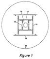
- FIG. 1 is a schematic cross sectional view of a triple resonance superconducting probe for NMR spectroscopy.
- FIG. 2 is a schematic front view of the conductor distribution for a superconducting coil for a superconducting NMR probe according to the present invention.
- FIG. 2A is an enlarged view of a section of the coil of FIG. 2.
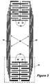
- FIG. 3 is a schematic front view of the conductor distribution of a high frequency coil for an NMR probe according to the present invention.
- FIG. 3A is an enlarged view of a section of the coil of FIG. 3.
- FIG. 4 is a schematic front view of the conductor distribution of a single capacitor superconducting coil for an NMR probe in which the coil has multiple nested sub-coils.
- FIG. 4A is an enlarged view of a section of the coil of FIG. 4.
- FIG. 5 is a schematic front view of the conductor distribution of a superconducting coil for an NMR probe in which the coil has a relatively long profile.
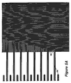
- FIG. 5A is an enlarged view of a section of the coil of FIG. 5.
- FIG. 1 A possible use for an NMR probe coil according to the present invention is shown in FIG. 1.
- the figure is shown in cross section, and depicts four sets of coil pairs 12, 14, 16, 18 surrounding a sample volume 10.
- the configuration shown may be referred to as a "triple-resonance" probe and may be used, for example, for direct observation of 1 H (coil pair 12), decoupling of 13 C and 15 N (coil pairs 14 and 16) and 2 H field lock (coil pair 18).
- an RF shield 20 is also shown in the art.
- each of the coils has a finite, but negligible, thickness perpendicular to the z-direction, and resides primarily in a plane parallel to the z-direction.
- the planes in which the two coils of a given pair reside are parallel to each other, with the sample volume 10 between them.
- FIG. 2 Shown in FIG. 2 is a schematic view of a first coil embodiment.
- the view is schematic partly in that it is shown with conductors at an exaggerated scale. That is, in order to depict clearly the configuration of the coil conductors, they are shown much thicker in the drawing figures, and with a correspondingly lower number of conductors per coil.
- two interdigital capacitors are used, one above the active sample volume and one below it.
- the capacitors are in series, and consist of horizontal conductors 24, which are also referred to herein as "fingers.”
- the capacitors are electrically connected to vertical elements 22. All conductors of the coil are a high-temperature superconducting material, and are mounted on an appropriate substrate, such as sapphire.
- the crystal substrate is epitaxially grown and, as known in the art, the HTS film is epitaxially grown on the crystalline substrate, which is chosen for having a lattice spacing that is appropriate for the HTS material.
- the vertical conductors are straight, and of uniform width. They are separated from one another by only enough of a gap to suppress the magnetization of the superconducting film.
- Each of the vertical elements 22 is connected to horizontal conductors 24 at the top and/or bottom of the coil.
- the vertical elements on each side of the coil are also electrically connected to one another by optional conductive nodes 23.
- the capacitors are located at the "top” and "bottom” of the coil.
- Sample containers tend to be oblong in shape, that is, longer in one direction than in a perpendicular direction. Therefore, coils are typically also oblong, and can be described relative to a major and a minor axis.
- the major axis extends through the center of the sample region along the longer dimension of the coil, while the minor axis extends through the center of the sample region along the shorter dimension of the coil.
- the "top” and “bottom” of the coil are those coil portions that intersect the major coil axis.
- the capacitors are segregated to the top and bottom of the coil, and the vertical elements along the coil sides are used as the primary RF magnetic field generating components. This arrangement retains the benefit provided by the capacitors, while keeping them away from the sides of the coil, where they would otherwise limit the magnetic field generating capacity of the vertical elements.
- each vertical element 22 may be connected to only half of the fingerlets that make up one finger in a capacitor.
- each of the vertical conductors 22 is connected to two horizontal elements 24.
- FIG. 2A is an enlarged view of the region 26 identified in FIG. 1.
- each pair of fingers that extend from a given vertical conductor 22 surround one of the fingers from the other side of the coil, thus creating a capacitive interleaving of the conductors from the two sides of the coil.
- the length of the fingers increases away from the center of the coil.
- the vertical conductors of the coil are necessarily different distances from the center of the coil, and so each contacts its respective fingers further from the major axis of the coil.
- the capacitors of the coil have an overall trapezoidal shape. This geometry helps to maximize the capacitive connection between the two sides of the coil, while maintaining good symmetry across the coil.
- each capacitor conductor is connected to the vertical conductor array on one side of the coil, and lies adjacent to at least one conductor that is connected to the conductor array on the opposite side of the coil. Except for a finite, but negligible, thickness of the conductors, the coil is located in the plane of the drawing page. As shown in the figures, the conductors in the vertical conductor array are straight and of uniform width. As mentioned above, the vertical conductors 22 are separated from one another by a small amount (a "gaplet") so as to suppress the magnetization effects that would otherwise result from the superconducting material. However, by maximizing the width of the vertical elements, the amount of current that may be passed through the coil is also maximized, providing for the strongest possible field.
- the fingers 24 can be thinner and further spaced apart.
- the separation between the fingers is maximized to reduce the electric field generated between adjacent fingers, while allowing for the same voltage drop as if they were closer together.
- the gap between adjacent fingers can be kept constant throughout the coil so that the peak electric field is approximately the same between all of the different adjacent capacitor fingers. In this way, the breakdown voltage of the coil is maximized.
- the ends of the fingers are also curved to minimize the risk of electrostatic discharge. Preferably, the curvature is such that the ends of the fingers approximate a semicircle.
- the gaps between the fingers in the more outer parts of the capacitor are made larger, thereby increasing the breakdown voltage in the outer current loops, which are subjected to greater induced voltages.
- each vertical element 22 By carefully maintaining the dimensions of the capacitor components and the vertical conductors, consistency is achieved across the entire coil.
- the current flowing through each vertical element 22 is uniform along its length, since it is not part of any capacitor in this region, and there is no capacitive transfer of current (except for negligible parasitic effects).
- Each of the vertical elements (except for the innermost and outermost elements) also carries approximately the same current density, since each is connected to the same value of capacitance, and has approximately the same induced voltage. However, there is a slight increase in the respective induced voltages toward the outer elements of the array. This effect may be alleviated by providing a larger gap between the fingers at the edges of the capacitor and their adjacent neighboring fingers. For example, in the embodiment of FIG.
- the uppermost finger (not shown) may be located, respectively, a distance from the next adjacent finger that is greater than the separation between the other fingers. This reduces the capacitance in these outer and inner fingers, and results in a nearly equal current in all vertical elements 22. This, in turn, allows for the peak electric field to be constant through all the various gaps between the capacitor fingers, including those on the edges of the capacitor, helping to ensure that the breakdown voltage of the coil is maximized.
- a gradation is introduced to the vertical conductors 22, with the outermost conductors being the widest. In this embodiment, there is a gradual increase in the width of the vertical conductors proceeding from the innermost to the outermost conductor on each side of the coil.
- this alternative embodiment would provide that the conductor 22a was the thinnest and conductor 22b was the thickest. This, too, ensures a more consistent current density across all the elements of the conductor array, but does not increase the breakdown voltage.
- the coil has two interdigital capacitors in series, one above the sample volume and one below it. In a probe, two such coils would be used as a pair, one to either side of the sample volume.
- a coil pair with such a configuration has been found to be particularly useful for operation at a frequency of 125.76 MHz, that of 13 C in an 11.7-Tesla magnet.
- the primary function of this coil pair is to excite, or "decouple," the carbon nuclei in a typical sample tube having a 2.5 mm outer diameter.
- a secondary function of the coil pair is to detect the resonant RF signal of these nuclei.
- the example coil may have an outer width of 10,250 ⁇ m and an inner width of 5,480 ⁇ m, with an outer length of 36,000 ⁇ m and an inner length of 13,000 ⁇ m.
- This example coil has ninety 21- ⁇ m-wide vertical elements on each side, with each vertical element connected to two 11- ⁇ m-wide capacitor fingers, the gap between adjacent capacitor fingers being 21 ⁇ m.
- FIGS. 3 and 3A show many fewer conductors than exist in the actual coil.
- the coil of this embodiment has four capacitors in series, two above the active sample volume and two below.
- a coil with this configuration may be useful, for example, to excite and detect 1 H nuclei at 600.13 MHz in a 3-mm tube in a 14.1-Tesla magnet.
- a coil for detecting 1 H (sometimes referred to as a "proton" coil) is often the innermost coil in a probe, since proton detection is quite often considered the most important.
- the resonant frequency necessary for proton detection is significantly higher than that for almost all other isotopes, particular design constraints on the coil exist. Because the necessary resonant frequency is higher, the total capacitance may be lower. This, in turn, allows the use of more capacitors and, as shown in FIG. 3, the example coil has four capacitors in series.
- the voltage of the coil is distributed among its capacitors.
- the use of four capacitors provides the option of making the overall voltage higher, since there are more capacitors to bear the load.
- a higher total current may correspondingly be produced, allowing a higher overall magnetic field intensity to be generated.
- increasing a total voltage of the coil one might take advantage of the spreading of the voltage across more capacitors by narrowing the gaps between fingers. With more capacitors, there is a lower voltage drop at each capacitor, so that the possibility of breakdown is decreased. By taking advantage of this fact by reducing the gaps between the capacitor elements, a better confinement of the electric field in the coil is achieved.
- the capacitors are located in the top and bottom of the coil.
- the capacitive fingers include those fingers 32 that extend from the vertical elements 30 of the coil.
- the center fingers 34 that extend between the fingers 32.
- the center fingers 34 are electrically connected to one another by conductor 36. This helps to ensure an equal voltage on each of the center fingers 34.
- the capacitor arrangements at the top and bottom of the coil are symmetrical about a horizontal axis passing through the center of the coil.
- the vertical elements are tapered inward at the top and bottom of the coil. That is, the vertical conductors 30 located closer to the center of the coil make contact with fingers 32 that are closer to the center of the coil, and therefore have a shorter overall length than the vertical elements to the outside. This allows the conductors further to the outside to be contoured inward around their inside neighbors, so that as one set of vertical elements terminates, the remaining vertical elements all shift inward together. This creates a stepwise tapering inward at the top and bottom of the coil. This is shown more clearly in FIG. 3A, which is an enlarged view of the region 38 of the coil that is identified in FIG. 3.
- each of the conductors is in contact with two of the adjacent horizontal fingerlets, and the fingerlets are arranged in groups of four.
- each of the groups of four makes up one finger 32 of the capacitors, so that two vertical elements are electrically connected to each of the fingers 32.
- the center fingers 34 are likewise made up of four conductors each.
- each vertical element can connect to any integral number of fingers, or even to half a finger, as in this case.
- each finger is broken up into as many fingerlets as necessary to keep each individual fingerlet narrow enough that the shimmability of the magnet is not compromised.
- an appropriate width to ensure good shimmability should be preferably less than or equal to twenty microns, although higher widths (e.g., 30 microns) may often prove satisfactory.
- connections between the vertical elements and the fingers are also made so that the total width of the fingers to which a single vertical element is connected is at least as great as the width of that vertical element itself. This ensures that the capacitor fingers do not limit the current that passes through the probe, i.e., that the capacitor fingers are not a "current bottleneck.”
- the ends of the capacitor fingers are curved, so as to minimize the peak field strength and prevent electrostatic discharge.
- the ends of the fingerlets are shaped in such a way that the end of each finger has an approximately semicircular shape.
- the example coil could be a proton coil for a 600 MHz probe with 3-mm samples.
- the example coil has an outer coil width of 6,750 ⁇ m and an inner coil width of 2,830 ⁇ m.
- the outer length of is 34,000 ⁇ m and the inner length of 13,000 ⁇ m.
- the coil has 140 11- ⁇ m-wide vertical elements on each side, with each vertical element connected to one 11- ⁇ m-wide capacitor finger. In this example, the gaps between adjacent capacitor fingers are 26 ⁇ m. With these dimensions, it is not necessary to break the capacitor fingers into fingerlets (as is shown in the figures) and, as mentioned, each vertical element is connected to an entire capacitor finger.
- FIG. 4 Another coil embodiment is shown in FIG. 4, and makes use of a coil nesting strategy to provide a single capacitor in a symmetric arrangement.
- the coil is intended to excite and detect 13 C nuclei at 125.76 MHz in a 0.8-mm inner-diameter capillary tube.
- the frequency needed is the same as that required of the coil of FIG. 1, in this embodiment, there is a much smaller sample size. Therefore, the allowed substrate width is smaller, and even a two capacitor coil is not sufficient to provide the necessary low frequency signal.
- the coil of FIG. 4 uses only a single capacitor. However, the capacitor is divided into four pieces, and the resulting "sub-coils" are concentrically nested. This nesting provides a good degree of symmetry to the coil, and results in the RF magnetic field being more homogeneous and perturbations to the static field being minimal. Moreover, undesirable fringing electric fields in the sample region are reduced.
- the sub-coils of FIG. 4 are arranged so that each one has a capacitive section at either its top or bottom, relative to the orientation of the figure.
- the relative location of the capacitive section alternates from one sub-coil to the next, such that the innermost sub-coil 40 has a capacitive section on its bottom side, while the sub-coil 42 surrounding it has its capacitive section along its top side.
- the outermost sub-coil 46 also has its capacitive section along its top side, while the sub-coil 44 it surrounds has its capacitive section along its bottom side.
- the construction of each sub-coil is the same, except that they differ in size.
- the symmetry of the coil nesting is such that the magnetic field generated within the coil is also symmetric.
- the capacitive portions of the sub-coils are all the same horizontal width, and each have the same number of capacitive fingers.
- each vertical conductor is connected to two fingers of a capacitive portion.
- This allows the vertical elements of the sub-coils to be relatively wide, while allowing the necessary gaps between capacitive fingers.
- FIG. 4A is an enlargement of the region 48 identified in FIG. 4.
- the capacitive region of each coil is defined by the overlap of the capacitor fingers 50.
- the overlap region is the same width throughout the entire coil.
- conductive sections 52 are located within the spaces between fingers outside of the range of capacitive overlap.
- the conductive islands 52 of the coil provide RF magnetic field rejection in the empty regions between the fingers. As shown, the islands vary in length depending on the distance of a particular vertical element from the overlap region of the finger to which it is connected.
- the example coil could be a carbon coil for a 600 MHz probe with 1-mm capillary samples.
- the coil has an outer width of 6,750 ⁇ m and an inner width of 3,990 ⁇ m.
- the outer length of is 25,000 ⁇ m and the inner length of 10,000 ⁇ m.
- the coil has ninety-two 12.5- ⁇ m-wide vertical elements on each side, twenty-three vertical elements on each side of each sub-coil. Each vertical element is connected to two 12.5- ⁇ m-wide capacitor fingers. In this example, the gaps between adjacent capacitor fingers are 24.5 ⁇ m.
- FIG. 5 is shown another coil embodiment.
- the vertical conductors of this coil which are located in regions 60, are not explicitly shown in the figure due to their density. Those skilled in the art, however, will understand that the regions 60 contain parallel vertical elements that connect to the fingers of the capacitors 62.
- the coil of FIG. 5 is a two-capacitor coil, and would be appropriate, for example, for 1 H excitation and detection with 3-mm samples in a 14.1-Tesla magnet. For each of the capacitors, only thirty finger pairs are needed to achieve the required capacitance.
- the different coils are not necessarily to scale relative to each other but, rather, are drawn so as to make them as descriptive as possible. Therefore, for example, while it might appear from the figures that the two-capacitor coil of FIG. 5 might have more vertical conductors than the four-capacitor coil of FIG. 3, typically the opposite is true.
- FIG. 5A Depicted in FIG. 5A is an enlarged view of the area 64 identified in FIG. 5.
- Each finger is split into two 22 ⁇ m-wide fingerlets 66, each of which connects to one 22- ⁇ m-wide vertical elements.
- the vertical spaces left by the termination of the inner vertical elements are filled by conductive islands 68.
- the length of the islands is progressively longer toward the top and bottom of the coil, so that an inner vertical edge of conductive material is constant over much of the range of each capacitor 62.
- the vertical elements are tapered inward toward the fingerlets 66.
- the tapered regions 70 shown in FIG. 5, are tapered like the tapered regions of FIG.
- each innermost conductor terminates at its respective fingerlet.
- this tapering brings an inner vertical edge of conductive material closer to the fingerlets than in the section of the capacitor closer to the coil center. This keeps the vertical elements away from the edge of a wafer upon which the coil may be fabricated. Film quality often tends to be lower near such edges and, therefore, it is preferable to maintain a minimum distance of 1.5 mm from the wafer edge when providing a layout of the coils.
- the tapering of the coils of FIGS. 3 and 5 may allow more coils to be fabricated from a single wafer.
- the example coil could be a proton coil for a 600 MHz probe with 3-mm capillary samples.
- the coil has an outer width of 6,750 ⁇ m and an inner width of 3,750 ⁇ m.
- the outer length of is 25,000 ⁇ m and the inner length of 13,000 ⁇ m.
- the coil has sixty 22- ⁇ m-wide vertical elements on each side, each connected to a 22- ⁇ m-wide fingerlet at the top of the coil and another 22- ⁇ m-wide fingerlet at the bottom of the coil.
- Each of these fingerlets forms half of one capacitor finger.
- the gaps between adjacent capacitor fingers are 53 ⁇ m.
- the vertical elements running from the top to the bottom on both sides of the coil are straight and of uniform width. They are separated by only enough gap (a "gaplet") to suppress the magnetization of the superconducting film.
- all vertical elements on each side of the coil may, at their midpoint, be connected by a common node.
- a common node may be used to connect the conductors of each sub-coil in the nested single-capacitor coil of FIGS. 4 and 4A. Each of these nodes is connected to elements of the capacitors at the top and/or bottom of the coil.
- each vertical element will be connected to one or more of the alternating fingers of capacitors.
- each vertical element may be connected to only half on the fingerlets that make up one finger in a capacitor.
- the coil design may be optimized for filling factor, depending upon the size and shape of the sample, and may be designed for any desired resonant frequency. Further, it will be appreciated that the invention is useful for NMR spectroscopy and microscopy and for magnetic resonance imaging.
Landscapes
- Physics & Mathematics (AREA)
- Condensed Matter Physics & Semiconductors (AREA)
- General Physics & Mathematics (AREA)
- Magnetic Resonance Imaging Apparatus (AREA)
Abstract
Description
Claims (18)
- A magnetic resonance radio frequency resonator that generates a radio frequency magnetic field in an active sample volume, the magnetic resonance radio frequency resonator comprising:a dielectric substrate;a conductive material deposited on the dielectric substrate and forming a plurality of nested current carrying loops each of which has magnetic field generating elements and interdigital capacitor elements, the current carrying loops forming a substantially closed geometric path surrounding an inner region that has a substantially oblong shape and lies adjacent to the active sample volume, wherein substantially all of the interdigital capacitor elements are located farther from a center of the oblong shape than the magnetic field generating elements.
- A magnetic resonance radio frequency resonator according to claim 1 wherein the conductive material is a superconductor, in particular a high temperature superconductor.
- A magnetic resonance radio frequency resonator according to claim 1 or 2 wherein the magnetic field generating elements comprise electrical conductors that run substantially parallel to a major axis of the oblong shape.
- A magnetic resonance radio frequency resonator according to claim 3 wherein the interdigital capacitor elements comprise electrical conductors that run substantially perpendicular to said major axis of the oblong shape.
- A magnetic resonance radio frequency resonator according to claim 4 wherein the interdigital capacitor elements comprise conducting fingers separated by non-conducting gaps that also extend in a direction perpendicular to said major axis.
- A magnetic resonance radio frequency resonator according to claim 3 wherein the respective lengths of the magnetic field generating elements and/or of the interdigital capacitor elements vary relative to their distance from a center of the oblong shape.
- A magnetic resonance radio frequency resonator according to claim 6 wherein, together, the magnetic field generating elements occupy a space having a substantially trapezoidal shape.
- A magnetic resonance radio frequency resonator according to anyone of the preceding claims wherein each of the magnetic field generating elements is electrically connected to a plurality of the interdigital capacitor elements.
- A magnetic resonance radio frequency resonator according to one of claims 1 to 7 wherein each of the interdigital capacitor elements is electrically connected to a plurality of the magnetic field generating elements.
- A magnetic resonance radio frequency resonator according to anyone of the preceding claims wherein the interdigital capacitor elements together make up a plurality of capacitors, in particular two or four capacitors, connected in series with the magnetic field generating elements.
- A magnetic resonance radio frequency resonator according to one of claims 1 to 9 wherein the interdigital capacitor elements together make up one capacitor connected in series with the magnetic field generating elements.
- A magnetic resonance radio frequency resonator according to anyone of the preceding claims wherein the resonator comprises a plurality of conductive sub-coils, each of which incorporates a plurality of said magnetic field generating elements and said interdigital capacitor elements, and wherein the capacitor elements are located to both sides of the oblong shape relative to a major axis of the oblong shape.
- A magnetic resonance radio frequency resonator according to claim 12 wherein the capacitor elements of a first sub-coil are located to an opposite side of the oblong shape from the capacitor elements of any sub-coil immediately adjacent to the first sub-coil.
- A magnetic resonance radio frequency resonator according to anyone of the preceding claims further comprising isolated conductive segments located within a portion of the space occupied by the resonator which conductive segments are not electrically connected to the current carrying loops.
- A magnetic resonance radio frequency resonator according to claim 14 wherein the isolated conductive segments vary in length relative to a distance of the segments from a center of the oblong shape.
- A magnetic resonance radio frequency resonator according to anyone of the preceding claims wherein the capacitive elements include capacitive fingers electrically connected to the magnetic field generating elements, and central capacitive fingers that provide capacitive connection between two sets of said capacitive fingers located on opposite sides of a major axis of the oblong shape.
- A resonant magnetic field coil for an NMR spectrometer that generates a radio frequency magnetic field in an active sample volume, the coil comprising:a planar dielectric substrate;conductive material, in particular a superconductor, preferably a high-temperature superconductor, deposited on the dielectric substrate and forming a plurality of nested current carrying loops each of which has magnetic field generating elements and interdigital capacitor elements, the current carrying loops forming a substantially closed geometric path surrounding an inner region that has a substantially oblong shape and lies adjacent to the active sample volume, wherein the magnetic field generating elements comprise electrical conductors that run substantially parallel to a major axis of the oblong shape and the interdigital capacitor elements comprise electrical conductors that run substantially perpendicular to said major axis of the oblong shape such that substantially all of the interdigital capacitor elements are located farther from a center of the oblong shape than the magnetic field generating elements.
- A method of making a magnetic resonance radio frequency resonator, in particular according to one of claims 1 to 16, that generates a radio frequency magnetic field in an active sample volume, the method comprising:providing a planar dielectric substrate;depositing a conductive material on the dielectric substrate to form a plurality of nested current carrying loops each of which has magnetic field generating elements and interdigital capacitor elements, the current carrying loops forming a substantially closed geometric path surrounding an inner region that has a substantially oblong shape and lies adjacent to the active sample volume, wherein substantially all of the interdigital capacitor elements are located farther from a center of the oblong shape than the magnetic field generating elements.
Applications Claiming Priority (2)
| Application Number | Priority Date | Filing Date | Title |
|---|---|---|---|
| US09/803,199 US6556013B2 (en) | 2001-03-09 | 2001-03-09 | Planar NMR coils with localized field-generating and capacitive elements |
| US803199 | 2001-03-09 |
Publications (2)
| Publication Number | Publication Date |
|---|---|
| EP1239297A2 true EP1239297A2 (en) | 2002-09-11 |
| EP1239297A3 EP1239297A3 (en) | 2004-12-22 |
Family
ID=25185869
Family Applications (1)
| Application Number | Title | Priority Date | Filing Date |
|---|---|---|---|
| EP02004049A Withdrawn EP1239297A3 (en) | 2001-03-09 | 2002-02-23 | Planar NMR coils with localized field-generating and capacitive elements |
Country Status (3)
| Country | Link |
|---|---|
| US (2) | US6556013B2 (en) |
| EP (1) | EP1239297A3 (en) |
| JP (1) | JP2002328156A (en) |
Cited By (8)
| Publication number | Priority date | Publication date | Assignee | Title |
|---|---|---|---|---|
| WO2003029834A1 (en) * | 2001-09-28 | 2003-04-10 | Varian, Inc. | Nmr probe with enhanced power handling ability |
| US6556013B2 (en) * | 2001-03-09 | 2003-04-29 | Bruker Biospin Corp. | Planar NMR coils with localized field-generating and capacitive elements |
| US6727700B2 (en) * | 2001-04-17 | 2004-04-27 | Bruker Biospin Ag | Superconducting NMR resonators generating RF magnetic fields at the sample which are substantially parallel to the plane of a resonator |
| EP1574872A3 (en) * | 2004-03-10 | 2006-03-08 | Bruker Biospin Corp. | Planar NMR rf coil with gyromagnetic arc suppression |
| EP1643261A1 (en) * | 2004-08-11 | 2006-04-05 | Hitachi, Ltd. | Nuclear magnetic resonance apparatus |
| WO2006030332A3 (en) * | 2004-09-16 | 2006-06-01 | Koninkl Philips Electronics Nv | Magnetic resonance receive coils with compact inductive components |
| GB2468359A (en) * | 2009-03-06 | 2010-09-08 | 3 Cs Ltd | Magnetic Resonance System |
| CN106802358A (en) * | 2015-11-26 | 2017-06-06 | 云南电网有限责任公司瑞丽供电局 | A kind of just detachable coil device for composite insulator detection |
Families Citing this family (44)
| Publication number | Priority date | Publication date | Assignee | Title |
|---|---|---|---|---|
| US6335622B1 (en) * | 1992-08-25 | 2002-01-01 | Superconductor Technologies, Inc. | Superconducting control elements for RF antennas |
| US6888153B2 (en) * | 2000-04-05 | 2005-05-03 | University Of Washington | Capacitive shield for containing radiofrequency magnetic fields |
| DE10203279C1 (en) * | 2002-01-29 | 2003-10-09 | Bruker Biospin Ag | Method for influencing the homogeneous static magnetic field in an NMR apparatus and associated NMR resonator |
| DE10205625C1 (en) * | 2002-02-12 | 2003-07-24 | Bruker Biospin Ag Faellanden | HF reception coil for normally-conductive nuclear magnetic resonator incorporates device for compensation of magnetic susceptibility |
| US20040041565A1 (en) * | 2002-05-08 | 2004-03-04 | Shigeru Kakugawa | NMR magnet device for solution analysis and NMR apparatus |
| US7521932B2 (en) * | 2003-05-06 | 2009-04-21 | The Penn State Research Foundation | Method and system for adjusting the fundamental symmetric mode of coupled high temperature superconductor coils |
| US6943550B2 (en) * | 2003-05-09 | 2005-09-13 | The University Of Hong Kong | High temperature superconductor tape RF coil for magnetic resonance imaging |
| US7295085B2 (en) * | 2003-08-21 | 2007-11-13 | E.I. Du Pont De Nemours And Company | Process for making high temperature superconductor devices each having a line oriented in a spiral fashion |
| US20050104593A1 (en) * | 2003-08-21 | 2005-05-19 | Laubacher Daniel B. | Nuclear quadrupole resonance detection system using a high temperature superconductor self-resonant coil |
| US7148684B2 (en) * | 2003-10-23 | 2006-12-12 | E.I. Du Pont De Nemours And Company | Method for biological identification using high temperature superconductor enhanced nuclear quadrupole resonance |
| WO2005047917A1 (en) * | 2003-11-12 | 2005-05-26 | E.I. Dupont De Nemours And Company | Detection of contraband using nuclear quadrupole resonance |
| US7332910B2 (en) * | 2003-11-24 | 2008-02-19 | E.I. Du Pont De Nemours And Company | Frequency detection system comprising circuitry for adjusting the resonance frequency of a high temperature superconductor self-resonant coil |
| US20070245374A1 (en) * | 2003-11-24 | 2007-10-18 | Inventec Corporation | Video program subtitle tex recording method and system |
| US7301344B2 (en) * | 2003-11-24 | 2007-11-27 | E.I. Du Pont De Nemours & Co. | Q-damping circuit including a high temperature superconductor coil for damping a high temperature superconductor self-resonant coil in a nuclear quadrupole resonance detection system |
| US7375525B2 (en) * | 2003-12-15 | 2008-05-20 | E.I. Du Pont De Nemours And Company | Use of multiple sensors in a nuclear quadropole resonance detection system to improve measurement speed |
| US7859264B2 (en) * | 2004-01-20 | 2010-12-28 | The University Of Houston | Superconducting loop, saddle and birdcage MRI coils capable of simultaneously imaging small nonhuman animals |
| US7355401B2 (en) * | 2004-02-04 | 2008-04-08 | E.I. Du Pont De Nemours And Company | Use of two or more sensors to detect different nuclear quadrupole resonance signals of a target compound |
| WO2005109023A2 (en) | 2004-02-04 | 2005-11-17 | E.I. Dupont De Nemours And Company | Nqr rf coil assembly comprising two or more coils which may be made from hts |
| DE102004007291B4 (en) * | 2004-02-14 | 2006-09-21 | Bruker Biospin Gmbh | Hybrid magnet arrangement |
| WO2006076004A2 (en) * | 2004-04-15 | 2006-07-20 | E. I. Dupont De Nemours And Company | Decoupling high temperature superconductor sensor arrays in nuclear quadrupole resonance detection systems |
| DE102004020167B4 (en) * | 2004-04-24 | 2012-01-05 | Bruker Biospin Ag | High-frequency resonator system with optimized current distribution in the conductor elements and method for its design |
| US7265549B2 (en) | 2004-04-30 | 2007-09-04 | E. I. Du Pont De Nemours And Company | Scanning a band of frequencies using an array of high temperature superconductor sensors tuned to the same frequency |
| WO2006073452A2 (en) * | 2004-04-30 | 2006-07-13 | E.I. Dupont De Nemours And Company | Methods and apparatus for scanning a band of frequencies by nqr using an array of high temperature superconductor sensors |
| US7279897B2 (en) * | 2004-04-30 | 2007-10-09 | E. I. Du Pont De Nemours And Company | Scanning a band of frequencies using an array of high temperature superconductor sensors tuned to different frequencies |
| US7064548B2 (en) * | 2004-04-30 | 2006-06-20 | The Boc Group, Inc. | RF probe apparatus for NMR check weighing system |
| DE102004035851B4 (en) | 2004-07-23 | 2006-11-16 | Bruker Biospin Ag | Resonator system for generating a high-frequency magnetic field |
| US7388377B2 (en) * | 2004-12-03 | 2008-06-17 | E.I. Du Pont De Nemours And Company | Method for reducing the coupling between excitation and receive coils of a nuclear quadrupole resonance detection system |
| WO2006065929A1 (en) * | 2004-12-13 | 2006-06-22 | E. I. Du Pont De Nemours And Company | Metal shield alarm in a nuclear quadrupole resonance/x-ray contraband detection system |
| EP1890596B1 (en) * | 2005-03-29 | 2013-10-02 | Dune Medical Devices Ltd. | Electromagnetic sensors for tissue characterization |
| JP4971685B2 (en) * | 2006-05-25 | 2012-07-11 | 株式会社日立製作所 | Nuclear magnetic resonance probe coil |
| JP2008233025A (en) * | 2007-03-23 | 2008-10-02 | Hitachi Ltd | NMR measurement equipment |
| DE102008035655A1 (en) * | 2007-08-23 | 2009-02-26 | Zenergy Power Gmbh | Winding body for a saddle coil winding |
| EP2601723B1 (en) | 2010-08-06 | 2020-04-22 | Auckland UniServices Limited | Inductive power receiver apparatus |
| JP2014098716A (en) * | 2014-02-19 | 2014-05-29 | Keio Gijuku | Measurement instrument and fuel battery system |
| DE102014203588B4 (en) * | 2014-02-27 | 2016-08-25 | Siemens Healthcare Gmbh | Arrangement and method for transmitting and / or receiving MRI signals for an MRI examination |
| TWI537656B (en) * | 2014-03-14 | 2016-06-11 | 群創光電股份有限公司 | Display device |
| US10324345B2 (en) | 2014-03-14 | 2019-06-18 | Innolux Corporation | Display device and display substrate |
| US9995801B2 (en) | 2014-12-02 | 2018-06-12 | University Of Kentucky Research Foundation | Static multiple-sample NMR probe |
| JP6677573B2 (en) * | 2016-05-13 | 2020-04-08 | 日本電子株式会社 | Magnetic resonance signal detection module |
| DE102016221161A1 (en) * | 2016-10-27 | 2018-05-03 | Bruker Biospin Ag | HF resonator arrangement |
| US10921399B2 (en) * | 2017-11-22 | 2021-02-16 | GE Precision Healthcare LLC | Radio frequency (RF) coil array for a magnetic resonance imaging (MRI) system for use in interventional and surgical procedures |
| US11714146B2 (en) | 2020-09-29 | 2023-08-01 | Socpra Sciences Et Genie S.E.C. | Nuclear magnetic resonance spectrometer, method of operation, and probe therefore |
| EP4053865B1 (en) * | 2021-03-02 | 2024-04-24 | Imec VZW | Trench capacitor device for a superconducting electronic circuit, superconducting qubit device and method for forming a trench capacitor device for a qubit device |
| JPWO2022249995A1 (en) * | 2021-05-25 | 2022-12-01 |
Family Cites Families (11)
| Publication number | Priority date | Publication date | Assignee | Title |
|---|---|---|---|---|
| US4723908A (en) * | 1985-05-01 | 1988-02-09 | Kranbuehl David E | Dielectric probe; method and apparatus including its use |
| US5258710A (en) | 1992-03-27 | 1993-11-02 | General Electric Company | Cryogenic probe for NMR microscopy |
| US5594342A (en) | 1992-06-01 | 1997-01-14 | Conductus, Inc. | Nuclear magnetic resonance probe coil with enhanced current-carrying capability |
| US5565778A (en) | 1992-06-01 | 1996-10-15 | Conductus, Inc. | Nuclear magnetic resonance probe coil |
| US5276398A (en) * | 1992-06-01 | 1994-01-04 | Conductus, Inc. | Superconducting magnetic resonance probe coil |
| US5585723A (en) * | 1995-03-23 | 1996-12-17 | Conductus, Inc. | Inductively coupled superconducting coil assembly |
| ATE232305T1 (en) * | 1996-12-02 | 2003-02-15 | Univ Columbia | SUPERCONDUCTIVE MULTIPLE RESONANCE PROBE |
| US6201392B1 (en) * | 1997-11-07 | 2001-03-13 | Varian, Inc. | Coplanar RF probe coil arrangement for multifrequency excitation |
| US6377047B1 (en) * | 2000-06-08 | 2002-04-23 | Varian, Inc. | Superconducting birdcage coils |
| US6556013B2 (en) * | 2001-03-09 | 2003-04-29 | Bruker Biospin Corp. | Planar NMR coils with localized field-generating and capacitive elements |
| US6590394B2 (en) * | 2001-09-28 | 2003-07-08 | Varian, Inc. | NMR probe with enhanced power handling ability |
-
2001
- 2001-03-09 US US09/803,199 patent/US6556013B2/en not_active Expired - Lifetime
-
2002
- 2002-02-23 EP EP02004049A patent/EP1239297A3/en not_active Withdrawn
- 2002-03-11 JP JP2002065888A patent/JP2002328156A/en active Pending
-
2003
- 2003-04-28 US US10/424,687 patent/US6842004B2/en not_active Expired - Lifetime
Cited By (13)
| Publication number | Priority date | Publication date | Assignee | Title |
|---|---|---|---|---|
| US6556013B2 (en) * | 2001-03-09 | 2003-04-29 | Bruker Biospin Corp. | Planar NMR coils with localized field-generating and capacitive elements |
| US6727700B2 (en) * | 2001-04-17 | 2004-04-27 | Bruker Biospin Ag | Superconducting NMR resonators generating RF magnetic fields at the sample which are substantially parallel to the plane of a resonator |
| US6590394B2 (en) | 2001-09-28 | 2003-07-08 | Varian, Inc. | NMR probe with enhanced power handling ability |
| WO2003029834A1 (en) * | 2001-09-28 | 2003-04-10 | Varian, Inc. | Nmr probe with enhanced power handling ability |
| EP1574872A3 (en) * | 2004-03-10 | 2006-03-08 | Bruker Biospin Corp. | Planar NMR rf coil with gyromagnetic arc suppression |
| US7173424B2 (en) | 2004-08-11 | 2007-02-06 | Hitachi, Ltd. | Nuclear magnetic resonance apparatus |
| EP1643261A1 (en) * | 2004-08-11 | 2006-04-05 | Hitachi, Ltd. | Nuclear magnetic resonance apparatus |
| WO2006030332A3 (en) * | 2004-09-16 | 2006-06-01 | Koninkl Philips Electronics Nv | Magnetic resonance receive coils with compact inductive components |
| US7443163B2 (en) | 2004-09-16 | 2008-10-28 | Koninklijke Philips Electronics N.V. | Magnetic resonance receive coils with compact inductive components |
| GB2468359A (en) * | 2009-03-06 | 2010-09-08 | 3 Cs Ltd | Magnetic Resonance System |
| GB2468359B (en) * | 2009-03-06 | 2013-09-11 | 3 Cs Ltd | Magnetic resonance system |
| CN106802358A (en) * | 2015-11-26 | 2017-06-06 | 云南电网有限责任公司瑞丽供电局 | A kind of just detachable coil device for composite insulator detection |
| CN106802358B (en) * | 2015-11-26 | 2023-06-30 | 云南电网有限责任公司瑞丽供电局 | Easy-to-detach radio frequency coil device for detecting composite insulator |
Also Published As
| Publication number | Publication date |
|---|---|
| US20040032262A1 (en) | 2004-02-19 |
| US20030052682A1 (en) | 2003-03-20 |
| US6556013B2 (en) | 2003-04-29 |
| US6842004B2 (en) | 2005-01-11 |
| JP2002328156A (en) | 2002-11-15 |
| EP1239297A3 (en) | 2004-12-22 |
Similar Documents
| Publication | Publication Date | Title |
|---|---|---|
| US6556013B2 (en) | Planar NMR coils with localized field-generating and capacitive elements | |
| US5585723A (en) | Inductively coupled superconducting coil assembly | |
| EP0830614B1 (en) | Nuclear magnetic resonance probe coil | |
| JP4237735B2 (en) | Resonator system | |
| JP4490966B2 (en) | High frequency MRI coil | |
| JP3066359B2 (en) | Superconducting hybrid resonator for NMR signal reception | |
| US6087832A (en) | Edge-wound solenoids and strongly coupled ring resonators for NMR and MRI | |
| US9274199B2 (en) | NMR RF probe coil exhibiting double resonance | |
| JP2002341001A (en) | Rf receiving coil device | |
| EP0990175A1 (en) | Low-inductance transverse litz foil coils | |
| JP2008527377A (en) | NMR RF coil with improved low frequency efficiency | |
| JP2007101550A (en) | Electrically symmetric NMR coil with windings connected in series | |
| EP1613974A2 (en) | Nmr probe having an inner quadrature detection coil combined with a spiral wound outer coil for irradiation | |
| JP2008527376A (en) | NMR RF coil with split movable capacitance band | |
| US12019129B2 (en) | NMR probehead | |
| US6130537A (en) | HR MAS NMR coils with magic angle capacitors | |
| US7295009B2 (en) | Planar NMR coil with gyromagnetic arc suppression | |
| US7078902B2 (en) | Radio frequency resonator system with optimized current distribution in the conducting elements | |
| US7075397B2 (en) | Coil structure for magnetic resonance imaging | |
| US8564294B2 (en) | Nuclear magnetic resonance probe comprising slit superconducting coil with normal-metal overlayer |
Legal Events
| Date | Code | Title | Description |
|---|---|---|---|
| PUAI | Public reference made under article 153(3) epc to a published international application that has entered the european phase |
Free format text: ORIGINAL CODE: 0009012 |
|
| AK | Designated contracting states |
Kind code of ref document: A2 Designated state(s): AT BE CH CY DE DK ES FI FR GB GR IE IT LI LU MC NL PT SE TR |
|
| AX | Request for extension of the european patent |
Free format text: AL;LT;LV;MK;RO;SI |
|
| PUAL | Search report despatched |
Free format text: ORIGINAL CODE: 0009013 |
|
| AK | Designated contracting states |
Kind code of ref document: A3 Designated state(s): AT BE CH CY DE DK ES FI FR GB GR IE IT LI LU MC NL PT SE TR |
|
| AX | Request for extension of the european patent |
Extension state: AL LT LV MK RO SI |
|
| 17P | Request for examination filed |
Effective date: 20050407 |
|
| AKX | Designation fees paid |
Designated state(s): CH DE GB LI |
|
| 17Q | First examination report despatched |
Effective date: 20090225 |
|
| STAA | Information on the status of an ep patent application or granted ep patent |
Free format text: STATUS: THE APPLICATION IS DEEMED TO BE WITHDRAWN |
|
| 18D | Application deemed to be withdrawn |
Effective date: 20090908 |