EP1237040A2 - Integrated optical elements - Google Patents
Integrated optical elements Download PDFInfo
- Publication number
- EP1237040A2 EP1237040A2 EP02251028A EP02251028A EP1237040A2 EP 1237040 A2 EP1237040 A2 EP 1237040A2 EP 02251028 A EP02251028 A EP 02251028A EP 02251028 A EP02251028 A EP 02251028A EP 1237040 A2 EP1237040 A2 EP 1237040A2
- Authority
- EP
- European Patent Office
- Prior art keywords
- optical
- switch module
- waveguide
- optical switch
- substrate
- Prior art date
- Legal status (The legal status is an assumption and is not a legal conclusion. Google has not performed a legal analysis and makes no representation as to the accuracy of the status listed.)
- Granted
Links
Images
















Classifications
-
- G—PHYSICS
- G02—OPTICS
- G02F—OPTICAL DEVICES OR ARRANGEMENTS FOR THE CONTROL OF LIGHT BY MODIFICATION OF THE OPTICAL PROPERTIES OF THE MEDIA OF THE ELEMENTS INVOLVED THEREIN; NON-LINEAR OPTICS; FREQUENCY-CHANGING OF LIGHT; OPTICAL LOGIC ELEMENTS; OPTICAL ANALOGUE/DIGITAL CONVERTERS
- G02F1/00—Devices or arrangements for the control of the intensity, colour, phase, polarisation or direction of light arriving from an independent light source, e.g. switching, gating or modulating; Non-linear optics
- G02F1/29—Devices or arrangements for the control of the intensity, colour, phase, polarisation or direction of light arriving from an independent light source, e.g. switching, gating or modulating; Non-linear optics for the control of the position or the direction of light beams, i.e. deflection
- G02F1/295—Analog deflection from or in an optical waveguide structure]
-
- G—PHYSICS
- G02—OPTICS
- G02B—OPTICAL ELEMENTS, SYSTEMS OR APPARATUS
- G02B6/00—Light guides; Structural details of arrangements comprising light guides and other optical elements, e.g. couplings
- G02B6/10—Light guides; Structural details of arrangements comprising light guides and other optical elements, e.g. couplings of the optical waveguide type
- G02B6/12—Light guides; Structural details of arrangements comprising light guides and other optical elements, e.g. couplings of the optical waveguide type of the integrated circuit kind
- G02B6/122—Basic optical elements, e.g. light-guiding paths
- G02B6/125—Bends, branchings or intersections
-
- G—PHYSICS
- G02—OPTICS
- G02F—OPTICAL DEVICES OR ARRANGEMENTS FOR THE CONTROL OF LIGHT BY MODIFICATION OF THE OPTICAL PROPERTIES OF THE MEDIA OF THE ELEMENTS INVOLVED THEREIN; NON-LINEAR OPTICS; FREQUENCY-CHANGING OF LIGHT; OPTICAL LOGIC ELEMENTS; OPTICAL ANALOGUE/DIGITAL CONVERTERS
- G02F1/00—Devices or arrangements for the control of the intensity, colour, phase, polarisation or direction of light arriving from an independent light source, e.g. switching, gating or modulating; Non-linear optics
- G02F1/29—Devices or arrangements for the control of the intensity, colour, phase, polarisation or direction of light arriving from an independent light source, e.g. switching, gating or modulating; Non-linear optics for the control of the position or the direction of light beams, i.e. deflection
- G02F1/31—Digital deflection, i.e. optical switching
- G02F1/313—Digital deflection, i.e. optical switching in an optical waveguide structure
-
- G—PHYSICS
- G02—OPTICS
- G02B—OPTICAL ELEMENTS, SYSTEMS OR APPARATUS
- G02B6/00—Light guides; Structural details of arrangements comprising light guides and other optical elements, e.g. couplings
- G02B6/10—Light guides; Structural details of arrangements comprising light guides and other optical elements, e.g. couplings of the optical waveguide type
- G02B6/12—Light guides; Structural details of arrangements comprising light guides and other optical elements, e.g. couplings of the optical waveguide type of the integrated circuit kind
- G02B2006/12083—Constructional arrangements
- G02B2006/12104—Mirror; Reflectors or the like
-
- G—PHYSICS
- G02—OPTICS
- G02B—OPTICAL ELEMENTS, SYSTEMS OR APPARATUS
- G02B6/00—Light guides; Structural details of arrangements comprising light guides and other optical elements, e.g. couplings
- G02B6/10—Light guides; Structural details of arrangements comprising light guides and other optical elements, e.g. couplings of the optical waveguide type
- G02B6/12—Light guides; Structural details of arrangements comprising light guides and other optical elements, e.g. couplings of the optical waveguide type of the integrated circuit kind
- G02B2006/12083—Constructional arrangements
- G02B2006/12114—Prism
-
- G—PHYSICS
- G02—OPTICS
- G02B—OPTICAL ELEMENTS, SYSTEMS OR APPARATUS
- G02B6/00—Light guides; Structural details of arrangements comprising light guides and other optical elements, e.g. couplings
- G02B6/10—Light guides; Structural details of arrangements comprising light guides and other optical elements, e.g. couplings of the optical waveguide type
- G02B6/12—Light guides; Structural details of arrangements comprising light guides and other optical elements, e.g. couplings of the optical waveguide type of the integrated circuit kind
- G02B2006/12133—Functions
- G02B2006/12145—Switch
Definitions
- the present invention relates to an optical deflecting element for deflecting light, an optical switch module for switching a propagation destination of a light signal between a plurality of input ports and a plurality of output ports, a light signal switching device employing the optical switch module, and an optical wiring substrate having a mirror for changing the propagation direction of the light signal.
- a previously-proposed light signal switching device comprises an optical cross-connecting device that firstly converts a light signal into an electric signal, then switches the transmission destination of the signal by the crossbar switch, and then converts the electric signal into the light signal once again. In this case, if the data transmission rate exceeds 10 Gb/s, it is difficult to construct a switching device using known electric switching elements.
- optical switching elements in place of the electric switching elements, conversion between the light and the electric signals is not needed and thus an optical cross-connecting device that does not depend on the rate (frequency) of the light signal can be constructed.
- an optical switch module whose input port number is 32 and whose output port number is 32 (32 X 32 channels) has been proposed. Also, it may be possible to construct a nonocclude switching network (light signal switching device) by connecting such optical switch modules in a multi-stage fashion.
- a movable micro mirror is employed as the optical switching element. That is, the propagation direction of the light signal is switched by controlling the direction of the micro mirror by an electric signal.
- the micro mirror can be formed by using MEMS (MicroElectroMechanical System) technology.
- the optical switch module is constructed by arranging a number of micro mirrors in two directions (the X direction and the Y direction).
- FIG.1A and Fig.lB of the accompanying drawings show respective plan and sectional views of such an optical deflecting element.
- An optical waveguide 11 having the electrooptic effect is formed on the conductive or semi-conductive single crystal substrate 10, and then an upper electrode 12 is formed thereon.
- the upper electrode 12 is formed as a wedge shape (right triangle shape) having a side that orthogonally intersects with the optical axis of the incident light (called a base hereinafter) and a side that obliquely intersects with the optical axis (called an oblique side hereinafter).
- the light is' incident upon the optical waveguide 11 from the base side of the upper electrode 12 and is emitted from the oblique side of the upper electrode 12. If the voltage is applied between the upper electrode 12 and the lower electrode while using the substrate 10 as the lower electrode, the refractive index of the optical waveguide 11 under the upper electrode 12 is changed to cause a difference in the refractive index of such portion along the periphery. The light passing through the optical waveguide 11 is refracted at the portion whose refractive index is changed and thus the traveling direction is changed. In other words, the outgoing direction of light can be controlled by changing the voltage that is applied between the upper electrode 12 and the substrate 10.
- the optical waveguides for connecting the optical devices can be formed by a straight line.
- the optical waveguides are formed to detour electric parts, electric wirings, connectors, and other optical waveguides mounted on the substrate.
- the optical waveguides since the light travels in a straight line the optical waveguides must be formed along a curve having a large curvature or the propagation direction of light must be changed sharply by the reflection mirror.
- the reflection mirror may be, for example, a total reflection mirror that totally reflects the light based on the difference in the refractive index or a metal mirror that is formed of the metal film.
- optical switch module that is constructed by integrating micro mirrors
- the optical switch modules In order to achieve a nonocclude optical cross-connecting device on a scale of 1000 X 1000 channels that is requested in the market, the optical switch modules must be constructed in a three-stage fashion by using 192 optical switch modules, for example.
- wavelength division multiplexing (WDM) technology is employed to improve the throughput of the data transmission, and a light signal having plural wavelengths is transmitted collectively over one optical fiber. Therefore, the multiplied light signal must be passed through an optical branching filter to separate plural wavelengths into individual wavelengths before such multiplied light signal is input into the optical switch module.
- an optical branching filter may, for example, comprise an interference filter, an AWG (Arrayed Waveguide Grating) based on waveguide technology, etc.
- an optical multiplexer is needed to transmit the wavelength-multiplexed light signal once again after the propagation path of the light signal is switched by the light signal switching device.
- the optical multiplexer executes the multiplexing of the light signal based on the opposite principle to the optical branching filter.
- Both the optical branching filter and the optical multiplexer are formed in the form of module and are connected to the optical switch module via an optical fiber. If the light signal switching device on the scale of 1000 X 1000 channels is constructed by employing the previously-proposed optical switch modules, the number of optical fibers that connect the optical switch modules, the optical switch module and the optical branching filter, and the optical switch module and the optical multiplexer is increased up to 6000. For this reason, it is not practical to construct a light signal switching device on the scale of 1000 X 1000 channels by the previously-proposed optical switch modules.
- an optical switch optical switch module
- an incident side optical waveguide a collimate lens
- an optical deflecting element constructed by arranging the electrode on and under the slab waveguide, a converging lens, and an outgoing side optical waveguide.
- the conductive or semi-conductive single crystal substrate is used as the common lower electrode to all the optical deflecting elements, and also all the upper electrodes are directed in the same direction.
- the deflection angle of one optical deflecting element is small and thus the interval between the input side optical deflecting element and the output side optical deflecting element must be set large to increase the number of input/output ports.
- the miniaturization of the device is insufficient.
- the substrate 10 In the optical deflecting element shown in FIGS.1A and 1B, the substrate 10 must be conductive or semi-conductive. But it is not easy to form a conductive or semi-conductive single crystal substrate having the size required for the optical deflecting element, and thus the yield of fabrication is low.
- the electrode is provided on and under the substrate. Therefore, if the optical deflecting element is to be mounted on another substrate, one electrode can be connected directly to the substrate by the solder, or the like, but the other electrode must be connected individually to the electrode on the substrate via the wirings, or the like. As a result, the packaging steps become complicated.
- the reflection mirror employed in the optical wiring may comprise a total reflection mirror or a metal mirror.
- the metal mirror can avoid the transmission of light substantially perfectly if the type and the film thickness of the metal are set properly. In this case, since a part of light is absorbed by the metal film, it is impossible to suppress the optical loss to zero. Also, in the optical wiring circuit, in some cases the reflection mirror must be formed perpendicularly to the substrate surface. But there is also the problem that it is difficult to form the metal film on the surface that is perpendicular to the substrate surface.
- the total reflection mirror utilizes the phenomenon that, when the light goes into the interface between a layer of high refractive index and a layer of low refractive index at an angle that is larger than the critical angle, such light can be totally reflected. However, since light propagates through the optical waveguide to have a certain angular width, a part of the light does not satisfy the total reflection condition and then transmits through the total reflection mirror to cause optical loss.
- optical deflecting element which can execute high-speed operation without a conductive or semi-conductive substrate and which can be mounted on another substrate by simple steps, and an optical switch module constructed by employing such an optical deflecting element.
- an optical switch module comprising: a collimate portion for collimating individually a plurality of light signals respectively; a plurality of first optical deflecting elements for switching propagation directions of the light signals, which are passed through the collimate portion, individually respectively by utilizing an electrooptic effect; a common optical waveguide through which the light signals, which are passed through the plurality of first optical deflecting elements respectively, are propagated; a plurality of second optical deflecting elements for switching the propagation directions of the light signals, which are passed through the common optical waveguide, individually respectively by utilizing the electrooptic effect; and a converging portion for converging the light signals, which are passed through the plurality of second optical deflecting elements, individually respectively; wherein each of the first optical deflecting elements and the second optical deflecting elements is constructed by one or plural prism pairs, and each of the prism pairs includes a slab waveguide formed of material having the electrooptic effect, first and second upper electrodes formed as a
- a prism pair is employed as an optical deflecting element.
- the prism pair is constructed by the slab waveguide formed of material having the electrooptic effect, and first and second upper electrodes and first and second lower electrodes arranged on and under the slab waveguide. These electrodes are shaped into the wedge shape (e.g., a triangular shape), and change the refractive index of a part of the slab waveguide by utilizing the electrooptic effect to change the propagation direction of light.
- the propagation direction of light can be largely changed.
- the alignment density of the electrodes can be increased. Because of these reasons, the size of the optical switch module can be significantly reduced compared to the previously-proposed device.
- the size of the optical switch module can be reduced much more.
- a light switching device comprising: a first optical switch module group constructed by arranging a plurality of first optical switch modules; a second optical switch module group constructed by arranging a plurality of second optical switch modules and connected optically to the first optical switch module group; and a third optical switch module group constructed by arranging a plurality of third optical switch modules and connected optically to the second optical switch module group; wherein each of the first, second and third optical switch module includes (1) a collimate portion for collimating individually a plurality of light signals respectively, (2) a plurality of first optical deflecting elements for switching propagation directions of the light signals, which are passed through the collimate portion, individually respectively by utilizing an electrooptic effect, (3) a common optical waveguide through which the light signals, which are passed through the plurality of first optical deflecting elements respectively, are propagated, (4) a plurality of second optical deflecting elements for switching the propagation directions of the light signals, which are passed through the common optical waveguide,
- a light signal switching device embodying the present invention employs an optical switch module having the above structure, the optical switch modules, the optical branching filter and the first optical switch module group, and the third optical switch module group and the optical multiplexer is connected via optical connectors having a plurality of lenses, which are aligned in a one-dimensional or two-dimensional direction, for example, respectively. Accordingly, the size of the device can be reduced significantly compared to the previously-proposed light signal switching device in which respective devices are connected via optical fibers.
- an optical wiring substrate comprising: an optical waveguide having a bended shape; and a dielectric multi-layered film mirror having a plurality of slits provided to a bending portion of the optical waveguide as a part of a multi-layered structure.
- the lights are multiply-reflected by respective layers of the dielectric multi-layered film mirror, but the lights cause the loss if these lights cannot enter into the inside of the optical waveguide. Therefore, in order to guide the light reflected in the interior of the multi- layered structure so as to enter into the optical waveguide, the plane that is parallel with the reflection plane of the dielectric multi-layered film mirror and contains an intersection point of center lines of the optical waveguide at the bending portion is set in the inside of the dielectric multilayered film mirror.
- the dielectric multi-layered film mirror can get the reflectance of 100 %. Since the light signals propagate through the optical waveguide with a certain angle width, a part of the light signals does not satisfy the total reflection conditions. Mainly such light out of the light signals, that are incident upon the reflection plane of the dielectric multi- layered film mirror, has the small angle to the normal of the reflection plane.
- a periodic structure of dielectric layers of the dielectric multi-layered film mirror is set to light signals, that have a smaller angle to a normal of a reflection plane than a center line of the optical waveguide, out of light signals that are incident upon the reflection plane, the light signals that transmit through the dielectric multi-layered film mirror can be returned into the inside of the optical waveguide.
- the loss caused by the dielectric multi-layered film mirror can be further reduced compared to the previously-proposed optical wiring substrate.
- an optical deflecting element comprising: a substrate; a first electrode formed on the substrate; an optical waveguide formed on the first electrode and having an electrooptic effect; a wedge-shaped second electrode formed on the optical waveguide at a position that opposes to the first electrode; and a leading electrode formed on the optical waveguide and connected electrically to the first electrode.
- the substrate that is suitable for the formation of the optical waveguide can be employed irrespective of the presence of the conductivity of the substrate.
- the second electrode and the leading electrode are formed on the identical plane, and the lights can be deflected by applying the voltage between these electrodes. Therefore, when the optical deflecting element is mounted on other substrate, these electrodes can be jointed simultaneously to other substrate by using the solder, etc.
- an optical switch module comprising: a collimate portion for collimating individually a plurality of light signals respectively; a plurality of first optical deflecting elements for switching propagation directions of the light signals, which are passed through the collimate portion, individually respectively by utilizing an electrooptic effect; a common optical waveguide through which the light signals, which are passed through the plurality of first optical deflecting elements respectively, are propagated; a plurality of second optical deflecting elements for switching the propagation directions of the light signals, which are passed through the common optical waveguide, individually respectively by utilizing the electrooptic effect; a converging portion for converging the light signals, which are passed through the plurality of second optical deflecting elements, individually respectively; and a first substrate for supporting the collimate portion, the first optical deflecting elements, the common optical waveguide, the second optical deflecting elements, and the converging portion; wherein at least one of the first optical deflecting elements and the second optical deflecting elements
- An optical switch module embodying the present invention is constructed by jointing the second substrate on which the optical deflecting elements are formed to the first substrate on which the collimate portion, the common optical waveguide, and the converging portion are formed.
- the first substrate can be formed by the substrate having no electrooptic effect, so that the optical loss can be reduced rather than the case where the overall optical switch module is formed on the substrate having the electrooptic effect.
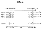
- FIG.2 is a schematic view showing a configuration of an optical switch module according to first embodiment of the present invention.
- This optical switch module comprises an incident side optical waveguide portion 101, a collimate portion 102, an incident side optical deflecting element portion 103, a common optical waveguide 104, an outgoing side optical deflecting element portion 105, a converging portion 106, and an outgoing side optical waveguide portion 107.
- the incident side optical waveguide portion 101, the collimate portion 102, the incident side optical deflecting element portion 103, the common optical waveguide 104, the outgoing side optical deflecting element portion 105, the converging portion 106, and the outgoing side optical waveguide portion 107 are formed integrally on the substrate.
- the incident side optical waveguide portion 101 consists of a plurality of optical waveguides (cores) 101a, and a cladding layer 101b that covers these optical waveguides 101a to confine the light in the optical waveguides 101a due to difference in the refractive index.
- the outgoing side optical waveguide portion 107 consists of a plurality of optical waveguides (cores) 107a, and a cladding layer 107b that covers these optical waveguides 107a to confine the light in the optical waveguides 107a due to difference in the refractive index.
- the number of the optical waveguides 101a of the incident side optical waveguide portion 101 is set equal to that of the optical waveguides 107a of the outgoing side optical waveguide portion 107.
- the collimate portion 102 consists of n collimate lenses 102a. Each collimate lens 102a is arranged at the position that is slightly remote from the end portion of the optical waveguide 101a. The light emitted from the optical waveguide 101a is spread radially and then is shaped into a parallel light by the collimate lens 102a.
- N optical deflecting elements 103a are provided to the incident side optical deflecting element portion 103.
- Each optical deflecting element 103a is arranged at the position that is slightly remote from the collimate lens 102a in the optical axis direction.
- the detailed explanation of the optical deflecting element 103a will be given later, but the optical deflecting element 103a can change the propagation direction of the light signal by utilizing the Pockels effect (electrooptic effect).
- the common optical waveguide 104 consists of a slub waveguide. This common optical waveguide 104 transmits the light, which is passed through the incident side optical deflecting element portion 103, to the outgoing side optical deflecting element portion 105. Plural light signals are simultaneously passed through the common optical waveguide 104, but these light signals can be transmitted without the interference with other light signals since such light signals can straightly propagate in the predetermined direction in the common optical waveguide 104.
- Optical deflecting elements (n optical deflecting elements) 105a are provided to the outgoing side optical deflecting element portion 105. These optical deflecting elements 105a deflect the light, which is passed through the common optical waveguide 104 to reach the optical deflecting elements 105a, in the direction in parallel with the optical waveguides 107a.
- the optical deflecting elements 103a, 105a have basically the same structure.
- the converging portion 106 consists of n converging lenses 106a. These converging lenses 106a have an action to collimate the light, which is passed through the optical deflecting elements 105a, and guide it to the optical waveguides 107a.
- the collimating lens 102a constituting the collimate portion 102 is a two-dimensional lens that consists of two portions 102c, 102d having different refractive indexes.
- the portion 102c having the high refractive index (convex lens portion) is formed by the same material as the optical waveguides (core) 101a, 107a.
- the portion 102d having the low refractive index is formed by the material that can collimate the light by the difference in the refractive index between the portion 102c having the high refractive index and this portion 102d having the low refractive index.
- the converging lens 106a of the converging portion 106 also consists of the portion 106c having the high refractive index (convex lens portion) and the portion 106d having the low refractive index.
- the direction of the lens is opposite to that of the collimating lens 102a.
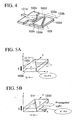
- the optical deflecting elements 103a constituting the incident side optical deflecting element portion 103 consist of one or plural prism pairs 103p.
- one prism pair 103p consists of a slab waveguide 103b formed by the material having the electrooptic effect, first and second upper electrodes 103c, 103d formed on the slab waveguide 103b, and first and second lower electrodes 103e, 103f formed under the slab waveguide 103b. All the first and second upper electrodes 103c, 103d and the first and second lower electrodes 103e, 103f are formed as a right- triangular shape (wedge shape).
- the first upper electrode 103c and the first lower electrode 103e are opposed mutually to put the slab waveguide 103b between them.
- the first upper electrode 103c and the second upper electrode 103d are positioned to make their oblique sides oppose mutually and are arranged closely.
- the second upper electrode 103d and the second lower electrode 103f are opposed mutually to put the slab waveguide 103b between them.
- the slab waveguide 103b is common to respective prism pairs 103p.
- the optical deflecting elements 105a of the outgoing side optical deflecting element portion 105 consist of the slab waveguide formed by the material having the electrooptic effect, and one or plural prism pairs 105p.
- Each prism pair 105p consists of a pair of first electrodes (the first upper electrode and the first lower electrode) and a pair of second electrodes (the second upper electrode and the second lower electrode).
- FIGS.5A and 5B are schematic views showing the deflection of light by the prism pair 103p.
- a white arrow indicates the direction of the crystal axis of the slab waveguide 103b
- a black arrow E indicates the direction of the electric field.
- the refractive index of the slab waveguide 103b between the first upper electrode 103c and the first lower electrode 103e is changed from n to n+ ⁇ n.
- the propagation direction of the light signal is deflected toward the left direction only by an angle ⁇ .
- the second upper electrode 103d is connected to the ground line (G) and the control voltage (+V) is applied to the second lower electrode 103f
- the refractive index of the slab waveguide 103b between the second upper electrode 103d and the second lower electrode 103f is changed from n to n- ⁇ n.
- the propagation direction of the light signal is further deflected toward the left direction only by an angle ⁇ .
- the electrodes to which the control voltage is applied are also referred to as the control electrode hereinafter.
- the light can be deflected by 2 ⁇ by using one prism pair.
- m is the integer of 2 or more
- prism pairs 103p are arranged in series every channel, the propagation direction of the light signal can be deflected by 2 ⁇ ⁇ m.
- the electrodes positioned to put the slab waveguide, that is formed by the material having the electrooptic effect, between them may be formed to directly contact to the slab waveguide (the core layer). In this case, if the cladding layer is interposed between these electrodes and the slab waveguide (the core layer), the optical loss caused by the propagation on the metal interface can be avoided.
- the first upper electrode 103c and the second upper electrode 103d are positioned to make their oblique sides oppose mutually and are arranged closely.
- the first lower electrode 103e and the second lower electrode 103f are positioned to make their oblique sides oppose mutually and are arranged closely. Therefore, the size of the prism pair 103p can be reduced.
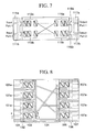
- FIG.7 shows an example in which the present invention is applied to the 2 ⁇ 2-channel optical switch module.
- the first light signal being input into an input port 1 is transmitted to any one of an output port 1 or an output port 2
- the second light signal being input into an input port 2 is transmitted to any one of the output port 1 or the output port 2.
- the light signal is not deflected by the optical deflecting elements 113a, 113b, 115a, 115b unless the voltage is applied to all the optical deflecting elements 113a, 113b, 115a, 115b.
- the light signal being input into the channel waveguide 111a is transmitted to the optical waveguide portion 117a and the light signal being input into the channel waveguide 111b is transmitted to the optical waveguide portion 117b respectively.
- the positive voltage V is applied to the control electrodes of the optical deflecting elements 113a, 115b and the negative voltage V is applied to the control electrodes of the optical deflecting elements 113b, 115a.
- the light signal being input into the input port 1 is deflected rightward by the optical deflecting element 113a to reach the optical deflecting element 115b, then is deflected by the optical deflecting element 115b in the direction in parallel with the optical waveguide 117b, then is converged by the converging lens 116b to enter into the optical waveguide 117b, and then is transmitted to the output port 2.
- the light signal being input into the input port 2 is deflected leftward by the optical deflecting element 113b to reach the optical deflecting element 115a, then is deflected by the optical deflecting element 115a in the direction in parallel with the optical waveguide 117a, and then is transmitted to the output port 1 via the converging lens 116a and the optical waveguide 117a.
- FIG.8 is a plan view of the 4 ⁇ 4-channel optical switch module.
- the same voltage is applied the control electrode of the optical deflecting element on the light signal outputting side and the control electrode of the optical deflecting element on the light signal receiving side.
- a large number of light signals are simultaneously passed through the common optical waveguide 104, but respective light signals never interfere with each other since the light signals linearly travel in the predetermined directions respectively in the common optical waveguide 104.
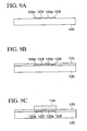
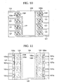
- FIGS.9A to 9F show a cross section taken along a I-I line in FIG.8.
- FIG.13 is a side view showing one input port.
- an Au (gold) film of about 2000 ⁇ thickness is formed on a silicon substrate 120 by the sputter method.
- the first and second lower electrodes 103e, 103f of the incident side optical deflecting element 103a, the first and second lower electrode 103e, 103f of the outgoing side optical deflecting element 105a, a signal line 121, and a ground line 122 are formed by patterning the Au film.
- the first lower electrodes 103e, 105e are connected commonly to the ground line 122
- the second lower electrodes 103f, 105f are connected individually to the signal line 121 every optical deflecting element.
- the shape of the first and second lower electrodes 103e, 105e, 103f, 105f are the right triangle, for example, and the length of the optical beam in the width direction is set to 200 to 500 ⁇ m, for example. Also, the first lower electrode 103e and the second lower electrode 103f are formed closely to make their oblique sides oppose mutually. Similarly, the first lower electrode 105e and the second lower electrode 105f are formed closely to make their oblique sides oppose mutually.
- the first and second lower electrodes 103e, 105e, 103f, 105f are covered with this lower cladding layer 123.
- the material of the lower cladding layer 123 is not limited to the above epoxy resin, and various materials can be employed.
- the fluorinated polyimide resin (OPI-N3205 (refractive index 1.52) manufactured by Hitachi Chemical Co., Ltd.) may be employed as the material of the lower cladding layer 123.
- an electrooptic thin film 124 serving as the slab waveguides 103b, 105b is formed in the optical deflecting element portions 103, 105.
- This electrooptic thin film 124 is formed by coating the organic nonlinear optical material such as paranitroaniline by a thickness of about 5 ⁇ m, for example.
- the material of the electrooptic thin film 124 PZT (Pb(Zr, Ti)O 3 ), PLZT ((Pb, La)(Zr, Ti)O 3 ), etc., for example, may be employed other than the above organic nonlinear optical material.
- the method of forming these electrooptic thin films there are the sputter method, the sol-gel method, the MOCVD (Metal Organic Chemical Vapor Deposition) method, etc.
- the formed optical crystal (electrooptic thin film) for example, is polished thin and then pasted onto the lower cladding layer 123.
- a resin film is formed by coating a resin, which has the refractive index higher than the lower cladding layer 123, (for example, a resin that contains bisphenyl A diglycidyl as the principal component to adjust the refractive index to 1.520) on the substrate 120.
- a resin which has the refractive index higher than the lower cladding layer 123, (for example, a resin that contains bisphenyl A diglycidyl as the principal component to adjust the refractive index to 1.520) on the substrate 120.
- the optical waveguides (cores) 101a, 107a, the collimate lens 102a, the converging lens 106a, and the common optical waveguide 104 are formed by patterning this resin film.
- the material of the optical waveguides (cores) 101a, 107a, the collimate lens 102a, the converging lens 106a, and the common optical waveguide 104 is not limited to the above epoxy resin and various materials may be employed.
- the fluorinated polyimide resin OPI-N3205 (refractive index 1.52) manufactured by Hitachi Chemical Co., Ltd.
- the fluorinated polyimide resin may be employed as the material of the optical waveguides (cores) 101a, 107a, the collimate lens 102a, the converging lens 106a, and the common optical waveguide 104.
- an upper cladding layer 125 is formed by using the same resin as the lower cladding layer 123 to have a thickness of 5 ⁇ m or less.
- a low refractive index resin is filled to bury the clearances of the high refractive index resin in the collimate portion 102 and the converging portion 106 (portions 102d, 106d in FIG.3).
- the clearances of the high refractive index resin may be filled with the air.
- the first upper electrodes 103c, 105c and the second upper electrodes 103d, 105d are formed on the upper cladding layer 125.
- the first upper electrodes 103c, 105c are connected to the individual signal lines 126 every optical deflecting element, and the second upper electrodes 103d, 105d are connected commonly to the ground line 127. In this manner, the optical switch module according to the first embodiment can be manufactured.
- the polymer is employed as the waveguide material.
- the inorganic material such as quartz is employed as the waveguide material, the optical loss can be further reduced.
- r is the electrooptic constant
- n is the refractive index
- E is the electric field strength.
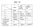
- FIG.14 shows values of the deflection angle ⁇ per one prism pair when LiNbO 3 , PZT, and PLZT are employed as the slab waveguide.
- the calculations are made theoretically under the assumptions that an angle ⁇ of a top end portion of the electrode is 45 degree, the refractive indexes of LiNbO 3 , PZT, and PLZT are 2.2, 2.4, and 2.4 respectively, the electrooptic constant r of LiNbO 3 is 30 pm/V, the electrooptic constant r of the PZT film formed by the sol-gel method is 50 pm/V, the electrooptic constant r of the PLZT sintered film is 612 pm/V, the electric field strength E applied to LiNbO 3 is 10 V/ ⁇ m, the electric field strength E applied to the PZT film formed by the sol-gel method is 100 V/ ⁇ m, and the electric field strength E applied to the PLZT sintered film is 8.2 V/ ⁇ m.
- the number of the prism pairs must be set to 63 or more to get the deflection angle of ⁇ 5 degree or more. In the case of PZT and PLZT, the number of the prism pairs must be set to 4 or more. Also, the optical loss is 1 dB/cm if LiNbO 3 is employed, the optical loss is 1.7 dB/cm if PZT is employed, and the optical loss is 0.7 dB/cm if PLZT is employed.
- the prism pairs of the optical deflecting element are formed by using PLZT and the beam diameter of the light that is passed through the collimate lens is assumed as 240 ⁇ m
- the light can be deflected in an angle range of 12.8 degree ( ⁇ 6.4 degree) if a size of the first prism pair is set to 300 ⁇ m, a size of the second prism pair is set to 334 ⁇ m, a size of the third prism pair is set to 408 ⁇ m, and a size of the fourth prism pair is set to 536 ⁇ m, as shown in FIG.15.
- the optical switch module As shown in FIG.16, if an optical waveguide pitch is 600 ⁇ m and the maximum deflection angle ⁇ max by the optical deflecting element is set to 10.7 degree (almost ⁇ 5.4 degree), a width of the slab waveguide is 19 mm and a length is 100 mm. An overall size of the optical switch module including the incident side optical waveguide, the outgoing side optical waveguide, the collimate lens and the converging lens is almost 140 ⁇ 40 mm. In this manner, according to the first embodiment, the optical switch module that is smaller in size than the prior art can be achieved.
- the incident side optical waveguides and the outgoing side optical waveguides are illustrated in parallel.
- all the incident side optical waveguides may be arranged such that they are slightly inclined mutually to the optical waveguides, that are arranged in the middle of the outgoing side optical waveguides, and also all the outgoing side optical waveguides may be arranged such that they are slightly inclined mutually to the optical waveguides, that are arranged in the middle of the incident side optical waveguides.
- the maximum deflection angle ⁇ max of each optical deflecting element can be set identically ( ⁇ 5.4 degree).
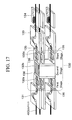
- FIG.17 is a schematic view showing a light signal switching device employing the above optical switch module
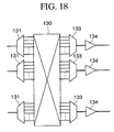
- FIG.18 is a block diagram showing the same.
- This light signal switching device receives the WDM signals, in which the light signals for 64 wavelengths are multiplied at 40 Gb/s, by 64 systems and then switches the propagation destination of these light signals.
- the light signal switching device comprises 32 AWG optical branching filters 131 arranged in the vertical direction, an optical switch module group 130, 32 optical multiplexers 133, and 32 optical amplifiers (EDFAs: Erbium- Doped Fiber Amplifiers) 134.
- the optical switch module group 130 is constructed in a three-stage fashion.
- the optical switch module group in the first stage is constructed by 32 32 ⁇ 64-channel optical switch module 132a that are aligned in the vertical direction
- the optical switch module group in the second stage is constructed by 64 32 ⁇ 32-channel optical switch module 132b that are aligned in the horizontal direction
- the optical switch module group in the third stage is constructed by 32 64 ⁇ 32-channel optical switch module 132c that are aligned in the vertical direction.
- the optical switch module group in the second stage is arranged in the state that it is rotated from the optical switch module groups in the first and third stages by 90 degree.
- the optical branching filters 131 and the optical switch module 132a in the first stage, the optical switch module 132a in the first stage and the optical switch module 132b in the second stage, the optical switch module 132b in the second stage and the optical switch module 132c in the third stage, and the optical switch module 132c in the third stage and the optical multiplexers 133 are connected via optical connectors 135, 136 respectively.
- the optical connector 136 consists of a substrate 140, and a large number of minute lenses 141 that'pass the light in the thickness direction of the substrate 140.
- lenses 141 are arranged in the two-dimensional direction in the optical connector 136, and the lenses 141 are arranged in the one- dimensional direction in the optical connector 135.
- an alignment pitch of the lenses 141 is set identically to an alignment pitch of the input/output ports of the optical switch module 132.
- the lenses 141 of these optical connectors 135, 136 act to converge the light, which is output from the optical devices in the preceding stage, and transmit the light to the optical devices in the succeeding stage, and are useful to reduce the transmission loss.
- the multiplied light signal is separated into individual light signals by the optical branching filter 131. Then, the propagation destinations of respective light signals are switched by the optical switch module group 130.
- the optical switch modules are constructed by the 32 32 ⁇ 64-channel optical switch module 132a, the 64 32 ⁇ 32-channel optical switch module 132b, and the 32 64 ⁇ 32-channel optical switch module 132c respectively, and the three-stage construction (cascade-connection) is built up by rotating three-set of optical switch module groups by 90 degree. Therefore, the light signal input into any input port can be output to any port of 1024 output ports.
- the light signals whose propagation destinations are switched by the light signal switching device are multiplexed by the optical multiplexer 133 every destination, and then amplified by optical amplifiers 134 to output.
- the loss can be reduced. Also, in contrast to the case that these optical devices are connected via the optical fibers, a connecting operation is extremely easy and also a size of the device can be reduced considerably.
- first and third optical switch modules 145, 147 may be constructed by arranging 128 optical switch modules 132 in 2 columns in the width direction and in 64 columns in the height direction.
- a second optical switch module 146 may be constructed by 128 64 ⁇ 64-channel optical switch modules 132, which are aligned in the direction that is rotated from the optical switch modules 132 of the first and third optical switch modules 145, 147 by 90 degree.
- FIG.21 is a schematic view showing an example of an optical connector 155 when the 32-system light signal, in which the light signal having 128 wavelengths is multiplied from the optical branch filter 150, is input into an optical switch module group 160 having the input ports that are arranged in 64 rows and 64 columns.
- This optical connector 155 consists of an interlayer shifting portion 155a that transmits the light signal from the optical waveguide layer on one surface side of the substrate to the optical waveguide layer on the other surface side or from the optical waveguide layer on the substrate to the optical waveguide layer on other substrate, and an interlayer bending portion 155b that changes the traveling direction of light in the same optical waveguide layer.
- the interlayer shifting portion 155a the even-numbered light signals out of the 128 light signals, that are branched by the optical branching filter, are shifted to the direction perpendicular to the substrate surface by using the reflection mirror shown in FIG.22A. Then, the interlayer bending portion 155b, the position of the output side optical waveguides are aligned to coincide with the input ports of the optical switch module group by bending the traveling direction of the light signal within the plane that is parallel with the substrate by virtue of the reflection mirror shown in FIG.22B.
- the light signals can be input in the input ports of the optical switch module respectively.
- the deflection angle of the light signal is controlled by changing the voltage applied to the control electrodes of respective prism pairs.
- the deflection angle of the light signal may be controlled by changing the number of the prism pairs to which the control voltage is applied while keeping the control voltage constant.
- FIG.23 is a top view showing an optical wiring substrate according to a second embodiment of the present invention.
- an optical wiring substrate in which a dielectric multi-layered film mirror 212 is arranged at a bending portion of an optical waveguide 211, which is bent at a right angle will be explained hereunder.
- the dielectric multi-layered film mirror 212 is arranged at the bending portion of the optical waveguide 211 to have an angle of 45 degree to the center line (indicated by a dot-dash line in FIG.23) of the optical waveguide 211.
- This dielectric multi-layered film mirror 212 is formed by providing a plurality of mutually-parallel slits 205 in a part of the optical waveguide 211.
- this dielectric multi-layered film mirror 212 is constructed by forming a part of the optical waveguide 211 as the high refractive- index layer of the dielectric multi-layered film mirror 212 and using the air in the slits 205 as the low refractive-index layer of the dielectric multi-layered film mirror 212.
- the interface between the first high refractive- index layer and the low refractive-index layer of the dielectric multi-layered film mirror 212 is arranged on the front side rather than the theoretical reflection surface (indicated by a chain double-dashed line in FIG.23) in which the intersection point of the center lines of the optical waveguide 211 is contained. That is, in the optical wiring substrate of the second embodiment, the theoretical reflection surface is contained in the dielectric multi-layered film mirror 212.
- FIG.24 is a schematic view showing an effect of the optical wiring substrate of the second embodiment.
- the light can be totally reflected at the interface between the first high refractive-index layer and the low refractive-index layer of the dielectric multi-layered film mirror 212 if the refractive index of the high refractive-index layer is more than 1.41 and also the light propagates in parallel with the center line of the optical waveguide (core) 211, so that there is no necessary that the dielectric multi-layered film mirror 212 should be formed as the multi-layered structure.
- the interface 211c between the optical waveguide 211 and the air (cladding layer) as the reflection mirror.
- the light indicated by an arrow c in FIG.24
- the lights indicated by arrows a, b, d in FIG.24
- the peripheral low refractive- index layer the air in the second embodiment
- the layer structure of the dielectric multi-layered film mirror 212 should be optimized for the light that is incident upon the dielectric multi-layered film mirror 212 at an angle (( ⁇ 1+ ⁇ 2)/2) obtained by bisecting a sum of an angle ⁇ 1 of the light beam L1 and an angle ⁇ 2 of the light beam L2.
- this light beam L1 has the critical angle to the interface between the first low refractive-index layer and the high refractive-index layer of the dielectric multi-layered film mirror 212
- this light beam L2 of the light that propagates while reflecting on the wall surface of the optical waveguide 211, has the smallest angle to the normal (indicated by a chain double-dashed line in FIG.25) of the dielectric multi-layered film mirror 212.
- the periodic structure is set such that the plane which is parallel with the reflection plane of the dielectric multi-layered film mirror 212 and contains the intersection point of the center lines of the bending portion of the optical waveguide can be contained in the dielectric multilayered film mirror 212, whereby the lights that are out of the total reflection conditions can be returned to the inside of the optical waveguide at the reflection plane of the optical waveguide.
- the loss can be reduced in the bending portion of the optical waveguide.
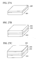
- FIGS.27A to 27F are perspective views showing a method of manufacturing the optical wiring substrate according to the second embodiment.
- a lower cladding layer 202 is formed on a silicon substrate 201 by spin-coating the resin that has the low refractive index, e.g., fluorinated polyimide resin OPI-N3205 (manufactured by Hitachi Chemical Co., Ltd.) whose refractive index is 1.52, to have a thickness of about 5 to 10 ⁇ m and then curing the resin by the heating.
- the resin that has the low refractive index e.g., fluorinated polyimide resin OPI-N3205 (manufactured by Hitachi Chemical Co., Ltd.) whose refractive index is 1.52
- a core layer 203 is formed by spin-coating the resin that has the refractive index higher than the lower cladding layer 202, e.g., fluorinated polyimide resin OPI-N3405 (manufactured by Hitachi Chemical Co., Ltd.) whose refractive index is 1.53, to have a thickness of about 10 ⁇ m and then curing the resin by the heating.
- the resin that has the refractive index higher than the lower cladding layer 202, e.g., fluorinated polyimide resin OPI-N3405 (manufactured by Hitachi Chemical Co., Ltd.) whose refractive index is 1.53, to have a thickness of about 10 ⁇ m and then curing the resin by the heating.
- a photoresist film 204 is formed by coating photoresist on the core layer 203.
- the photoresist that can be exposed by the ultraviolet rays and the electron beam and that has the resistance to the dry etching by using the oxygen plasma is employed.
- the electron beam is irradiated onto the portion of the photoresist film 204, in which the low refractive-index layer (slits) of the dielectric multilayered film mirror 212 are formed, to expose there.
- patterns of the low refractive-index layer are drawn such that the plane which is parallel with the reflection plane of the dielectric multi-layered film mirror 212 and contains the intersection point of the center lines of the optical waveguide 211 can be contained in the inside of the dielectric multilayered film mirror 212.
- the optical waveguide 211 is formed of the fluorinated polyimide resin whose refractive index is 1.53
- a thickness of the high refractive-index layer must be set to about 0.15 ⁇ m
- a thickness of the low refractive-index layer (a width of the slit 205) must be set to about 0.19 ⁇ m
- the number of the low refractive-index layer must be set to three layers or more.
- the optical waveguide forming regions (containing the dielectric multi-layered film mirror forming regions) of the photoresist film 204 are masked and other portions are exposed by the ultraviolet rays (UV). Then, the photoresist film 204 is patterned as shown in FIG.27D by executing the developing process.
- an optical waveguide 211 is formed by dry-etching the core layer 203 by means of the oxygen plasma (300 W) while using the photoresist film 204 remaining on the core layer 203 as a mask.
- the etching is continued until a lower end of the slit 205 serving as the low refractive-index layer of the dielectric multi-layered film mirror 212 reaches the lower cladding layer 202.
- the photoresist film 204 is removed. In this manner, the optical wiring substrate of the second embodiment can be completed.
- the dielectric multi-layered film mirror 212 is constructed by forming a plurality of slits 205 on the optical waveguide 211, the mirror having the reflection plane perpendicular to the substrate 201 can be easily fabricated. Also, since the plane that is parallel with the reflection plane of the dielectric multi-layered film mirror 212 and contains the intersection point of the center lines of the optical waveguide 211 is positioned in the inside of the dielectric multilayered film mirror 212, it is possible to manufacture the optical wiring substrate that has the small loss in the bending portion of the optical waveguide 211.
- the optical waveguide 211 is surrounded by the air.
- an upper cladding layer 213 may be formed by coating the optical waveguide 211 with the material whose refractive index is lower than the optical waveguide (core) 211 (e.g., epoxy resin).
- the same low refractive-index material as the upper cladding layer 213 should be filled into the inside of the slits 205 that are formed as the low refractive-index layer of the dielectric multi-layered film mirror 212, as described above.
- such filling of the low refractive-index material into the slits 205 should be carried out in vacuum not to remain the air in the slits 205.
- a reflection efficiency of the dielectric multi- layered film mirror 212 becomes higher as the refractive- index of the low refractive-index material filled into the slits 205 becomes lower.
- the same material as the above lower cladding layer 202 may be employed.
- the material having the lower refractive index e.g., fluorinated resin Cytop CTL-813A (refractive index 1.34: manufactured by ASAHI GLASS CO., LTD), should be employed.
- the optical waveguide (core) 211 having the slits 205 is formed, and then the fluorinated resin Cytop CTL-813A is coated on the substrate 201 in vacuum by the spin-coating method and then cured by the heating for one hour at the temperature of 180 °C.
- the optical wiring substrate in which the periphery of the optical waveguide (core) 211 is surrounded by the low refractive-index resin (upper cladding layer) can be manufactured.
- the layer number of the low refractive-index layer (slits 205) of the dielectric multi-layered film mirror 212 must be set to 20 or more.
- FIG.30 A variation of the second embodiment is shown in FIG.30.
- the light is multiply-reflected by respective layers of the dielectric multi-layered film. It will be lost if such light does not enter in the inside of the optical waveguide. Therefore, as shown in FIG.30, if the slits 205 are formed in the overall bending portion of the optical waveguide 211, the loss in the dielectric multi-layered film mirror 212 can be suppressed to the lowest minimum.
- FIG.31A is a plan view showing a structure of an optical deflecting element according to a third embodiment of the present invention
- FIG.31B is a sectional view showing the same.
- a lower electrode (first electrode) 301 made of conductive material such as the metal is formed on a single crystal substrate 300, and an optical waveguide 302 that is constructed by the crystal having the electrooptic effect is arranged on the lower electrode 301.
- the optical waveguide 302 has such a structure that a core layer 302a is put between upper and lower cladding layers 302b to confine the light in the core layer 302a due to the difference in the refractive index between the core layer 302a and the cladding layers 302b.
- the optical waveguide 302 may have the structure in which the light can be confined in the center portion of the optical waveguide 302 by changing the refractive index continuously.
- the core layer 302a of the optical waveguide 302 must be formed of the crystal having the electrooptic effect, but the cladding layers 302b do not always need the electrooptic effect.
- An upper electrode (second electrode) 303 and a leading electrode 305 are formed on the optical waveguide 302.
- the upper electrode 303 is formed as a wedge shape (right triangular shape) having a side that intersects orthogonally with the optical axis of the incident light (base) and a side that intersects obliquely with the optical axis (oblique side).
- the leading electrode 305 is connected electrically to the lower electrode 301 via a conductive film 304 on a side surface of the optical deflecting element.
- the light comes into the optical waveguide 302 from the base side of the upper electrode 303 and then goes out from the oblique side. If the voltage is applied between the upper electrode 303 and the leading electrode 305, the refractive index of the portion of the optical waveguide 302 under the upper electrode 303 is changed to cause the difference in the refractive index between such portion and the periphery.
- the light passing through the optical waveguide 302 is deflected at the portion whose refractive index is changed and the traveling direction of light is changed. That is, the outgoing direction of light can be controlled by changing the voltage that is applied between the upper electrode 303 and the leading electrode 305.
- the optical deflecting element of the third embodiment since the lower electrode 301 is formed on the single crystal substrate 300 and the optical waveguide 302 is formed on the lower electrode 301, the conductivity or semi-conductivity is not required for the single crystal substrate 300. Therefore, the manufacture of the substrate 300 becomes easy and also the production cost can be reduced.
- the optical deflecting element of the third embodiment since the leading electrode 305 electrically connected to the lower electrode 301 is arranged on the plane on which the upper electrode 303 is arranged, the mounting of the element onto other substrate (optical switch module substrate) can be made easy. In other words, when the optical deflecting element is to be mounted onto the optical switch module substrate, only the connection of the upper electrode 303 and the leading electrode 305 to the optical switch module substrate by the solder, etc. is required. Thus, the step of electrically connecting the lower electrode and the optical switch module substrate after the optical deflecting element is mounted onto the optical switch module substrate can be eliminated.
- FIGS.33A to 33D are sectional views showing a method of manufacturing the optical deflecting element according to the third embodiment in order of steps.
- the substrate suitable for the PZT crystal growth should be selected as the substrate 300.
- STO SiO 3
- the substrate 300 since the crystal constant is close to PZT.
- the lower electrode 301 of about 2000 ⁇ is formed by epitaxially growing SRO (SrRuO 3 ) or Pt (platinum) on the STO single crystal substrate 300 by the well-known film forming method such as the sol-gel method, the PLD (Pulsed Laser Deposition) method, the sputter method, the CVD method, or the like.
- the thickness of the lower electrode 301 is below 1000 ⁇ is not preferable since the resistance value is increased.
- the resistance value can be reduced if the thickness of the lower electrode 301 is increased, but the crystallinity of the optical waveguide 302 formed on the lower electrode 301 is degraded. For this reason, it is preferable that, as described above, the thickness of the lower electrode 301 should be set to about 2000 ⁇ .
- the optical waveguide 302 is formed on the lower electrode 301 by epitaxially growing PLZT (cladding layer)/PZT (core layer)/PLZT (cladding layer) sequentially.
- a thickness of the optical waveguide 302 is set to almost 1 to 10 ⁇ m, for example.
- side surfaces (the light incident plane, the light outgoing plane, and other planes) of the structure consisting of the substrate 300, the lower electrode 301, and the optical waveguide 302 are polished to planarize sufficiently and to expose the lower electrode 301 from the side surface.
- the conductive film 304 having a thickness of about 2000 ⁇ or more is formed by depositing Pt on one side surface (except the light incident plane and the light outgoing plane) of the structure by virtue of the sputter method, etc., for example.
- the lower electrode 301 is connected electrically to this conductive film 304 via the portion exposed from the side surface.
- the conductive film made of Pt, or the like and having a thickness of about 2000 ⁇ or more is formed on the optical waveguide 302 by virtue of the sputter method, etc., for example.
- the upper electrode 303 of the wedge shape (right triangular shape) and the leading electrode 305, which is connected electrically to the lower electrode 301 via the conductive film 304, are formed by patterning this conductive film by virtue of the photolithography method.
- the optical deflecting element of the third embodiment can be completed.
- the substrate 300 since the lower electrode 301 is formed on the substrate 300, it is not needed that the substrate 300 is conductive. Therefore, the substrate that is suitable for the formation of the optical waveguide 302 can be selected as the substrate 300 regardless of the conductivity. As a result, the optical deflecting element that is excellent in the crystallinity, has the small optical loss, and has good optical properties can be obtained.
- the optical deflecting element of the third embodiment employs the conductive material such as the metal having the small electric resistance as the lower electrode 301, it is possible to execute the high-speed operation.
- the optical deflecting element of the third embodiment can be easily mounted on other substrate.
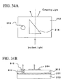
- FIG.34A is a plan view showing a structure of an optical deflecting element according to a fourth embodiment of the present invention
- FIG.34B is a sectional view showing the same.
- a lower electrode 311 made of conductive material such as the metal is formed on a single crystal substrate 310, and an optical waveguide 312 having a laminated structure of cladding layer/core layer/cladding layer, as shown in FIG.32, for example, is formed on this lower electrode 311.
- an upper electrode 314 of the wedge shape (right triangular shape) having the side that intersects orthogonally with the optical axis of the incident light (base) and the side that intersects obliquely with the optical axis (oblique side) and a circular leading electrode 315 are formed on the optical waveguide 312.
- the leading electrode 315 is connected electrically to the lower electrode 311 via the column-like conductor 313 that pass through vertically the optical waveguide 312.
- the light enters into the optical waveguide from the base side of the upper electrode 314 and then goes out from the oblique side. If the voltage is applied between the upper electrode 314 and the leading electrode 315, the refractive index of the portion of the optical waveguide 312 under the upper electrode 314 is changed to cause the difference in the refractive index between the portion and the periphery.
- the light passing through the optical waveguide 312 is deflected at the portion whose refractive index is changed and the traveling direction of light is changed. That is, the outgoing direction of light can be controlled by changing the voltage that is applied between the upper electrode 314 and the leading electrode 315.
- FIGS.35A to 35E are sectional views showing a method of manufacturing the optical deflecting element according to the fourth embodiment in order of steps.
- the lower electrode 311 of about 2000 ⁇ thickness is formed on the STO single crystal substrate 310 by epitaxially growing SRO or Pt.
- a Cu (copper) film for example, is formed on the lower electrode 311 by the sputter method.
- the column-like conductor 313 is formed by patterning the Cu film by virtue of the photoresist method.
- a height of this column-like conductor 313 (height of the Cu film) must be set to exceed the thickness of the optical waveguide 312 that is formed subsequently.
- the optical waveguide 312 of about 1 to 10 ⁇ m thickness is formed by epitaxially growing PLZT (cladding layer)/PZT (core layer)/PLZT (cladding layer) sequentially on the lower electrode 311.
- PLZT cladding layer
- PZT core layer
- PLA PLZT
- a surface of the optical waveguide 312 is polished to planarize and to expose the column-like conductor 313.
- the conductive film of about 2000 ⁇ thickness is formed on the optical waveguide 312 by depositing Pt, for example.
- the upper electrode 314 of the wedge shape and the leading electrode 315 which is connected electrically to the lower electrode 311 via the column-like conductor 313, are formed by patterning this conductive film by virtue of the photolithography method.
- the optical deflecting element of the fourth embodiment can be completed.
- the optical deflecting element of the fourth embodiment has such an advantage that the mass productivity is excellent, in addition to the same advantages of the third embodiment. That is, if the optical deflecting elements as shown in FIGS.31A and 31B and FIGS.34A and 34B are manufactured, it may be considered that a number of optical deflecting elements are formed simultaneously on a sheet of substrate and then individual optical deflecting elements are obtained by dividing the substrate near the final step. However, in the optical deflecting element shown in FIGS.31A and 31B, for convenience of the electrical connection between the lower electrode 301 and the leading electrode 305 via the conductive film 304 formed on the side surface, the conductive film 304 cannot be formed even after the substrate is divided.
- the optical deflecting element of the fourth embodiment the column-like conductor 313 for connecting the lower electrode 311 and the leading electrode 315 is formed by forming the Cu film on the overall upper surface of the lower electrode 311 and then patterning this Cu film by the photolithography method. Therefore, the column-like conductor 313 can be formed before the substrate is divided, and thus the production efficiency can be increased.
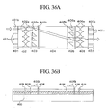
- FIG.36A is a plan view showing an optical switch module according to a fifth embodiment of the present invention
- FIG.36B is a sectional view showing the same.
- This optical switch module is constructed by an incident side optical waveguide portion 401, a collimate portion 402, an incident side optical deflecting element portion 403, a common optical waveguide 404, an outgoing side optical deflecting element portion 405, a converging portion 406, and an outgoing side optical waveguide portion 407.
- the incident side optical waveguide portion 401, the collimate portion 402, the common optical waveguide 404, the converging portion 406, and the outgoing side optical waveguide portion 407 are formed integrally on the optical switch module substrate (first substrate) 400.
- optical deflecting element portion 403 and the outgoing side optical deflecting element portion 405 optical deflecting element units 403b, 405b that are formed separately from the incident side optical waveguide portion 401, the collimate portion 402, the common optical waveguide 404, the converging portion 406, and the outgoing side optical waveguide portion 407 are jointed to the optical switch module substrate 400.
- a refracting medium e.g., resin
- the medium having the intermediate refractive index between the refractive index of the core layer of the collimate portion 402, the common optical waveguide 404, and the converging portion 406 and the refractive index of the core layer of the optical deflecting element units 403b, 405b is employed.
- the reflection preventing film having the multi-layered structure can be formed on the end surfaces of the optical deflecting element units 403b, 405b to overcome such large optical loss.
- the reflection preventing film is employed in various optical parts, and thus its explanation will be omitted herein because such reflection preventing film belongs to the well-known technology.
- the incident side optical waveguide portion 401 comprises four optical waveguides (cores) 401a, and a cladding layer 401b for covering these optical waveguides 401a to confine the light in the optical waveguides 401a because of the difference in the refractive index.
- the outgoing side optical waveguide portion 407 comprises four optical waveguides (cores) 407a, and a cladding layer 407b for covering these optical waveguides 407a to confine the light in the optical waveguides 407a because of the difference in the refractive index.
- the collimate portion 402 consists of four sets of collimate lens groups, and each collimate lens group is composed of a pair of convex lenses 402a.
- This convex lens 402a is a two-dimensional lens consisting of the core layer and cladding layers that sandwich the core layer vertically.
- a refracting medium 409 for adjusting the refractive index is filled between these convex lenses 402a.
- Each collimate lens group is arranged at the position to respond to the optical waveguide 401a respectively.
- the incident side optical deflecting element unit 403b consists of four optical deflecting elements 403a that are formed integrally on the same substrate (second substrate). These optical deflecting elements 403a have basically the same structure as the optical deflecting element in the third or fourth embodiment.
- the outgoing side optical deflecting element unit 405b consists of four optical deflecting elements 405a that are formed integrally on the same substrate (second substrate). These optical deflecting elements 405a have basically the same structure as the optical deflecting element in the third or fourth embodiment.
- the common optical waveguide 404 is composed of the slab waveguide.
- the light that is passed through the incident side optical deflecting element portion 403 travels straightly in the common optical waveguide 404, and reaches the outgoing side optical deflecting element portion 405.
- the converging portion 406 consists of four sets of converging lens groups, and each converging lens group is composed of a pair of convex lenses 406a.
- This convex lens 406a is a two-dimensional lens consisting of the core layer and cladding layers that sandwich the core layer vertically.
- the refracting medium 409 for adjusting the refractive index is filled between these convex lenses 406a.
- Each converging lens group is arranged at the position to respond to the optical deflecting element 405a respectively.
- FIGS.37A and 37B are schematic sectional views showing a method of connecting the optical deflecting element unit 403b and the optical switch module substrate 400.
- a substrate 410 of the optical deflecting element unit 403b is illustrated on the upper side and an upper electrode 414 thereof is illustrated on the lower side.
- a lower electrode 411 made of conductive material such as the metal is formed on a surface of the substrate 410 (the lower side in FIGS.37A and 37B) of the optical deflecting element unit 403b, while an optical waveguide 412 consisting of a core layer and a cladding layer is formed on a surface of the lower electrode 411 (the lower side in FIGS.37A and 37B).
- a wedge-shaped (right triangular shape) upper electrode 414, a leading electrode 415 connected to the lower electrode 411 via a column-like conductor 413 that passes through the optical waveguide 412, and a dummy electrode 416 are formed on a surface of the optical waveguide 412 (the lower side in FIGS.37A and 37B).
- the dummy electrode 416 is provided to connect horizontally and firmly the optical deflecting element portion 403 to the optical switch module substrate 400. No electric signal is supplied to the dummy electrode 416.
- a copper thin film should be formed on surfaces of these electrodes 414, 415, 416 with regard to the joinability to the solder.
- electrodes 420 are formed at positions, which coincide with the upper electrode 414, the leading electrode 415, and the dummy electrode 416 of the optical deflecting element 403a respectively, on the optical switch module substrate 400.
- the electrodes 420 connected to the upper electrode 414 and the leading electrode 415 are connected to a wiring (not shown) to which a signal of driving the optical deflecting element 403a is supplied.
- the optical deflecting element unit 403b can be mounted on the substrate 400 by using the apparatus such as the flip-chip bonder, or the like, which is normally employed to mount the semiconductor device (IC: Integrated Circuit).
- the optical deflecting element unit 403b can be mounted on the substrate 400 by jointing the electrodes 420 on the substrate 400 to the electrodes 414, 415, 416 on the optical deflecting element unit 403b by the solder 421, while directing the surface on which the upper electrode 414, the leading electrode 415, and the dummy electrode 416 are formed to the optical switch module substrate 400. Therefore, the electric connection between the optical deflecting element unit 403b and the substrate 400 can be executed at the same time. Similarly to this, the outgoing side optical deflecting element unit 405b can be mounted onto the optical switch module substrate 400.
- the positions of the core layers of the optical waveguides of the optical deflecting element units 403b, 405b and the positions of the core layers of the collimate portion 402, the common optical waveguide 404, and the converging portion 406 must be set to coincide mutually.
- the thicknesses of the core layer and the cladding layer of the optical deflecting element units 403b, 405b must be managed precisely.
- the light that enters into any one optical waveguide 401a of the incident side optical waveguide portion 401 travels in the optical waveguide 401a while reflecting on the interface between the core layer and the cladding layer, and then is emitted from the end portion of the optical waveguide 401a to spread radially.
- This light is shaped into the parallel light by the collimate portion 402, and then deflected into a predetermined direction in response to the applied voltage by the optical deflecting element 403a.
- the light that is output from the optical deflecting element 403a travels straightly in the common optical waveguide 404 to reach any one optical deflecting element 405a of the outgoing side optical deflecting element portion 405, and then is refracted in response to the applied voltage by the optical deflecting element 405a.
- the light that is refracted by the optical deflecting element 405a is converged by the converging portion 406 to enter into the outgoing side optical waveguide 407a, and then is emitted from the end portion of the optical waveguide 407a to the outside.
- the voltage applied to the incident side optical deflecting element 403a and the outgoing side optical deflecting element 405a a is adjusted, the light that is input into any optical waveguide of four incident side optical waveguides 401a can be transmitted to any optical waveguide of four outgoing side optical waveguides 407a.
- the optical deflecting element units 403b, 405b must be fabricated by the material with the electrooptic effect, so that the incident side optical waveguide portion 401, the collimate portion 402, the common optical waveguide 404, the converging portion 406, and the outgoing side optical waveguide portion 407 can be fabricated by the material having no electrooptic effect.
- the crystal material with the electrooptic effect is employed. Therefore, it is not preferable to form the overall optical switch module by the crystal material with the electrooptic effect.
- the optical deflecting element units 403b, 405b must be formed by the crystal material having the electrooptic effect, and other portions can be formed by the crystal material having the small optical loss. As a result, the optical switch module having the small optical loss can be obtained.
- the optical deflecting element units 403b, 405b can be connected firmly.
- the optical deflecting element units 403b, 405b can be jointed in the situation that they are maintained in parallel with the surface of the substrate 400.
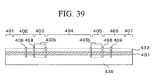
- FIG.38 is plan view showing an optical switch module according to a variation of the fifth embodiment of the present invention.
- the same symbols are affixed to the same elements as those in FIG.36A, and therefore their detailed explanation will be omitted.
- eight sets of incident side optical waveguides 401a, the collimate portion 402 consisting of eight sets of collimate lens groups, the converging portion 406 consisting of eight sets of converging lens groups, and eight sets of outgoing side optical waveguides 407a are formed on the substrate 400.
- two optical deflecting element units 403b in which four optical deflecting elements 403a are formed integrally are arranged in parallel in the incident side optical deflecting element portion 403.
- two optical deflecting element units 405b in which four optical deflecting elements 405a are formed integrally are arranged in parallel in the outgoing side optical deflecting element portion 405.
- the optical deflecting elements are needed in number in conformity with the scale of the optical switch module in the incident side optical deflecting element portion and the outgoing side optical deflecting element portion. If it is tried to form these optical deflecting elements on one substrate, the yield of the optical switch module is lowered because of the defect or the bowing of the optical deflecting element unit.
- the optical deflecting element units 403b, 405b are constructed by several (four in this example) optical deflecting elements respectively, and also the optical deflecting element units 403b, 405b are arranged in plural in parallel respectively.
- the reduction in the yield can be avoided.
- the optical deflecting element portions 403, 405 are divided into plural optical deflecting element units 403b, 405b, the number of the common electrodes formed on the optical switch module substrate is increased. However, since these common electrodes can be connected mutually on the optical switch module substrate, the number of the wirings that are to be extended to the outside of the optical switch module substrate is not changed.
- the common optical waveguide 404 cannot be divided, but the incident side optical waveguide portion 401, the collimate portion 402, the converging portion 406, and the outgoing side optical waveguide portion 407 may be formed to be divided into plural units.
- FIG.39 is a sectional view showing an optical switch module according to a sixth embodiment of the present invention.
- the sixth embodiment shows an example in which the elements except for the optical deflecting element units are formed by the same material by using the silica waveguide technology.
- a quartz substrate 430 is prepared.
- This silica substrate 430 serves as the lower cladding layer of the optical waveguide.
- a core layer 431 and an upper cladding layer 432 are formed on the silica substrate 430 by the well-known PLC (Planar Lightwave Circuit) technology.
- the recesses that have a predetermined shape respectively are formed by etching the collimate portion 402, the incident side optical deflecting element portion 403, the outgoing side optical deflecting element portion 405, and the converging portion 406.
- the optical deflecting element units 403b, 405b are mounted onto the incident side optical deflecting element portion 403 and the outgoing side optical deflecting element portion 405 respectively, and the refracting medium 408 is filled into the clearances of the incident side optical deflecting element portion 403 and the clearances of the outgoing side optical deflecting element portion 405. Also, the refracting medium 409 is filled into the recesses of the collimate portion 402 and the converging portion 406.
- the optical switch module of the sixth embodiment can be formed.
Landscapes
- Physics & Mathematics (AREA)
- Nonlinear Science (AREA)
- General Physics & Mathematics (AREA)
- Optics & Photonics (AREA)
- Engineering & Computer Science (AREA)
- Microelectronics & Electronic Packaging (AREA)
- Optical Modulation, Optical Deflection, Nonlinear Optics, Optical Demodulation, Optical Logic Elements (AREA)
- Optical Integrated Circuits (AREA)
Abstract
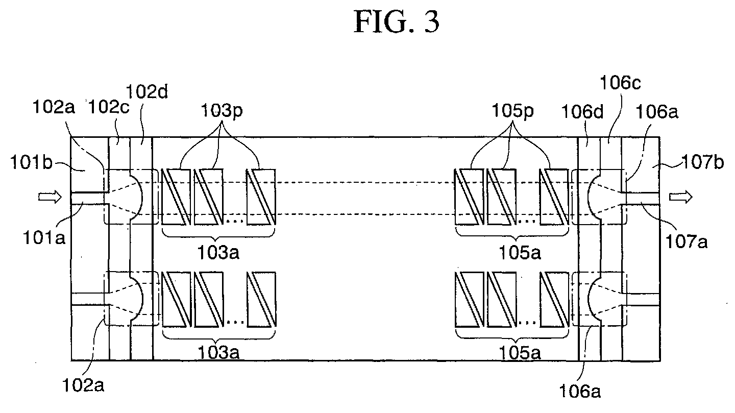
Description
Claims (31)
- An optical switch module comprising:wherein each of the first optical deflecting elements (103a) and the second optical deflecting elements (105a) is constructed by one or plural prism pairs, and each of the prism pairs includes a slab waveguide (103b) formed of material having the electrooptic effect, first and second upper electrodes (103c, 103d) formed as a wedge shape and arranged on a light signal passing area of the slab waveguide (103b) such that wedge top ends are directed mutually oppositely, and first and second lower electrodes (103e, 103f) arranged under the slab waveguide (103b) so as to oppose to the first and second upper electrodes (103c, 103d).a collimate portion (102) for collimating individually a plurality of light signals respectively;a plurality of first optical deflecting elements (103a) for switching propagation directions of the light signals, which are passed through the collimate portion (102), individually respectively by utilizing an electrooptic effect;a common optical waveguide (104) through which the light signals, which are passed through the plurality of first optical deflecting elements (103a) respectively, are propagated;a plurality of second optical deflecting elements (105a) for switching the propagation directions of the light signals, which are passed through the common optical waveguide (104), individually respectively by utilizing the electrooptic effect; anda converging portion (106) for converging the light signals, which are passed through the plurality of second optical deflecting elements (105a), individually respectively;
- An optical switch module according to claim 1, wherein a first potential is applied commonly to the first upper electrodes (103c) and the second lower electrodes (103f) of the prism pairs (103p), and a second potential is applied commonly to the second upper electrodes (103d) the first lower electrodes (103e).
- An optical switch module according to claim 1 or 2, wherein the collimate portion (102), the first optical deflecting elements (103a), the common optical waveguide (104), the second optical deflecting elements (105a), and the converging portion (106) are formed integrally.
- An optical switch module according to claim 1, 2 or 3, wherein a light propagation path is switched by causing the first optical deflecting elements (103a) and the second optical deflecting elements (105a) to cooperate with each other.
- A light signal switching device comprising:wherein each of the first, second and third optical switch module (132a,132b and 132c) includes (1) a collimate portion for collimating individually a plurality of light signals respectively, (2) a plurality of first optical deflecting elements for switching propagation directions of the light signals, which are passed through the collimate portion, individually respectively by utilizing an electrooptic effect, (3) a common optical waveguide through which the light signals, which are passed through the plurality of first optical deflecting elements respectively, are propagated, (4) a plurality of second optical deflecting elements for switching the propagation directions of the light signals, which are passed through the common optical waveguide, individually respectively by utilizing the electrooptic effect, and (5) a converging portion for converging the light signals, which are passed through the plurality of second optical deflecting element, individually respectively, anda first optical switch module group constructed by arranging a plurality of first optical switch modules (132a);a second optical switch module group constructed by arranging a plurality of second optical switch modules (132b) and connected optically to the first optical switch module group; anda third optical switch module group constructed by arranging a plurality of third optical switch modules (132c) and connected optically to the second optical switch module group;
wherein each of the first and second optical deflecting elements is constructed by one or plural prism pairs, and each of the prism pairs includes a slab waveguide formed of material having the electrooptic effect, first and second upper electrodes formed as a wedge shape and arranged on a light signal passing area of the slab waveguide such that wedge top ends are directed mutually oppositely, and first and second lower electrodes arranged under the slab waveguide so as to oppose to the first and second upper electrode. - A light signal switching device according to claim 5, wherein the second optical switch module group (146) is arranged in a state that the second optical switch module group is rotated by 90 degree to the first optical switch module group (145) and the third optical switch module group (147).
- A light signal switching device according to claim 5 or 6, wherein each of the first, second and third optical switch module (132a, 132b and 132c) has 'n input ports (where n is an integer of 2 or more) and n output ports, and each of the first, second and third optical switch module groups consists of n optical switch modules.
- A light signal switching device according to claim 5, 6 or 7, wherein a first potential is applied commonly to the first upper electrodes (103c) and the second lower electrodes (103f) of the prism pairs (103p), and a second potential is applied commonly to the second upper electrodes (103d) and the first lower electrodes (103e).
- A light signal switching device according to any one of claims 5 to 8, wherein the first optical switch module group and the second optical switch module group and the second optical switch module group and the third optical switch module group are optically connected via optical connectors (136) having a plurality of lenses (141), which are aligned in a one-dimensional or two-dimensional direction, respectively.
- A light signal switching device according to any one of claims 5 to 9, wherein an optical branching filter (131) for distributing wavelength-multiplexed light signals every wavelength is connected to an input side of the first optical switch module group, and an optical multiplexer (133) is connected to an output side of the third optical switch module group.
- A light signal switching device according to claim 10, wherein an optical amplifier (134) is connected to an output side of the optical multiplexer (133).
- A light signal switching device according to claim 10 or 11, wherein at least one of the optical branching filter and the first optical switch module group and the third optical switch module group and the optical multiplexer is connected via an optical connector (155) that has an interlayer shift mirror (155a) for shifting a light between layers and an in-plane shift mirror (155b) for shifting the light in a plane.
- An optical wiring substrate comprising:an optical waveguide (211) having a bended shape; anda dielectric multi-layered film mirror (212) having a plurality of slits (205) provided to a bending portion of the optical waveguide (211) as a part of a multi-layered structure.
- An optical wiring substrate according to claim 13, wherein a plane that is parallel with a reflection plane of the dielectric multi-layered film mirror (212) and contains an intersection point of center lines of the optical waveguide (211) at the bending portion is contained in an inside of the dielectric multi-layered film mirror (212).
- An optical wiring substrate according to claim 13 or 14, wherein the slits (205) are formed to have a depth that extends from an upper surface to a lower surface of the optical waveguide (211).
- An optical wiring substrate according to claim 13, 14 or 15, wherein the dielectric multi-layered film mirror (212) sets a periodic -structure of dielectric layers to lights, that have a smaller angle to a normal of a reflection plane than a center line of the optical waveguide (211), out of lights that are incident upon the reflection plane.
- An optical wiring substrate according to any one of claims 13 to 16, wherein, if an angle serving as a critical angle to the reflection plane of the dielectric multi-layered film mirror (212) is set to 1 and an incident angle of a light, which has a smallest angle to a normal of the reflection plane, out of lights passing through the optical waveguide (211) to the reflection plane is set to 2, the dielectric multi-layered film mirror (212) is optimized for the light that is incident at an angle ((1+ 2)/2).
- An optical wiring substrate according to any one of claims 13 to 17, wherein the slits (205) are formed in an overall area of the bending portion of the optical waveguide (211).
- An optical wiring substrate according to any one of claims 13 to 18, wherein material having a refractive index smaller than the optical waveguide (211) is filled in the slits (205).
- An optical wiring substrate according to any one of claims 13 to 18, wherein an air is filled in the slits (205).
- An optical deflecting element comprising:a substrate (300) ;a first electrode (301) formed on the substrate (300);an optical waveguide (302) formed on the first electrode (301) and having an electrooptic effect;a wedge-shaped second electrode (303) formed on the optical waveguide (302) at a position that opposes to the first electrode (301); anda leading electrode (305) formed on the optical waveguide (302) and connected electrically to the first electrode (301).
- An optical deflecting element according to claim 21, wherein the first electrode (301) and the leading electrode (305) are connected electrically via a conductive film (304) that is formed on a side surface of the optical waveguide (302).
- An optical deflecting element according to claim 21, wherein the first electrode and the leading electrode are connected electrically via a column-like conductor (313) that is passed through the optical waveguide.
- An optical deflecting element according to claim 21, 22 or 23, wherein the optical waveguide (302) consists of a core layer (302a) having an electrooptic effect, and cladding layers (302b) having a refractive index smaller than the core layer (302a) and arranged on and under the core layer (302a).
- An optical switch module comprising:wherein at least one of the first' optical deflecting elements (403a) and the second optical deflecting elements (405a) is constructed by a second substrate (410), a first electrode (411) formed on a first-substrate side surface of the second substrate (410), an optical waveguide (412) formed on a first-substrate side surface of the first electrode (411) and having an electrooptic effect, a wedge-shaped second electrode (414) formed on a first- substrate side surface of the optical waveguide (412) to oppose to the first electrode (411), and a leading electrode (415) formed on the first-substrate side surface of the optical waveguide (412) and connected electrically to the first electrode (411), whereby the second electrode (414) and the leading electrode (415) are jointed to electrodes of the first substrate (400).a collimate portion (402) for collimating individually a plurality of light signals respectively;a plurality of first optical deflecting elements (403a) for switching propagation directions of the light signals, which are passed through the collimate portion (402), individually respectively by utilizing an electrooptic effect;a common optical waveguide (404) through which the light signals, which are passed through the plurality of first optical deflecting elements (403a) respectively, are propagated;a plurality of second optical deflecting elements (405a) for switching the propagation directions of the light signals, which are passed through the common optical waveguide (404), individually respectively by utilizing the electrooptic effect;a converging portion (406) for converging the light signals, which are passed through the plurality of second optical deflecting elements (405a), individually respectively; anda first substrate (400) for supporting the collimate portion (402), the first optical deflecting elements (403a), the common optical waveguide (404), the second optical deflecting elements (405a), and the converging portion (406);
- An optical switch module according to claim 25, wherein at least one of the first and second optical deflecting elements (403, 405) has dummy electrodes (416) that are independent from the first electrode (411) and the second electrode (414), and electrodes (420) that are to be connected to the dummy electrodes (416) are provided on the first substrate (400).
- An optical switch module according to claim 25 or 26, wherein the collimate portion (402), the common optical waveguide (404), and the converging portion (406) are formed integrally with the first substrate (400).
- An optical switch module according to any one of claims 25 to 27, wherein a plurality of first optical deflecting elements (403a) are formed integrally on one second substrate (410).
- An optical switch module according to claim 28, wherein the second substrate (410) is provided in plural.
- An optical switch module according to any one of claims 25 to 29, wherein a plurality of second optical deflecting elements (405a) are formed integrally on one second substrate (410).
- An optical switch module according to claim 30, wherein the second substrate (410) is provided in plural.
Applications Claiming Priority (4)
| Application Number | Priority Date | Filing Date | Title |
|---|---|---|---|
| JP2001040006 | 2001-02-16 | ||
| JP2001040006 | 2001-02-16 | ||
| JP2001332169A JP3862995B2 (en) | 2001-02-16 | 2001-10-30 | Optical switch module |
| JP2001332169 | 2001-10-30 |
Publications (3)
| Publication Number | Publication Date |
|---|---|
| EP1237040A2 true EP1237040A2 (en) | 2002-09-04 |
| EP1237040A3 EP1237040A3 (en) | 2003-09-17 |
| EP1237040B1 EP1237040B1 (en) | 2008-07-16 |
Family
ID=26609531
Family Applications (1)
| Application Number | Title | Priority Date | Filing Date |
|---|---|---|---|
| EP02251028A Expired - Lifetime EP1237040B1 (en) | 2001-02-16 | 2002-02-14 | Integrated optical elements |
Country Status (4)
| Country | Link |
|---|---|
| US (1) | US6504966B2 (en) |
| EP (1) | EP1237040B1 (en) |
| JP (1) | JP3862995B2 (en) |
| DE (1) | DE60227586D1 (en) |
Cited By (1)
| Publication number | Priority date | Publication date | Assignee | Title |
|---|---|---|---|---|
| US7171083B2 (en) | 2004-02-04 | 2007-01-30 | Fujitsu Limited | One-by-N optical switch |
Families Citing this family (47)
| Publication number | Priority date | Publication date | Assignee | Title |
|---|---|---|---|---|
| US7062111B2 (en) * | 2001-11-06 | 2006-06-13 | Grubb Stephen G | Optical communication module with one or more photonic integrated circuit (PIC) chips and an external booster optical amplifier for photonic integrated circuits (PICs) |
| US6819819B2 (en) * | 2002-01-08 | 2004-11-16 | Ping Zhou | Method and apparatus for optical communication |
| US6859574B2 (en) * | 2002-04-03 | 2005-02-22 | Lucent Technologies Inc. | N×N switching arrangement of two planar arrays without waveguide crossings |
| US6980718B2 (en) * | 2002-05-31 | 2005-12-27 | Fujitsu Limited | Optical parts coupling structure, method of manufacturing the same, optical switch, two-dimensional lens array, and method of manufacturing the same |
| US6885789B2 (en) * | 2002-06-07 | 2005-04-26 | Fujitsu Limited | Optical switch fabricated by a thin film process |
| US6842556B2 (en) * | 2002-09-10 | 2005-01-11 | Analog Devices, Inc. | Two input, two output optical switch using two movable mirrors |
| JP3969263B2 (en) * | 2002-09-20 | 2007-09-05 | 富士ゼロックス株式会社 | Method for producing polymer optical waveguide |
| JP2004109927A (en) * | 2002-09-20 | 2004-04-08 | Fuji Xerox Co Ltd | Method of manufacturing polymer optical waveguide |
| US7248759B2 (en) | 2002-12-03 | 2007-07-24 | Fujitsu Limited | Optical signal switching apparatus, and controller and method for control of optical switch |
| JPWO2004051359A1 (en) * | 2002-12-03 | 2006-04-06 | 富士通株式会社 | Optical signal switching device, optical switch control device and control method |
| JP4560273B2 (en) * | 2003-03-18 | 2010-10-13 | 富士通株式会社 | Optical deflection element and optical device using the same |
| JP4175183B2 (en) * | 2003-06-04 | 2008-11-05 | 富士ゼロックス株式会社 | Method for producing polymer optical waveguide |
| KR100497841B1 (en) * | 2003-07-12 | 2005-06-29 | 한국전자통신연구원 | Deflector-integrated optoelectonic device and external-cavity type tunable apparatus using the same |
| US7027670B2 (en) * | 2003-10-17 | 2006-04-11 | Fujitsu Limited | Cascaded deflectors for multi-channel optical switches, and optical switching modules and methods having cascaded deflectors |
| US6999238B2 (en) * | 2003-12-01 | 2006-02-14 | Fujitsu Limited | Tunable micro-lens array |
| JP4225207B2 (en) * | 2004-01-23 | 2009-02-18 | 富士ゼロックス株式会社 | Method for producing polymer optical waveguide |
| US7329481B2 (en) * | 2004-01-23 | 2008-02-12 | Fujitsu Limited | Substrate optical waveguides having fiber-like shape and methods of making the same |
| US7283220B2 (en) * | 2004-03-24 | 2007-10-16 | Fujitsu Limited | Methods and apparatuses for measuring the refractive index and other optical properties of liquids, gels, and solids |
| US7209621B2 (en) * | 2004-07-09 | 2007-04-24 | Fujitsu Ltd. | Optical apparatuses providing optical interconnections among a plurality of electronic components |
| US7229219B2 (en) * | 2004-09-17 | 2007-06-12 | Fujitsu Limited | Apparatuses and methods for integrating opto-electric components into the optical pathways of routing substrates with precision optical coupling and compact electrical interconnection |
| US7257295B2 (en) | 2004-09-20 | 2007-08-14 | Fujitsu Limited | Attachment-type optical coupler apparatuses |
| US7376295B2 (en) * | 2004-09-20 | 2008-05-20 | Fujitsu Limited | Opto-electronic processors with reconfigurable chip-to-chip optical interconnections |
| JP2006133437A (en) * | 2004-11-05 | 2006-05-25 | Fujitsu Ltd | Optical deflection element |
| US20060140569A1 (en) * | 2004-12-28 | 2006-06-29 | Intel Corporation | Planar waveguides with air thin films used as anti-reflective layers, beam splitters and mirrors |
| JP4683976B2 (en) * | 2005-03-31 | 2011-05-18 | 富士通株式会社 | Optical switch device and optical switching system |
| JP5002903B2 (en) | 2005-03-31 | 2012-08-15 | 富士通株式会社 | Optical switch device and driving voltage control method thereof |
| JP4695424B2 (en) * | 2005-03-31 | 2011-06-08 | 富士通株式会社 | Optical switch device and control information update method thereof |
| JP4573726B2 (en) * | 2005-08-09 | 2010-11-04 | 富士通株式会社 | Light switch |
| JP4537934B2 (en) * | 2005-10-20 | 2010-09-08 | 富士通株式会社 | Optical polarization element and optical switch using the same |
| JP4540620B2 (en) | 2006-02-17 | 2010-09-08 | 富士通株式会社 | Optical switch device |
| JP2007279515A (en) * | 2006-04-10 | 2007-10-25 | Fuji Xerox Co Ltd | Optical waveguide with lens and method of manufacturing the same |
| US7522783B2 (en) * | 2006-06-05 | 2009-04-21 | Fujitsu Limited | Optical interconnect apparatuses and electro-optic modulators for processing systems |
| JP2008170528A (en) * | 2007-01-09 | 2008-07-24 | Fujitsu Ltd | Optical module and manufacturing method thereof |
| JP4427554B2 (en) | 2007-02-20 | 2010-03-10 | 富士通株式会社 | Optical module and manufacturing method thereof |
| KR100896522B1 (en) * | 2007-09-13 | 2009-05-08 | 삼성전기주식회사 | Optical waveguide manufacturing method and package substrate manufacturing method |
| US7949217B2 (en) * | 2008-05-01 | 2011-05-24 | Fujitsu Limited | Selectively enhancing angular beam deflection |
| US20100054655A1 (en) * | 2008-08-28 | 2010-03-04 | Fujitsu Limited | Dynamic Reconfigurable Optical Interconnect System |
| US9366938B1 (en) | 2009-02-17 | 2016-06-14 | Vescent Photonics, Inc. | Electro-optic beam deflector device |
| US8483523B2 (en) * | 2009-09-14 | 2013-07-09 | Ricoh Company, Ltd. | Optical waveguide electro-optic device and process of manufacturing optical waveguide electro-optic device |
| JP5686015B2 (en) * | 2011-03-26 | 2015-03-18 | 富士通株式会社 | Optical connector and optical connector manufacturing method |
| US9594216B1 (en) * | 2011-06-08 | 2017-03-14 | Alliance Fiber Optic Products, Inc. | Fiber optical switches |
| JP5613712B2 (en) * | 2012-03-27 | 2014-10-29 | 株式会社東芝 | Optical deflection element |
| CN104750316A (en) * | 2015-04-22 | 2015-07-01 | 京东方科技集团股份有限公司 | Touch screen and touch display device |
| US10120261B2 (en) * | 2017-04-05 | 2018-11-06 | Analog Devices, Inc. | Array of sub-aperture refractive elements for steering a light beam |
| US10133083B1 (en) | 2017-08-16 | 2018-11-20 | Analog Devices, Inc. | Hybrid beamsteerer for steering a light beam with both sub-aperture and full-aperture beam steering portions |
| US10976579B2 (en) | 2018-08-09 | 2021-04-13 | Analog Devices, Inc. | Liquid crystal waveguide with active incoupling |
| US10684531B1 (en) * | 2019-02-22 | 2020-06-16 | Analog Devices, Inc. | Hybrid optical beam steering |
Family Cites Families (11)
| Publication number | Priority date | Publication date | Assignee | Title |
|---|---|---|---|---|
| EP0548440A1 (en) * | 1991-12-23 | 1993-06-30 | International Business Machines Corporation | Bilithic composite for optoelectronic integration |
| US5394490A (en) * | 1992-08-11 | 1995-02-28 | Hitachi, Ltd. | Semiconductor device having an optical waveguide interposed in the space between electrode members |
| US5317446A (en) * | 1992-09-29 | 1994-05-31 | Eastman Kodak Company | Electrooptic device for scanning using domain reversed regions |
| JPH06332019A (en) * | 1993-05-26 | 1994-12-02 | Fujitsu Ltd | Connection circuit between switch modules of space optical switch |
| JP3751052B2 (en) * | 1994-12-28 | 2006-03-01 | シャープ株式会社 | Integrated light control element and method for manufacturing the same, and optical integrated circuit element and optical integrated circuit device including the same |
| JP3144270B2 (en) | 1995-06-21 | 2001-03-12 | 富士ゼロックス株式会社 | Light deflection element |
| JP3943615B2 (en) * | 1995-11-06 | 2007-07-11 | シャープ株式会社 | Optical circuit element and integrated optical circuit device using the same |
| JP3705710B2 (en) * | 1998-12-08 | 2005-10-12 | 沖電気工業株式会社 | Optical cross-connect device and switching device |
| JP2000180905A (en) * | 1998-12-17 | 2000-06-30 | Fuji Xerox Co Ltd | Optical switch |
| JP2000180904A (en) | 1998-12-17 | 2000-06-30 | Fuji Xerox Co Ltd | Optical switch |
| DE19936187A1 (en) * | 1999-07-31 | 2001-02-01 | Daimler Chrysler Ag | Optical waveguide light deflection device, especially for mirror-facet type waveguides, has end faces of waveguides inclined at given angle to respective longitudinal axis to avoid loss of reflection component |
-
2001
- 2001-10-30 JP JP2001332169A patent/JP3862995B2/en not_active Expired - Fee Related
-
2002
- 2002-02-14 EP EP02251028A patent/EP1237040B1/en not_active Expired - Lifetime
- 2002-02-14 DE DE60227586T patent/DE60227586D1/en not_active Expired - Lifetime
- 2002-02-15 US US10/077,342 patent/US6504966B2/en not_active Expired - Lifetime
Cited By (1)
| Publication number | Priority date | Publication date | Assignee | Title |
|---|---|---|---|---|
| US7171083B2 (en) | 2004-02-04 | 2007-01-30 | Fujitsu Limited | One-by-N optical switch |
Also Published As
| Publication number | Publication date |
|---|---|
| DE60227586D1 (en) | 2008-08-28 |
| JP3862995B2 (en) | 2006-12-27 |
| US20020114556A1 (en) | 2002-08-22 |
| EP1237040B1 (en) | 2008-07-16 |
| EP1237040A3 (en) | 2003-09-17 |
| JP2002318398A (en) | 2002-10-31 |
| US6504966B2 (en) | 2003-01-07 |
Similar Documents
| Publication | Publication Date | Title |
|---|---|---|
| EP1237040B1 (en) | Integrated optical elements | |
| US6922508B2 (en) | Optical switching apparatus with adiabatic coupling to optical fiber | |
| US6501875B2 (en) | Mach-Zehnder inteferometers and applications based on evanescent coupling through side-polished fiber coupling ports | |
| US6625349B2 (en) | Evanescent optical coupling between a waveguide formed on a substrate and a side-polished fiber | |
| US6823097B2 (en) | Optical switching apparatus with divergence correction | |
| US6865310B2 (en) | Multi-layer thin film optical waveguide switch | |
| US7043111B2 (en) | Optical parts coupling structure, method of manufacturing the same, optical switch, two-dimensional lens array, and method of manufacturing the same | |
| US6898343B2 (en) | Optical switching apparatus and method for fabricating | |
| US6597833B1 (en) | Wavelength-division multiplexers and demultiplexers based on mach-zehnder interferometers and evanescent coupling | |
| JP2008261952A (en) | 3D crossed waveguide | |
| JP4090286B2 (en) | Light switch | |
| US7171083B2 (en) | One-by-N optical switch | |
| US6968105B2 (en) | Waveguide-type optical device and optical switch | |
| JP3472247B2 (en) | Waveguide type optical multiplexer / demultiplexer | |
| JP2006038897A (en) | Waveguide-type optical switch unit element and waveguide-type matrix optical switch | |
| US6819818B2 (en) | Optical switches having a common waveguide for improved switch performance | |
| US12487399B2 (en) | Optical waveguide structure and manufacturing method, optical waveguide module, optical switching device, and system | |
| JP4090295B2 (en) | Optical switch module and manufacturing method thereof | |
| JP2000329954A (en) | Array waveguide grating | |
| JP2003098371A (en) | Optical wiring board having flattened electrical wiring | |
| JP2004004756A (en) | Optical switch module and method of manufacturing optical switch module | |
| JP4112287B2 (en) | Optical component coupling structure, method for manufacturing the same, and optical switch module | |
| WO2002001262A2 (en) | Evanescent optical coupling between a waveguide formed on a substrate and a side-polished fiber | |
| KR20010073496A (en) | The being Decreased method of Arrayed Waveguide Grating device loss using Ultra-Violet Laser |
Legal Events
| Date | Code | Title | Description |
|---|---|---|---|
| PUAI | Public reference made under article 153(3) epc to a published international application that has entered the european phase |
Free format text: ORIGINAL CODE: 0009012 |
|
| AK | Designated contracting states |
Kind code of ref document: A2 Designated state(s): AT BE CH CY DE DK ES FI FR GB GR IE IT LI LU MC NL PT SE TR |
|
| AX | Request for extension of the european patent |
Free format text: AL;LT;LV;MK;RO;SI |
|
| RIC1 | Information provided on ipc code assigned before grant |
Ipc: 7G 02F 1/313 B Ipc: 7G 02F 1/295 A Ipc: 7G 02B 6/12 B |
|
| PUAL | Search report despatched |
Free format text: ORIGINAL CODE: 0009013 |
|
| AK | Designated contracting states |
Kind code of ref document: A3 Designated state(s): AT BE CH CY DE DK ES FI FR GB GR IE IT LI LU MC NL PT SE TR |
|
| AX | Request for extension of the european patent |
Extension state: AL LT LV MK RO SI |
|
| 17P | Request for examination filed |
Effective date: 20040308 |
|
| AKX | Designation fees paid |
Designated state(s): DE FR GB |
|
| 17Q | First examination report despatched |
Effective date: 20060919 |
|
| 17Q | First examination report despatched |
Effective date: 20060919 |
|
| GRAP | Despatch of communication of intention to grant a patent |
Free format text: ORIGINAL CODE: EPIDOSNIGR1 |
|
| GRAS | Grant fee paid |
Free format text: ORIGINAL CODE: EPIDOSNIGR3 |
|
| GRAA | (expected) grant |
Free format text: ORIGINAL CODE: 0009210 |
|
| AK | Designated contracting states |
Kind code of ref document: B1 Designated state(s): DE FR GB |
|
| REG | Reference to a national code |
Ref country code: GB Ref legal event code: FG4D |
|
| REF | Corresponds to: |
Ref document number: 60227586 Country of ref document: DE Date of ref document: 20080828 Kind code of ref document: P |
|
| PLBE | No opposition filed within time limit |
Free format text: ORIGINAL CODE: 0009261 |
|
| STAA | Information on the status of an ep patent application or granted ep patent |
Free format text: STATUS: NO OPPOSITION FILED WITHIN TIME LIMIT |
|
| 26N | No opposition filed |
Effective date: 20090417 |
|
| PGFP | Annual fee paid to national office [announced via postgrant information from national office to epo] |
Ref country code: GB Payment date: 20130213 Year of fee payment: 12 Ref country code: DE Payment date: 20130206 Year of fee payment: 12 Ref country code: FR Payment date: 20130301 Year of fee payment: 12 |
|
| REG | Reference to a national code |
Ref country code: DE Ref legal event code: R119 Ref document number: 60227586 Country of ref document: DE |
|
| GBPC | Gb: european patent ceased through non-payment of renewal fee |
Effective date: 20140214 |
|
| REG | Reference to a national code |
Ref country code: FR Ref legal event code: ST Effective date: 20141031 |
|
| REG | Reference to a national code |
Ref country code: DE Ref legal event code: R119 Ref document number: 60227586 Country of ref document: DE Effective date: 20140902 |
|
| PG25 | Lapsed in a contracting state [announced via postgrant information from national office to epo] |
Ref country code: FR Free format text: LAPSE BECAUSE OF NON-PAYMENT OF DUE FEES Effective date: 20140228 Ref country code: DE Free format text: LAPSE BECAUSE OF NON-PAYMENT OF DUE FEES Effective date: 20140902 Ref country code: GB Free format text: LAPSE BECAUSE OF NON-PAYMENT OF DUE FEES Effective date: 20140214 |