EP1235425A1 - Apparatus for processing luminance signal - Google Patents
Apparatus for processing luminance signal Download PDFInfo
- Publication number
- EP1235425A1 EP1235425A1 EP00977897A EP00977897A EP1235425A1 EP 1235425 A1 EP1235425 A1 EP 1235425A1 EP 00977897 A EP00977897 A EP 00977897A EP 00977897 A EP00977897 A EP 00977897A EP 1235425 A1 EP1235425 A1 EP 1235425A1
- Authority
- EP
- European Patent Office
- Prior art keywords
- signal
- luminance
- period
- bit
- horizontal
- Prior art date
- Legal status (The legal status is an assumption and is not a legal conclusion. Google has not performed a legal analysis and makes no representation as to the accuracy of the status listed.)
- Withdrawn
Links
Images





Classifications
-
- G—PHYSICS
- G09—EDUCATION; CRYPTOGRAPHY; DISPLAY; ADVERTISING; SEALS
- G09G—ARRANGEMENTS OR CIRCUITS FOR CONTROL OF INDICATING DEVICES USING STATIC MEANS TO PRESENT VARIABLE INFORMATION
- G09G5/00—Control arrangements or circuits for visual indicators common to cathode-ray tube indicators and other visual indicators
- G09G5/10—Intensity circuits
-
- H—ELECTRICITY
- H04—ELECTRIC COMMUNICATION TECHNIQUE
- H04N—PICTORIAL COMMUNICATION, e.g. TELEVISION
- H04N5/00—Details of television systems
- H04N5/14—Picture signal circuitry for video frequency region
- H04N5/20—Circuitry for controlling amplitude response
-
- H—ELECTRICITY
- H04—ELECTRIC COMMUNICATION TECHNIQUE
- H04N—PICTORIAL COMMUNICATION, e.g. TELEVISION
- H04N5/00—Details of television systems
- H04N5/44—Receiver circuitry for the reception of television signals according to analogue transmission standards
- H04N5/46—Receiver circuitry for the reception of television signals according to analogue transmission standards for receiving on more than one standard at will
-
- H—ELECTRICITY
- H04—ELECTRIC COMMUNICATION TECHNIQUE
- H04N—PICTORIAL COMMUNICATION, e.g. TELEVISION
- H04N5/00—Details of television systems
- H04N5/44—Receiver circuitry for the reception of television signals according to analogue transmission standards
- H04N5/57—Control of contrast or brightness
-
- G—PHYSICS
- G09—EDUCATION; CRYPTOGRAPHY; DISPLAY; ADVERTISING; SEALS
- G09G—ARRANGEMENTS OR CIRCUITS FOR CONTROL OF INDICATING DEVICES USING STATIC MEANS TO PRESENT VARIABLE INFORMATION
- G09G2310/00—Command of the display device
- G09G2310/02—Addressing, scanning or driving the display screen or processing steps related thereto
- G09G2310/0264—Details of driving circuits
- G09G2310/0294—Details of sampling or holding circuits arranged for use in a driver for data electrodes
-
- G—PHYSICS
- G09—EDUCATION; CRYPTOGRAPHY; DISPLAY; ADVERTISING; SEALS
- G09G—ARRANGEMENTS OR CIRCUITS FOR CONTROL OF INDICATING DEVICES USING STATIC MEANS TO PRESENT VARIABLE INFORMATION
- G09G2360/00—Aspects of the architecture of display systems
- G09G2360/16—Calculation or use of calculated indices related to luminance levels in display data
-
- H—ELECTRICITY
- H04—ELECTRIC COMMUNICATION TECHNIQUE
- H04N—PICTORIAL COMMUNICATION, e.g. TELEVISION
- H04N21/00—Selective content distribution, e.g. interactive television or video on demand [VOD]
- H04N21/40—Client devices specifically adapted for the reception of or interaction with content, e.g. set-top-box [STB]; Operations thereof
- H04N21/43—Processing of content or additional data, e.g. demultiplexing additional data from a digital video stream; Elementary client operations, e.g. monitoring of home network or synchronising decoder's clock; Client middleware
- H04N21/44—Processing of video elementary streams, e.g. splicing a video clip retrieved from local storage with an incoming video stream or rendering scenes according to encoded video stream scene graphs
- H04N21/44008—Processing of video elementary streams, e.g. splicing a video clip retrieved from local storage with an incoming video stream or rendering scenes according to encoded video stream scene graphs involving operations for analysing video streams, e.g. detecting features or characteristics in the video stream
Definitions
- the present invention relates to a technique for detecting an average luminance level of a luminance signal of a video signal.
- Figure 8 is a block diagram illustrating the structure of the conventional video signal level detection apparatus.
- This video signal level detection apparatus includes an input terminal 1001 for receiving luminance signal data that is separated from a video signal, an average calculation unit 1002 for calculating an average of pixel data corresponding to the inputted luminance signal data, for every n pieces, a data integration unit 1003 for integrating the data obtained by the average calculation unit 1002 for each screen, a division unit 1004 for dividing the data integrated by the integration unit 1003 by a constant that is obtained by dividing the number of pixels displayed on one screen by n, to detect an average luminance level, and a decoder 1005 for outputting the average luminance level.
- the average calculation unit 1002 includes a first flipflop circuit for latching the luminance signal data, an adder for adding pixel data of the luminance signal, a second flipflop circuit for latching the added data, and a third flipflop circuit for extracting a predetermined number of bits starting from a Most Significant Bit (hereinafter abbreviated as MSB) of data that is outputted from the adder and outputting the extracted bits to the data integration unit 1003.
- MSB Most Significant Bit
- the average calculation unit 1002 adds pixel data corresponding to the luminance signal for every n pieces, by means of the adder and the second flipflop circuit, extracts the predetermined number of bits starting from the MSB of the data that is outputted from the adder, and latches the data by means of the third flipflop circuit, thereby calculating the average luminance level of pixel data corresponding to the luminance signal for every n pieces.
- the integration unit 1003 integrates the data obtained by the average calculation unit 1002 for each screen.
- the division unit 1004 divides the data integrated by the data integration unit 1003 by a constant that is obtained by dividing the number of pixels displayed on one screen by n, thereby detecting the average luminance level of the video signal.
- the average luminance level of pixel data corresponding to the luminance signal can be calculated for every n pieces. Then, on the basis of the calculated average luminance level, the average luminance level of the entire display screen is calculated. Therefore, the average luminance level of all pixel data can be detected with a small scale circuit.
- the average luminance level of the video signal is often used as a modification effect control value when the picture quality is to be modified.
- video signal formats have been increasingly diversified, and there are formats corresponding to 480i, 480p, 720p, 1080i and the like. Accordingly, it is required that the average luminance level of the video signal should be detected adaptively to the respective video signal formats, with great accuracy and without increasing the circuit scale.
- the data concentrate more on lower-order bits in such a video signal format having fewer significant pixels and more higher-order bits remain unused, as the number of significant pixels in the video signal depends on the video signal formats, and therefore, the lower-order bits as effective values are cut down, thereby increasing a rounding error. Consequently, the accuracy of the average luminance level is decreased.
- the present invention is made to solve the above-mentioned problems, and has for its object to provide a luminance signal detection apparatus which can detect an average luminance level adaptively to various video signal formats, with a small scale circuit and with great accuracy.
- a luminance signal processing apparatus includes: a window pulse generation means for generating a window pulse signal that indicates a period during which a luminance signal of an input video signal is sampled; a luminance value addition means for obtaining a total sum of luminance values of the luminance signal in the period indicated by the window pulse signal; a number-of-pixel addition means for obtaining the number of pixels in the period indicated by the window pulse signal; a bit shift means for detecting a significant bit from an output signal of the number-of-pixel addition means, and bit-shifting the output signal of the number-of-pixel addition means and an output signal of the luminance value addition means, respectively, on the basis of the significant bit; and a division means for dividing the bit-shifted output signal of the luminance value addition means, by the bit-shifted output signal of the number-of-pixel addition means, thereby obtaining an average luminance level in the period during which the luminance signal is sampled.
- the average luminance level can be detected adaptively to plural video signal formats that have different numbers of significant pixels, by a small scale circuit with great accuracy while minimizing a rounded error.
- the bit shift means includes: a significant bit detection means for shifting the output signal of the number-of-pixel addition means successively from its most significant bit, and detecting a significant bit; a number-of-pixel bit shift means for extracting a predetermined number of bits from the output signal of the number-of-pixel addition means on the basis of an output signal of the significant bit detection means; and a luminance value bit shift means for extracting the predetermined number of bits from the output signal of the luminance value addition means on the basis of the output signal of the significant bit detection means.
- the average luminance level can be detected adaptively to plural video signal formats that have different numbers of significant pixels by a small scale circuit with great accuracy while minimizing a rounded error.
- the window pulse generation means includes: a differentiation means for detecting rising or falling edges of a horizontal synchronizing signal and a vertical synchronizing signal of the input video signal, differentiating the same, and outputting a horizontal differential signal and a vertical differential signal; a thinning reference value set means that includes: a first counter which is reset in accordance with the vertical differential signal, and counts values which are loaded in accordance with the horizontal differential signal, thereby counting the number of lines; and a second counter for n bits, which is reset in accordance with the horizontal differential signal and counts a reference clock with taking a value corresponding to less significant n bits which are extracted from a value that is obtained by loading an output of the first counter, as an initial value, and outputs a value which is counted being shifted by one for each line, as a thinning reference value that is used when values of the luminance signal to be sampled are taken out; and a sampling means for receiving a vertical period
- the circuit scale when the average luminance level is obtained, the total sums of the luminance values and the number of pixels can be reduced, and the circuit scale can be decreased.
- Figure 1 is a block diagram illustrating a luminance signal processing apparatus according to a first embodiment of the present invention.
- a luminance signal processing apparatus 100 receives a luminance signal S101, a horizontal synchronizing signal S102, and a vertical synchronizing signal S103 which are extracted from an input video signal to be processed, as well as a horizontal period start point signal S104, a horizontal period end point signal S105, a vertical period start point signal S106, and a vertical period end point signal S107 which are arbitrarily set from outside, and detects an average luminance level S108. All circuits in the luminance signal processing apparatus 100 operate in accordance with a reference signal.
- the horizontal period start point signal S104 and the horizontal period end point signal S105 are signals indicating a start point value and an end point value on the horizontal side when the luminance signal is sampled, respectively.
- the vertical period start point signal S106 and the vertical period end point signal S107 are signals indicating a start point value and an end point value on the vertical side when the luminance signal is sampled, respectively.
- a window pulse generation unit 101 receives the horizontal sync signal S102, the vertical sync signal S103, the horizontal period start point signal S104, the horizontal period end point signal S105, the vertical period start point signal S106 and the vertical period end point signal S107, and generate a window pulse signal S110 indicating a period during which the luminance signal is sampled.
- a luminance value addition unit 102 receives the window pulse signal S110 and the luminance signal S101 to be processed, adds luminance values in the period indicated by the window pulse signal S110 to obtain the total sum, and outputs a luminance value total sum signal S111.
- a number-of-pixel addition unit 103 receives the window pulse signal S110, adds the numbers of pixels in the period indicated by the window pulse signal S110 to obtain the total sum, and outputs a number-of-pixel total sum signal S112.
- a bit shift unit 104 performs bit shift successively from the MSB of the number-of-pixel total sum signal S112, and finds a first bit "1", thereby detecting a significant bit indicating which bit counting from the MSB is significant. Then, on the basis of this significant bit, the bit shift unit 104 outputs a shifted total luminance sum signal S113 that is obtained by extracting a required number of bits from the luminance value total sum signal S111, as well as outputs a shifted total pixel sum signal S114 that is obtained by extracting a required number of bits from the number-of-pixel total sum signal S112, on the basis of this significant bit.
- a division unit 105 receives the shifted total luminance sum signal S113 and the shifted total pixel sum signal S114, and divides the shifted total luminance sum signal S113 by the shifted total pixel sum signal S114, thereby outputting an average luminance level S108.
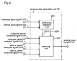
- FIG. 2 is a block diagram illustrating a detailed structure of the window pulse generation unit 101, which will be described hereinafter.
- a differential operation unit 201 receives the horizontal sync signal S102 and the vertical sync signal S103 which are extracted from the video signal, detects a rising or falling edge of the horizontal sync signal S102, and outputs a differentiated signal, i.e., a horizontal differential signal S210.
- the differential operation unit 201 further detects a rising or falling edge of the vertical sync signal S103, and outputs a differentiated signal, i.e., a vertical differential signal S211.
- the sampling unit 201 receives the horizontal period start point signal S104, the horizontal period end point signal S105, the vertical period start point signal S106, the vertical period end point signal S107, the horizontal differential signal S210 and the vertical differential signal S211, and decides a window pulse signal S110 indicating a period for sampling the luminance signal.
- the sampling unit 202 is reset in accordance with the horizontal differential signal S210, and counts a reference clock, thereby calculating a horizontal period. Then, the sampling unit 202 sets a significant period within the horizontal period, indicated by the horizontal period start point signal S104 and the horizontal period end point signal S105, as a horizontal window.
- sampling unit 202 is reset in accordance with the vertical differential signal S211, and counts values loaded in accordance with the horizontal differential signal S210, thereby calculating a vertical period. Then, the sampling unit 202 sets a significant period within the vertical period, indicated by the vertical period start point signal S106 and the vertical period end point signal S107, as a vertical window.
- a signal indicating a period that is common to the horizontal window signal and the vertical window signal is a window pulse signal S110. This common period is a period during which the luminance signal is sampled.
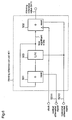
- Figure 3 is a block diagram illustrating a detailed structure of the bit shift unit 104, which will be described hereinafter.
- a significant bit detection unit 301 receives the number-of-pixel total sum signal S112, performs bit shift from the MSB of the number-of-pixel total sum signal S112 toward lower-order bits, to detect a first bit "1", i.e., a significant bit, and outputs a significant bit signal S310 indicating which bit counting from the MSB the significant bit is.
- a luminance value bit shift unit 302 receives the luminance value total sum signal S111 and the significant bit signal S301, and outputs a shifted total luminance sum signal S113 that is obtained by extracting a required number of bits from the luminance value total sum signal S111, on the basis of the significant bit signal S310.
- a number-of-pixel bit shift unit 303 receives the number-of-pixel total sum signal S112 and the significant bit signal S310, and outputs a shifted total number-of-pixel sum signal S114 that is obtained by extracting a required number of bits from the number-of-pixel total sum signal S112, on the basis of the significant bit signal S310.
- Figure 4 shows a specific example of the operation of the bit shift unit 104, which will be described hereinafter.
- the luminance value total sum signal S111 is 10-bit data which is represented as 1A6 in hexadecimal notation
- the number-of-pixel total sum signal S112 is 10-bit data which is represented as 9C in hexadecimal notation.
- the significant bit detection unit 301 receives the number-of-pixel total sum signal S112, and performs bit shift successively from the MSB of the number-of-pixel total sum signal S112 toward lower-order bits. In figure 4, since the MSB is "0", the bit shift is performed toward the next bit that is the second bit from the MSB. Because the second bit from the MSB is "1", the significant bit detection unit 301 outputs a significant bit signal S310 indicating that significant data starts from the second bit from the MSB (bit enclosed by a black rectangle).
- the luminance value bit shift unit 302 receives the luminance value total sum signal S111 and the significant bit signal S310. Since the inputted significant bit signal S310 indicates that the significant data starts from the second bit from the MSB, when for example 8 bits are required for detecting the average luminance level, the luminance value bit shift unit 302 extracts a significant data section 10 of 8 bits starting from the second bit from the MSB of the luminance value total sum signal S111. The extracted significant data unit 10 is 4E in hexadecimal notation, resulting in a shifted total luminance sum signal S113.
- the number-of-pixel bit shift unit 303 receives the number-of-pixel total sum signal S112 and the significant bit signal S310, and, when 8 bits are required for detecting the average luminance level, extracts a significant data section 20 of 8 bits starting from the second bit from the MSB of the number-of-pixel total sum signal S112.
- the extracted significant data section 20 is D3 in hexadecimal notation, resulting in a shifted total pixel sum signal S114.
- the luminance signal processing apparatus subjects the luminance value total sum signal S111 and the number-of-pixel total sum signal S112 to the bit shift, and detects the average luminance level on the basis of the shifted total luminance sum signal S113 and the shifted total pixel sum signal S114 comprising optimum significant bits. Therefore, average luminance levels according to plural video signal formats which have different numbers of significant pixels, such as 720p, 1080i, 525i, and 525p, can be detected by a small scale circuit with minimizing a rounded error, and with great accuracy.
- the luminance value total sum signal S111 is 10-bit data and represented as 1A6 in hexadecimal notation, while the luminance value total sum signal may be data of any bits and may be represented in any numbering system.
- the number-of-pixel total sum signal S112 is 10-bit data and represented as 9C in hexadecimal notation, while the number-of-pixel total sum signal may be data of any bits and may be represented in any numbering system.
- 8 bits are required in the luminance value bit shift unit 302 and the number-of-pixel bit shift unit 303, while the number of bits is not limited to 8 bits and any number of bits can be used in these units.
- the luminance signal S101 is inputted to the luminance value addition unit 102, while the luminance signal S102 may be passed through a low-pass filter and then inputted to the luminance value addition unit 102.
- the luminance signal S101 is passed through the low-pass filter, noises are eliminated, and accordingly a more accurate average luminance level can be detected.
- a luminance signal processing apparatus according to a second embodiment of the present invention will be hereinafter described.
- This second embodiment is different from the first embodiment only in the structure of the window pulse generation unit 101. Therefore, the window pulse generation unit 101 will be described with reference to figure 5.
- Figure 5 is a block diagram illustrating the window pulse generation unit 101 according to the second embodiment.
- the window pulse generation unit 101 receives the horizontal sync signal S102 and the vertical sync signal S103 which are extracted from the video signal, the horizontal period start point signal S104, the horizontal period end point signal S105, the vertical period start point signal S106 and the vertical period end point signal S107, and outputs a window pulse signal S410.
- a differential operation unit 201 receives the horizontal sync signal S102 and the vertical sync signal S103 which are extracted from the video signal, detects a rising or falling edge of the horizontal sync signal S102, and outputs a differentiated signal, i.e., a horizontal differential signal S210.
- the differential operation unit 201 further detects a rising or falling edge of the vertical sync signal S103, and outputs a differentiated signal, i.e., a vertical differential signal S211.
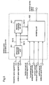
- a thinning reference set unit 401 receives the horizontal differential signal S210 and the vertical differential signal S211, and outputs a thinning reference value S411.
- the thinning reference set unit 401 will be described with reference to figure 6.
- the thinning reference set unit 401 is initially reset by means of a counter 501 in accordance with the vertical differential signal S211, then performs loading by a load/hold means 503 in accordance with the horizontal differential signal S210, and counts loaded values as inputs of the counter 501, thereby calculating the number of lines.
- a number of bits that are to be extracted from the number of lines, which are outputted from the load/hold means 503, i.e., n bits are taken out from less significant bits.
- the values that can be extracted vary with line numbers by the number of bits extracted, i.e., n bits.
- the counter 502 is reset in accordance with the horizontal differential signal S210, and counts a reference clock.
- the counter 502 since the counter 502 counts the reference clock with taking less significant "n" bits which are outputted from the load/hold means 503 as the initial value, the values at which the counter starts counting vary with lines.
- the output of this counter 502 is a thinning reference value S411.
- the counter 502 is a counter for the number of bits to be taken out, i.e., "n" bits.
- the counter 501 may be the counter for the number of bits to be taken out, i.e., "n" bits.
- figure 7(a) shows the thinning reference value S411 in a case where less significant 2 bits are taken out from the counter 501 and the value of the 1st line is 00 in binary representation.
- Figure 7(a) is a diagram showing the thinning reference value S411 so as to correspond to a display screen. One rectangular corresponds to one pixel on the display screen, and the vertical axis corresponds to lines. In figure 7(a), the values at which the counter starts counting vary with lines.
- the value of the thinning reference value S411 corresponding to the 2nd line is 01 in binary representation
- the value of the 3rd line is 10 in binary representation
- the value of the 4th line is 11 in binary representation
- the value of the 5th line is 00 in binary representation.
- the sampling unit 402 receives the horizontal period start point signal S104, the horizontal period end point signal S105, the vertical period start point signal S106, the vertical period end point signal S107, the horizontal differential signal S210, the vertical differential signal S211 and the thinning reference value S411, and generates a window pulse signal S410 that indicates a period during which the luminance signal is sampled.
- the sampling unit 402 is reset in accordance with the horizontal differential signal S210, and counts a reference clock, thereby calculating the horizontal period. Then, a significant period within the horizontal period, which is indicated by the horizontal period start point signal S104 and the horizontal period end point signal S105, is set as a horizontal window. In addition, the sampling unit 402 is reset in accordance with the vertical differential signal S211, and counts values that are loaded in accordance with the horizontal differential signal S210, thereby calculating the vertical period. Then, a significant period within the vertical period, indicated by the vertical period start point signal S106 and the vertical period end point signal S107, is set as a vertical window.
- the sampling unit 402 in order to take out values for sampling the luminance signal, the sampling unit 402 generates a thinning pulse on the basis of the thinning reference value S411.
- the thinning reference value S411 matches a predetermined value, a pulse is generated, and this generated pulse is used as the thinning pulse.
- the predetermined value is one of values corresponding to less significant bits which are extracted from the output of the counter 501, i.e., values which the bits to be extracted may take. For example, when less significant 2 bits are extracted from the output of the counter 501, the value corresponding to the bits to be extracted may take 0 to 3, and then a pulse is generated when the thinning reference value S411 matches with one of these values. Therefore, the thinning pulse can be generated for each bit to be extracted.
- a signal indicating a period which is common among the thinning pulse that has been generated as described above, the horizontal window, and the vertical window is set as the window pulse signal S410.
- This common period is a period during which the luminance signal is sampled.
- Figure 7(a) is a diagram showing the thinning reference value S411 so as to correspond to the display screen, as described above.
- a window pulse signal S410 indicating a period that is common among the thinning pulse, the horizontal window, and the vertical window is shown in figure 7(b).
- Figure 7 (c) is a diagram showing the window pulse signal S410 shown in figure 7(b) so as to correspond to the display screen.
- pixels corresponding to diagonally shaded areas are pixels within a period during which the luminance signal is sampled, indicated by the window pulse signal S410.
- luminance values of the luminance signal in the period indicated by the window pulse signal S410 that is obtained as described above are added, and the average luminance level is detected.
- the window pulse generation unit 101 generates a thinning pulse on the basis of the thinning reference value S411 that is outputted from the thinning reference set unit 401, as well as generates the window pulse signal S410 indicating a period that is common among the horizontal window which is obtained by the horizontal differential signal S210, the horizontal period start point signal S104 and the horizontal period end point signal S105, and the vertical window which is obtained by the vertical differential signal S211, the vertical period start point signal S106 and the vertical period end point signal S107, and the thinning pulse, then adds luminance values within the period indicated by the window pulse signal S410 by means of the luminance value addition unit 102, and adds the numbers of pixels within the period indicated by the window pulse signal S410 by means of the number-of-pixel addition unit 103. Therefore, when the average luminance level is to be detected, the total sums of the luminance values and the numbers of pixels can be reduced, thereby reducing the circuit scale.
- the thinning reference value comprises 2 bits, while the number of bits is not limited to 2 bits and this thinning reference value may comprise any number of bits which are to be taken out.
- the luminance signal processing apparatus is suitable for detecting an average luminance level of a video signal, adaptively to various video signal formats having different numbers of significant pixels, such as 720p, 1080i, 525i, and 525p.
Landscapes
- Engineering & Computer Science (AREA)
- Multimedia (AREA)
- Signal Processing (AREA)
- Physics & Mathematics (AREA)
- Computer Hardware Design (AREA)
- General Physics & Mathematics (AREA)
- Theoretical Computer Science (AREA)
- Picture Signal Circuits (AREA)
- Control Of Indicators Other Than Cathode Ray Tubes (AREA)
- Controls And Circuits For Display Device (AREA)
Abstract
Description
Claims (3)
- A luminance signal processing apparatus including:a window pulse generation means for generating a window pulse signal that indicates a period during which a luminance signal of an input video signal is sampled;a luminance value addition means for obtaining a total sum of luminance values of the luminance signal in the period indicated by the window pulse signal;a number-of-pixel addition means for obtaining the number of pixels in the period indicated by the window pulse signal;a bit shift means for detecting a significant bit from an output signal of the number-of-pixel addition means, and bit-shifting the output signal of the number-of-pixel addition means and an output signal of the luminance value addition means, respectively, on the basis of the significant bit; anda division means for dividing the bit-shifted output signal of the luminance value addition means, by the bit-shifted output signal of the number-of-pixel addition means, thereby obtaining an average luminance level in the period during which the luminance signal is sampled.
- The luminance signal processing apparatus of Claim 1 wherein
the bit shift means includes:a significant bit detection means for shifting the output signal of the number-of-pixel addition means successively from its most significant bit, and detecting a significant bit;a number-of-pixel bit shift means for extracting a predetermined number of bits from the output signal of the number-of-pixel addition means on the basis of an output signal of the significant bit detection means; anda luminance value bit shift means for extracting the predetermined number of bits from the output signal of the luminance value addition means on the basis of the output signal of the significant bit detection means. - The luminance signal processing apparatus of Claim 1 wherein
the window pulse generation means includes:a differentiation means for detecting rising or falling edges of a horizontal synchronizing signal and a vertical synchronizing signal of the input video signal, differentiating the same, and outputting a horizontal differential signal and a vertical differential signal;a thinning reference value set means that includes: a first counter which is reset in accordance with the vertical differential signal, and counts values which are loaded in accordance with the horizontal differential signal, thereby counting the number of lines; and a second counter for n bits, which is reset in accordance with the horizontal differential signal and counts a reference clock with taking a value corresponding to less significant n bits which are extracted from a value that is obtained by loading an output of the first counter, as an initial value, and outputs a value which is counted being shifted by one for each line, as a thinning reference value that is used when values of the luminance signal to be sampled are taken out; anda sampling means for receiving a vertical period start point signal, a vertical period end point signal, a horizontal period start point signal and a horizontal period end point signal, being reset in accordance with the vertical differential signal, obtaining a period indicated by the vertical period start point signal and the vertical period end point signal, within a vertical period that is obtained by counting values loaded in accordance with the horizontal differential signal, as a first significant period, further being reset in accordance with the horizontal differential signal, obtaining a period indicated by the horizontal period start point signal and the horizontal period end point signal, within a horizontal period that is obtained by counting a reference clock, as a second significant period, then generating a thinning pulse when the thinning reference value matches a predetermined value, and generating a window pulse signal indicating a period that is common among the first significant period, the second significant period and the thinning pulse.
Applications Claiming Priority (3)
| Application Number | Priority Date | Filing Date | Title |
|---|---|---|---|
| JP33388199 | 1999-11-25 | ||
| JP33388199 | 1999-11-25 | ||
| PCT/JP2000/008276 WO2001039489A1 (en) | 1999-11-25 | 2000-11-24 | Apparatus for processing luminance signal |
Publications (2)
| Publication Number | Publication Date |
|---|---|
| EP1235425A1 true EP1235425A1 (en) | 2002-08-28 |
| EP1235425A4 EP1235425A4 (en) | 2006-01-11 |
Family
ID=18271005
Family Applications (1)
| Application Number | Title | Priority Date | Filing Date |
|---|---|---|---|
| EP00977897A Withdrawn EP1235425A4 (en) | 1999-11-25 | 2000-11-24 | APPARATUS FOR PROCESSING A LUMINANCE SIGNAL |
Country Status (7)
| Country | Link |
|---|---|
| US (1) | US6967692B1 (en) |
| EP (1) | EP1235425A4 (en) |
| JP (1) | JP3712976B2 (en) |
| KR (1) | KR100434632B1 (en) |
| CN (1) | CN1165157C (en) |
| TW (1) | TW502528B (en) |
| WO (1) | WO2001039489A1 (en) |
Families Citing this family (3)
| Publication number | Priority date | Publication date | Assignee | Title |
|---|---|---|---|---|
| JP2007529778A (en) * | 2004-03-19 | 2007-10-25 | コーニンクレッカ フィリップス エレクトロニクス エヌ ヴィ | Active matrix display with improved non-uniformity between pixels at low brightness |
| JP4031462B2 (en) * | 2004-04-23 | 2008-01-09 | 松下電器産業株式会社 | Luminance signal processing device, signal processing device, and luminance signal processing method |
| IL165852A (en) * | 2004-12-19 | 2010-12-30 | Rafael Advanced Defense Sys | System and method for image display enhancement |
Family Cites Families (8)
| Publication number | Priority date | Publication date | Assignee | Title |
|---|---|---|---|---|
| FR2575885B1 (en) | 1985-01-04 | 1987-02-20 | Thomson Csf | CONTRAST ENHANCER FOR VIDEO IMAGES |
| JPH089196A (en) | 1994-06-20 | 1996-01-12 | Fujitsu General Ltd | Average brightness calculation circuit |
| KR0142262B1 (en) * | 1994-08-31 | 1998-06-15 | 김광호 | Automatic high brightness compression circuit |
| TW344931B (en) * | 1994-12-08 | 1998-11-11 | Matsushita Electric Industrial Co Ltd | Average luminance level detection apparatus and aspect ratio auto-discrimination apparatus for a television signal using the same |
| JPH08202319A (en) | 1995-01-20 | 1996-08-09 | Fujitsu General Ltd | Video signal level detector |
| JP2964923B2 (en) | 1995-08-16 | 1999-10-18 | 日本電気株式会社 | Image processing apparatus and image processing method |
| US5805238A (en) * | 1996-05-14 | 1998-09-08 | Raytheon Company | Adaptive notch filter for removing residual subcarrier from component video |
| US6313883B1 (en) * | 1999-09-22 | 2001-11-06 | Vista Medical Technologies, Inc. | Method and apparatus for finite local enhancement of a video display reproduction of images |
-
2000
- 2000-11-22 TW TW089124746A patent/TW502528B/en not_active IP Right Cessation
- 2000-11-24 KR KR10-2002-7006578A patent/KR100434632B1/en not_active Expired - Fee Related
- 2000-11-24 CN CNB008161879A patent/CN1165157C/en not_active Expired - Fee Related
- 2000-11-24 EP EP00977897A patent/EP1235425A4/en not_active Withdrawn
- 2000-11-24 US US10/130,624 patent/US6967692B1/en not_active Expired - Fee Related
- 2000-11-24 JP JP2001540513A patent/JP3712976B2/en not_active Expired - Fee Related
- 2000-11-24 WO PCT/JP2000/008276 patent/WO2001039489A1/en not_active Ceased
Also Published As
| Publication number | Publication date |
|---|---|
| CN1165157C (en) | 2004-09-01 |
| KR100434632B1 (en) | 2004-06-04 |
| US6967692B1 (en) | 2005-11-22 |
| TW502528B (en) | 2002-09-11 |
| EP1235425A4 (en) | 2006-01-11 |
| KR20020059775A (en) | 2002-07-13 |
| CN1399842A (en) | 2003-02-26 |
| JP3712976B2 (en) | 2005-11-02 |
| WO2001039489A1 (en) | 2001-05-31 |
Similar Documents
| Publication | Publication Date | Title |
|---|---|---|
| US6366706B1 (en) | Method and apparatus for automatic aspect format detection in digital video pictures | |
| US6313881B1 (en) | Signal processing for a picture signal | |
| US5933196A (en) | Pixel conversion apparatus | |
| US6229574B1 (en) | Screen ratio converter for digital TV | |
| EP0675645A2 (en) | Apparatus for discriminating video kinds and automatic aspect ratio discrimination apparatus and television receiver using it | |
| EP0720367A2 (en) | Method and apparatus for identifying video fields produced by film sources | |
| US20070222895A1 (en) | Subtitle detection apparatus, subtitle detection method and pull-down signal detection apparatus | |
| KR100196553B1 (en) | Letterbox signal processing system with logo and closed caption | |
| EP0455957B1 (en) | Odd/even field detector for video signals | |
| EP0969658A1 (en) | Noise reduction signal processing circuit and display apparatus | |
| JPH02199970A (en) | System for determining sequence position of video fields obtained from film | |
| US20050243204A1 (en) | Conversion of interlaced video streams into progressive video streams | |
| US7082161B2 (en) | Television/cinema scheme identification apparatus and identification method | |
| US6965414B2 (en) | Apparatus for detecting telecine conversion method of video signal | |
| US4677482A (en) | Dual mode progressive scan system with automatic mode switching by image analysis | |
| EP1641270A1 (en) | Block distortion detection device, block distortion detection method, and video signal processing device | |
| US6667766B2 (en) | Method of removing noise from image signal | |
| US6967692B1 (en) | Apparatus for processing luminance signal | |
| US5686970A (en) | Average luminance level detection apparatus and aspect ratio auto-discrimination apparatus for a television signal using the same | |
| EP1018262B1 (en) | Video signal character converting device and method of the same | |
| JPWO2001039489A1 (en) | Luminance signal processing device | |
| JP3232950B2 (en) | Video type identification device, automatic aspect ratio identification device and television receiver using the same | |
| EP0913994B1 (en) | Method and apparatus for automatic format detection in digital video pictures | |
| US7636129B2 (en) | Method and device for detecting sawtooth artifact and/or field motion | |
| EP0802686A2 (en) | Signal processing system |
Legal Events
| Date | Code | Title | Description |
|---|---|---|---|
| PUAI | Public reference made under article 153(3) epc to a published international application that has entered the european phase |
Free format text: ORIGINAL CODE: 0009012 |
|
| 17P | Request for examination filed |
Effective date: 20020618 |
|
| AK | Designated contracting states |
Kind code of ref document: A1 Designated state(s): AT BE CH CY DE DK ES FI FR GB GR IE IT LI LU MC NL PT SE TR |
|
| AX | Request for extension of the european patent |
Free format text: AL;LT;LV;MK;RO;SI |
|
| RIN1 | Information on inventor provided before grant (corrected) |
Inventor name: ITO, KEIICHI Inventor name: KAGEYAMA, ATSUHISA Inventor name: KAKUYA, YUKI Inventor name: OKADA, NOBUTAKA |
|
| A4 | Supplementary search report drawn up and despatched |
Effective date: 20051128 |
|
| 17Q | First examination report despatched |
Effective date: 20080226 |
|
| RAP1 | Party data changed (applicant data changed or rights of an application transferred) |
Owner name: PANASONIC CORPORATION |
|
| APBK | Appeal reference recorded |
Free format text: ORIGINAL CODE: EPIDOSNREFNE |
|
| APBN | Date of receipt of notice of appeal recorded |
Free format text: ORIGINAL CODE: EPIDOSNNOA2E |
|
| APBR | Date of receipt of statement of grounds of appeal recorded |
Free format text: ORIGINAL CODE: EPIDOSNNOA3E |
|
| APAF | Appeal reference modified |
Free format text: ORIGINAL CODE: EPIDOSCREFNE |
|
| APBT | Appeal procedure closed |
Free format text: ORIGINAL CODE: EPIDOSNNOA9E |
|
| STAA | Information on the status of an ep patent application or granted ep patent |
Free format text: STATUS: THE APPLICATION IS DEEMED TO BE WITHDRAWN |
|
| 18D | Application deemed to be withdrawn |
Effective date: 20120601 |