EP1232998A1 - Low-permittivity porous siliceous film, semiconductor devices having such films, and coating composition for forming the film - Google Patents
Low-permittivity porous siliceous film, semiconductor devices having such films, and coating composition for forming the film Download PDFInfo
- Publication number
- EP1232998A1 EP1232998A1 EP00937325A EP00937325A EP1232998A1 EP 1232998 A1 EP1232998 A1 EP 1232998A1 EP 00937325 A EP00937325 A EP 00937325A EP 00937325 A EP00937325 A EP 00937325A EP 1232998 A1 EP1232998 A1 EP 1232998A1
- Authority
- EP
- European Patent Office
- Prior art keywords
- coating
- polysilazane
- silica coating
- porous silica
- aluminum
- Prior art date
- Legal status (The legal status is an assumption and is not a legal conclusion. Google has not performed a legal analysis and makes no representation as to the accuracy of the status listed.)
- Granted
Links
Classifications
-
- C—CHEMISTRY; METALLURGY
- C01—INORGANIC CHEMISTRY
- C01B—NON-METALLIC ELEMENTS; COMPOUNDS THEREOF; METALLOIDS OR COMPOUNDS THEREOF NOT COVERED BY SUBCLASS C01C
- C01B33/00—Silicon; Compounds thereof
- C01B33/113—Silicon oxides; Hydrates thereof
- C01B33/12—Silica; Hydrates thereof, e.g. lepidoic silicic acid
-
- C—CHEMISTRY; METALLURGY
- C09—DYES; PAINTS; POLISHES; NATURAL RESINS; ADHESIVES; COMPOSITIONS NOT OTHERWISE PROVIDED FOR; APPLICATIONS OF MATERIALS NOT OTHERWISE PROVIDED FOR
- C09D—COATING COMPOSITIONS, e.g. PAINTS, VARNISHES OR LACQUERS; FILLING PASTES; CHEMICAL PAINT OR INK REMOVERS; INKS; CORRECTING FLUIDS; WOODSTAINS; PASTES OR SOLIDS FOR COLOURING OR PRINTING; USE OF MATERIALS THEREFOR
- C09D183/00—Coating compositions based on macromolecular compounds obtained by reactions forming in the main chain of the macromolecule a linkage containing silicon, with or without sulfur, nitrogen, oxygen, or carbon only; Coating compositions based on derivatives of such polymers
- C09D183/16—Coating compositions based on macromolecular compounds obtained by reactions forming in the main chain of the macromolecule a linkage containing silicon, with or without sulfur, nitrogen, oxygen, or carbon only; Coating compositions based on derivatives of such polymers in which all the silicon atoms are connected by linkages other than oxygen atoms
-
- H—ELECTRICITY
- H10—SEMICONDUCTOR DEVICES; ELECTRIC SOLID-STATE DEVICES NOT OTHERWISE PROVIDED FOR
- H10P—GENERIC PROCESSES OR APPARATUS FOR THE MANUFACTURE OR TREATMENT OF DEVICES COVERED BY CLASS H10
- H10P14/00—Formation of materials, e.g. in the shape of layers or pillars
- H10P14/60—Formation of materials, e.g. in the shape of layers or pillars of insulating materials
- H10P14/65—Formation of materials, e.g. in the shape of layers or pillars of insulating materials characterised by treatments performed before or after the formation of the materials
- H10P14/6516—Formation of materials, e.g. in the shape of layers or pillars of insulating materials characterised by treatments performed before or after the formation of the materials of treatments performed after formation of the materials
- H10P14/6529—Formation of materials, e.g. in the shape of layers or pillars of insulating materials characterised by treatments performed before or after the formation of the materials of treatments performed after formation of the materials by exposure to a gas or vapour
-
- H—ELECTRICITY
- H10—SEMICONDUCTOR DEVICES; ELECTRIC SOLID-STATE DEVICES NOT OTHERWISE PROVIDED FOR
- H10P—GENERIC PROCESSES OR APPARATUS FOR THE MANUFACTURE OR TREATMENT OF DEVICES COVERED BY CLASS H10
- H10P14/00—Formation of materials, e.g. in the shape of layers or pillars
- H10P14/60—Formation of materials, e.g. in the shape of layers or pillars of insulating materials
- H10P14/66—Formation of materials, e.g. in the shape of layers or pillars of insulating materials characterised by the type of materials
- H10P14/668—Formation of materials, e.g. in the shape of layers or pillars of insulating materials characterised by the type of materials the materials being characterised by the deposition precursor materials
- H10P14/6681—Formation of materials, e.g. in the shape of layers or pillars of insulating materials characterised by the type of materials the materials being characterised by the deposition precursor materials the precursor containing a compound comprising Si
- H10P14/6687—Formation of materials, e.g. in the shape of layers or pillars of insulating materials characterised by the type of materials the materials being characterised by the deposition precursor materials the precursor containing a compound comprising Si the compound comprising silicon and nitrogen
- H10P14/6689—Formation of materials, e.g. in the shape of layers or pillars of insulating materials characterised by the type of materials the materials being characterised by the deposition precursor materials the precursor containing a compound comprising Si the compound comprising silicon and nitrogen the compound being a silazane
-
- H—ELECTRICITY
- H10—SEMICONDUCTOR DEVICES; ELECTRIC SOLID-STATE DEVICES NOT OTHERWISE PROVIDED FOR
- H10P—GENERIC PROCESSES OR APPARATUS FOR THE MANUFACTURE OR TREATMENT OF DEVICES COVERED BY CLASS H10
- H10P14/00—Formation of materials, e.g. in the shape of layers or pillars
- H10P14/60—Formation of materials, e.g. in the shape of layers or pillars of insulating materials
- H10P14/69—Inorganic materials
- H10P14/692—Inorganic materials composed of oxides, glassy oxides or oxide-based glasses
- H10P14/6921—Inorganic materials composed of oxides, glassy oxides or oxide-based glasses containing silicon
- H10P14/69215—Inorganic materials composed of oxides, glassy oxides or oxide-based glasses containing silicon the material being a silicon oxide, e.g. SiO2
-
- H—ELECTRICITY
- H10—SEMICONDUCTOR DEVICES; ELECTRIC SOLID-STATE DEVICES NOT OTHERWISE PROVIDED FOR
- H10P—GENERIC PROCESSES OR APPARATUS FOR THE MANUFACTURE OR TREATMENT OF DEVICES COVERED BY CLASS H10
- H10P14/00—Formation of materials, e.g. in the shape of layers or pillars
- H10P14/60—Formation of materials, e.g. in the shape of layers or pillars of insulating materials
- H10P14/63—Formation of materials, e.g. in the shape of layers or pillars of insulating materials characterised by the formation processes
- H10P14/6326—Deposition processes
- H10P14/6342—Liquid deposition, e.g. spin-coating, sol-gel techniques or spray coating
-
- H—ELECTRICITY
- H10—SEMICONDUCTOR DEVICES; ELECTRIC SOLID-STATE DEVICES NOT OTHERWISE PROVIDED FOR
- H10P—GENERIC PROCESSES OR APPARATUS FOR THE MANUFACTURE OR TREATMENT OF DEVICES COVERED BY CLASS H10
- H10P14/00—Formation of materials, e.g. in the shape of layers or pillars
- H10P14/60—Formation of materials, e.g. in the shape of layers or pillars of insulating materials
- H10P14/66—Formation of materials, e.g. in the shape of layers or pillars of insulating materials characterised by the type of materials
- H10P14/665—Porous materials
-
- H—ELECTRICITY
- H10—SEMICONDUCTOR DEVICES; ELECTRIC SOLID-STATE DEVICES NOT OTHERWISE PROVIDED FOR
- H10P—GENERIC PROCESSES OR APPARATUS FOR THE MANUFACTURE OR TREATMENT OF DEVICES COVERED BY CLASS H10
- H10P14/00—Formation of materials, e.g. in the shape of layers or pillars
- H10P14/60—Formation of materials, e.g. in the shape of layers or pillars of insulating materials
- H10P14/69—Inorganic materials
- H10P14/692—Inorganic materials composed of oxides, glassy oxides or oxide-based glasses
- H10P14/6921—Inorganic materials composed of oxides, glassy oxides or oxide-based glasses containing silicon
- H10P14/6922—Inorganic materials composed of oxides, glassy oxides or oxide-based glasses containing silicon the material containing Si, O and at least one of H, N, C, F or other non-metal elements, e.g. SiOC, SiOC:H or SiONC
Definitions
- the present invention relates to a porous silica coating with a low dielectric constant, a semiconductor device comprising the porous silica coating, and a coating composition which becomes the porous silica coating.
- silica coatings are converted into silica coatings by firing in atmospheric air. These silica coatings are used as interlayer dielectrics for semiconductors because of excellent electrical insulating properties. Among these silica coatings, a completely inorganic silica coating has already been employed as an excellent interlayer dielectric for a semiconductor because it has high heat resistance and can be used in a non-etch back process. In this case, the physical properties of the silica coating are similar to those of silicon dioxide (SiO 2 ) and its dielectric constant is within a range from 3.0 to 4.7.
- the dielectric constant of a conventional silica coating is too high for such a requirement. It is known to make the silica coating porous so as to reduce the dielectric constant, however, the silica coating generally has moisture absorption properties and the dielectric constant increases with the elapse of time, under an ambient atmosphere. It has been proposed that a porous coating is subjected to a water repellent treatment thereby to add an organic group such as a trimethylsilyl group to the surface in order to prevent an increase in dielectric constant with the elapse of time due to moisture absorption. However, such an additional water repellent treatment causes the problem that the manufacturing cost increases and introduction of the organic group impairs an inorganic material's ability to make it possible to be used in a non-etch back process.
- an object of the present invention to provide a silica coating which makes it possible to drastically reduce the dielectric constant (especially to less than 2.5) and to substantially maintain the reduced dielectric constant under an ambient atmosphere without being subjected to a water repellent treatment.
- Another object of the present invention is to provide a semiconductor device comprising the silica coating with such a low dielectric constant as an interlayer dielectric, and a coating composition which becomes the silica coating.
- a porous silica coating having a dielectric constant of less than 2.5 which is obtained by firing a coating of a composition comprising an aluminum-containing polysilazane and a polyacrylate or polymethacrylate ester.
- a semiconductor device comprising the porous silica coating as an interlayer dielectric.
- a coating composition comprising an aluminum-containing polysilazane and a polyacrylate or polymethacrylate ester in an organic solvent.
- the porous silica coating of the present invention is obtained by firing a coating of a composition comprising an aluminum-containing polysilazane and a polyacrylate or polymethacrylate ester.
- the aluminum-containing polysilazane is obtained by mixing a polysilazane with an aluminum compound.
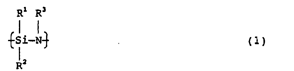
- the polysilazane as a material for forming the silica coating has in its molecular chain a silazane structure represented by the following general formula (1):
- R 1 , R 2 and R 3 each independently represents a hydrogen atom, a hydrocarbon group, a hydrocarbon group-containing silyl group, a hydrocarbon group-containing amino group, or a hydrocarbonoxy group. At least one of R 1 and R 2 represents a hydrogen atom.
- the hydrocarbon group may be combined with a substituent, and examples of the substituent include halogen such as chlorine, bromine and fluorine, an alkoxy group, an alkoxycarbonyl group, and an amino group.
- the hydrocarbon group includes an aliphatic hydrocarbon group and an aromatic hydrocarbon group, and the aliphatic hydrocarbon group includes a chain hydrocarbon group and a cyclic hydrocarbon group.
- the hydrocarbon group include an alkyl group, an alkenyl group, a cycloalkyl group, a cycloalkenyl group, an aryl group, and an arylalkyl group.
- the number of carbon atoms in these hydrocarbon atoms is not limited, but is usually 20 or less, and preferably 10 or less. In the present invention, preferred is an alkyl group having 1 to 8 carbon atoms, and particularly 1 to 4 carbon atoms.
- a preferable hydrocarbon group is an alkyl group having 1 to 20 carbon atoms, and particularly 1 to 6 carbon atoms.
- the number of hydrocarbon atoms to be combined with Si is within a range from 1 to 3.
- the number of carbon atoms in the hydrocarbon group is within a range from 1 to 3.
- the polysilazane having a silazane structure represented by the general formula (1) in a molecular chain may be a polysilazane having a chain, cyclic or crosslinked structure, or a mixture thereof.
- the number-average molecular weight is within a range from 100 to 100,000, and preferably from 300 to 10,000.
- Such a polysilazane includes conventional perhydropolysilazane, organopolysilazane, and a modified compound thereof.
- modified polysilazane examples include a platinum- or palladium-containing polysilazane, an alcohol residue-containing polysilazane, an HMDS (hexamethyldisilazane) residue-containing polysilazane, an amine-containing polysilazane, and an organic acid-containing polysilazane.
- the aluminum to be incorporated into the polysilazane may be an aluminum compound in the form capable of being dissolved in an organic solvent.
- a soluble aluminum compound includes an alkoxide, a chelete compound, an organoaluminum, and a halide.
- alkoxide of aluminum examples include those represented by the following general formula (2):
- R 4 , R 5 and R 6 represent a hydrocarbon group.
- the hydrocarbon group includes an aliphatic hydrocarbon group and an aromatic hydrocarbon group.
- the aliphatic hydrocarbon group includes a chain hydrocarbon group and a cyclic hydrocarbon group.
- Examples of the aliphatic hydrocarbon group include an alkyl group, an alkenyl group, a cycloalkyl group, and a cycloalkenyl group.
- the number of carbon atoms is not specifically limited, but is usually 20 or less, and preferably 8 or less.
- the aliphatic hydrocarbon group examples include methyl, ethyl, propyl, butyl, pentyl, octyl, dodecyl, octadecyl, dodecenyl, cyclohexyl, and cyclohexenyl.
- the aromatic hydrocarbon group includes an aryl group and an arylalkyl group. Specific examples of the aromatic hydrocarbon group include phenyl, tolyl, xylyl, naphthyl, benzyl, phenethyl, and naphthylmethyl.
- Examples of the chelete compound of aluminum include aluminum acetylacetonate and aluminum ethylacetonate.
- organoaluminum examples include those represented by the following general formula (3):
- R 4 , R 5 and R 6 represent a hydrocarbon group.
- the hydrocarbon group includes those described in connection with the general formula (2).
- halide of aluminum examples include those represented by the following general formula (4): AlX 3 (4) wherein X represents a halogen.
- the halogen includes chlorine, bromine, iodine, and fluorine.
- the organic solvent-soluble aluminum compounds can be used alone or in combination.
- the amount of the aluminum compound to be added to the polysilazane varies depending on the kind, but is within a range from 0.001 to 10% by weight as aluminum, preferably from 0.01 to 10% by weight, and more preferably from 0.1 to 1% by weight, on the basis of the polysilazane.
- the amount of the aluminum compound is larger than the range described above, the density and homogeneity of the resulting silica coating are lowered. Therefore, it is not preferred.
- the amount is smaller than the range, the effect of the added aluminum compound becomes insufficient.
- a polysilazane and an aluminum compound are mixed with stirring in an organic solvent.
- they are mixed with stirring under the conditions. of a temperature within a range from 0 to 200°C, preferably from 0 to 100°C, and a pressure within a range from normal pressure to 10 kg/cm 2 G, preferably normal pressure.
- the concentration of the polysilazane in the organic solvent is within a range from 0.1 to 80% by weight, and preferably from 5 to 50% by weight.
- an inert organic solvent free from active hydrogen is used.
- the organic solvent include an aromatic hydrocarbon solvent such as benzene, toluene, xylene, ethylbenzene, diethylbenzene, trimethylbenzene, or triethylbenzene; an alicyclic hydrocarbon solvent such as cyclohexane, cyclohexene, decahydronaphthalene, ethylcyclohexane, methylcyclohexane, p-menthine, or dipentene (limonene); an ether solvent such as dipropyl ether or dibutyl ether; and a ketone solvent such as methyl isobutyl ketone.
- An aluminum-containing polysilazane in which an aluminum compound is mixed or added, is formed by mixing the polysilazane and the aluminum compound with stirring in the organic solvent.
- the resulting aluminum-containing polysilazane does not have an aluminopolysilazane structure wherein aluminum and silicon are firmly combined.
- the coating composition of the present invention is obtained by adding a polyacrylate or polymethacrylate ester to an organic solvent solution containing the aluminum-containing polysilazane thus obtained.
- the polyacrylate or polymethacrylate ester which is useful in the present invention, is a homopolymer or copolymer of a polyacrylate or polymethacrylate ester, and specific examples thereof include polymethyl acrylate, polyethyl acrylate, polybutyl acrylate, polymethyl methacrylate, polyethyl methacrylate, polybutyl methacrylate, polyisobutyl methacrylate, and block copolymers and other copolymers thereof.
- the polyacrylate or polymethacrylate ester in the present invention those having a number-average molecular weight within a range from 1,000 to 800,000 are used.
- the number-average molecular weight is smaller than 1,000, a porous coating is not formed because the polyacrylate or polymethacrylate ester is sublimated at low temperature.
- the number-average molecular weight exceeds 800,000, the pore size increases to cause voids, thus reducing the coating strength. Therefore, both cases are not preferred.
- the number-average molecular weight of the polyacrylate or polymethacrylate ester in the present invention is preferably within a range from 10,000 to 600,00, and particularly preferred results are obtained when the number-average molecular weight is within a range from 50,000 to 300,000.
- the amount of the polyacrylate or polymethacrylate ester in the present invention is controlled within a range from 5 to 150% by weight based on the polysilazane used.
- the amount of the polyacrylate or polymethacrylate ester is smaller than 5% by weight, the coating is insufficiently made porous.
- the amount is larger than 150% by weight, defects such as voids and cracks occur, thereby to reduce the coating strength. Therefore, it is not preferred.
- the amount of the polyacrylate or polymethacrylate ester in the present invention is preferably within a range from 10 to 120% by weight, and particularly preferred results are obtained when the amount is within a range from 20 to 100% by weight.
- the polyacrylate or polymethacrylate ester is generally added to an aluminum-containing polysilazane solution in the form of a solution prepared by dissolving the polyester in an organic solvent.
- the same organic solvent as that used in preparation of the aluminum-containing polysilazane solution may be used as the organic solvent.
- an inert organic solvent free from active hydrogen described above is used as the organic solvent in which the polyacrylate or polymethacrylate ester is dissolved.
- the concentration of the polyacrylate or polymethacrylate ester can be controlled within a range from 5 to 80% by weight, and preferably from 10 to 40% by weight.
- a homogeneous solution can be obtained by physically stirring after the addition of the polyacrylate or polymethacrylate ester.
- the polyacrylate or polymethacrylate ester itself can also be added and dissolved in the aluminum-containing polysilazane solution.
- the coating composition of the present invention can be prepared by combining the polysilazane with the polyacrylate or polymethacrylate ester and mixing the aluminum compound therewith, or combining the polyacrylate or polymethacrylate ester with the aluminum compound and mixing the polysilazane therewith.
- the resulting organic solvent solution containing the aluminum-containing polysilazane and the polyacrylate or polymethacrylate ester can be coated on the surface of a substrate by using it as a coating composition with or without controlling the concentration of the polysilazane.
- Examples of the method of coating the coating composition containing the aluminum-containing polysilazane and the polyacrylate or polymethacrylate ester to the surface of the substrate include conventionally known methods, for example, spin coating method, dipping method, spraying method, and transferring method.
- the aluminum-containing polysilazane coating formed on the surface of the substrate is fired in various atmospheres.
- the atmosphere includes, for example, an atmosphere which scarcely contains water vapor, such as dry air, dry nitrogen, or dry helium, or an atmosphere containing water vapor, such as atmospheric air, moistened atmospheric air, or moistened nitrogen.
- the firing temperature is within a range from 50 to 600°C, and preferably from 300 to 500°C, and the firing time is within a range from one minute to one hour.
- a silica coating having a low dielectric constant and a good coating quality is advantageously prepared by forming a polysilazane coating on the surface of a substrate, preliminary heating the coating in a water vapor-containing atmosphere and firing the coating with heating in a dry atmosphere.
- the water vapor content in the water vapor-containing atmosphere, is 0.1 volume % or more, and preferably 1 volume % or more.
- the upper limit value is the dew point. Examples of such an atmosphere include atmospheric air, moistened atmospheric air, and moistened nitrogen gas.
- the water vapor content is 0.5 volume % or less, and preferably 0.05 volume % or less.
- dry atmosphere examples include dry air, nitrogen gas, argon gas, and helium gas.
- the preliminary heating temperature is within a range from 50 to 400°C, and preferably from 100 to 350°C.
- the firing temperature is within a range from 100 to 500°C, and preferably from 300 to 500°C.
- Si-H, Si-R (R: hydrocarbon group) and Si-N bonds in the polysilazane are oxidized and converted into Si-O bonds to form a silica coating.
- a Si-OH bond is not substantially formed.
- Si-H, Si-R and Si-N bonds are oxidized nearly simultaneously, although it varies depending on the conditions of firing. This fact is confirmed from the fact that absorptions based on Si-H, Si-R and Si-N disappear nearly simultaneously when the IR spectrum of the resulting silica coating is measured.
- the present invention allows the Si-O bond formed by selectively oxidizing the Si-N bond, and the unoxidized Si-H and Si-R bonds, to exist in the formed silica coating, thereby making it possible to obtain a silica coating with a low density.
- the dielectric constant of the silica coating is reduced with the reduction of the coating density, while adsorption of water as a high dielectric substance occurs when the coating density is reduced. Therefore, there arises a problem that the dielectric constant increases when the silica coating is left to stand in an atmospheric air.
- the silica coating containing Si-H and Si-R bonds of the present invention adsorption of water can be prevented regardless of low density because these bonds have water repellency.
- the silica coating of the present invention has a large merit that the dielectric constant of the coating scarcely increases even if the silica coating is left to stand in an atmospheric air containing water vapor.
- the silica coating of the present invention also has a merit that it is less likely to cause cracking because the internal stress of the coating is small due to low density.
- micropores having a diameter of 0.5 to 30 nm are formed in the silica coating by sublimation of the polyacrylate of polymethacrylate ester in the coating.
- the existence of the micropores further reduces the density of the silica coating, and thus the dielectric constant of the silica coating is further reduced. This is because the compatibility between the aluminum-containing polysilazane and the polyacrylate of polymethacrylate ester is very good.
- the use of the polyacrylate of polymethacrylate ester prevents the Si-OH bond from forming in the polysilazane during the firing of the coating.
- the silica coating maintains the water repellency and the dielectric constant reduced due to the micropores scarcely increases even when left to stand in an atmospheric air containing water vapor.
- a porous silica coating capable of stably maintaining a very low dielectric constant of less than 2.5, preferably 2.0 or less, occasionally about 1.6, in cooperation with the reduction in density and impartation of water repellency due to the bond component (SiH, SiR) of the silica coating as well as reduction in density of the whole coating due to micropores. Therefore, since a water repellent treatment required to prevent moisture absorption in a conventional porous silica coating is not required, it becomes advantageous in view of the manufacturing cost and an inorganic material's merit is not impaired by introduction of an organic group.
- the density is within a range from 0.5 to 1.4 g/cm 3 , and preferably from 0.7 to 1.1 g/cm 3
- the cracking limitation in coating thickness is 1.0 ⁇ m or more, and preferably 10 ⁇ m or more and, furthermore, the internal stress is 2.0 ⁇ 10 4 N/cm 2 or less, and preferably 1.0 ⁇ 10 4 N/cm 2 or less.
- the content of Si, which exists in the form of a Si-H or Si-R bond (R: hydrocarbon group), in the silica coating is within a range from 10 to 100 atomic %, and preferably from 25 to 75 atomic %, based on the number of Si atoms contained in the silica porous coating.
- the content of Si, which exists in the form of a Si-N bond, is 5 atomic % or less.
- the thickness of the silica coating obtained after firing varies depending on the purposes of the substrate surface, but is usually within a range from 0.01 to 5 ⁇ m, and preferably from 0.1 to 2 ⁇ m. When using as an interlayer dielectric, the thickness is within a range from 0.1 to 2 ⁇ m.
- an inorganic coating with a low dielectric constant which is composed only of elements of Si, O and H and has a Si-H bond but substantially has neither an N-H bond nor a Si-OH bond. Since this coating is superior in resistance to plasma, a so-called etch-back process of removing a coating layer on the metal wiring in a process of manufacturing a semiconductor can be omitted by applying this coating in the manufacture of the semiconductor. Therefore, the process of manufacturing the semiconductor can be markedly simplified.
- the porous silica coating of the present invention has a low density and has a merit that a cracking limitation in coating thickness, namely, a maximum coating thickness where a coating can be formed without causing cracking of the coating is 5 ⁇ m or more.
- a cracking limitation in coating thickness is within a range from about 0.5 to 1.5 ⁇ m. Therefore, the silica coating of the present invention exhibits a large technical effect as compared with a conventional silica coating.
- the method of forming the silica coating of the present invention can be carried out very easily because the aluminum-containing polysilazane, as a precursor thereof, can be converted into a silica coating at a firing temperature lower than 450°C even in a dry atmospheric air by a catalytic action of aluminum.
- the present invention is advantageously applied as a method of forming an insulating coating to an aluminum wiring whose heat-resistant upper limit temperature is 450°C. According to the present invention, since the content of the Si-N bond can be substantially reduced to 0% by a catalytic action of aluminum, the coating has very high stability and is not deteriorated even when left to stand in atmospheric air.
- the silica coating of the present invention can be advantageously used as an interlayer dielectric in a semiconductor device.
- the silica coating is formed on the plane including a metal wiring, or a metal wiring with a ceramic coating.
- the semiconductor device including the silica coating of the present invention is not only superior in insulating properties, but also in electric characteristics because of small dielectric constant.
- a silica coating can be formed on the solid surface of various materials such as metal, ceramics or lumber by using the coating composition of the present invention.
- a metal substrate silicon, stainless steel (SUS), tungsten, iron, copper, zinc, brass, or aluminum
- a ceramics substrate metal oxide such as silica, alumina, magnesium oxide, titanium oxide, zinc oxide and tantalum oxide, metal nitride such as silicon nitride, boron nitride and titanium nitride, or silicon carbide
- the method of evaluating physical properties of the silica coating is as follows.
- the resulting polysilazane coating (about 3 mm ⁇ 3 mm in size) was removed by rubbing, with a rod applicator, four corners of the glass plate to form portions for taking electric signals.
- the polysilazane coating was converted into a silica coating in accordance with the method of the Examples or Comparative Examples.
- the resulting silica coating was covered with a mask of SUS and an Al coating was formed by a vacuum deposition method (18 patterns in the form of square of 2 mm ⁇ 2 mm, 2 ⁇ m in thickness).
- a capacitance was measured by an impedance analyzer 4192 ALF manufactured by YHP Inc. (100 kHz).
- the thickness of the coating was measured by a profilometer (Dektak IIA manufactured by Sloan Inc.).
- the dielectric constant was determined by calculating an average of 18 measured values.
- the weight of a silicon wafer, 4 inch in diameter and 0.5 mm in thickness, was measured by an electric balance. After coating the silicon wafer with a polysilazane solution by a spin coating method, the resulting polysilazane coating was converted into a silica coating in accordance with the method of the Examples or Comparative Examples and the weight of the coated silicon wafer was measured again by the electric balance. A difference in weight was taken as the weight of the coating. In the same manner as in case of the evaluation of the dielectric constant, the thickness of the coating was measured by a profilometer (Dektak IIA manufactured by Sloan Inc.). The coating density was calculated by the following equation. Coating density [g/cm 3 ] (Coating weight [g]) ⁇ (Coating thickness [ ⁇ m])/0.008.
- the resulting polysilazane coating was converted into a silica coating in accordance with the method of the Examples or Comparative Examples.
- Samples having coating different thicknesses within a range from about 0.5 to 3 ⁇ were made by controlling the polysilazane concentration of the polysilazane solution or the rotational speed of a spin coater.
- the fired thin coating was observed by a microscope (magnification: ⁇ 120) and it was examined whether or not cracking occurred. A maximum coating thickness where no cracking occurs was taken as a cracking limitation in coating thickness.
- a four-necked flask having an internal volume of 2 L was equipped with a gas bubbling tube, a mechanical scaler and a Dewar condenser. After replacing the atmosphere of a reaction vessel by dry nitrogen, 1500 ml of dry pyridine was charged in the four-necked flask and then ice-cooled. 100 g of dichlorosilane was added to produce an adduct as a white solid (SiH 2 Cl 2 2C 5 H 5 N). The reaction mixture was ice-cooled and 70 g of ammonia was bubbled into the reaction mixture while stirring. Subsequently, dry nitrogen was bubbled into the aqueous layer for 30 minutes to remove excess ammonia.
- the number-average molecular weight of the resulting perhydropolysilazane was measured by GPC (developing solution: CDCl 3 ). As a result, it was 800 calibrated with polystyrene standards.
- An IR (infrared absorption) spectrum showed absorptions based on N-H at a wave number of approximately 3350 and 1200 cm -1 , an absorption based on Si-H at 2170 cm -1 , and an absorption based on Si-N-Si at 1020 to 820 cm -1 .
- the silicon plate coated with polysilazane was heated on a hot plate at 100°C, then at 200°C in an atmospheric air (25°C, relative humidity: 40%) each for 3 minutes.
- the heated silicon plate was fired in a dry nitrogen atmosphere at 400°C for one hour.
- Absorptions based on Si-O at a wave number of 1020 and 450 cm -1 was observed.
- Absorptions of unconverted polysilazane, namely, absorptions based on N-H at a wave number of 3380 and 1200 cm -1 and absorptions based on Si-H at a wave number of 2210 and 860 cm -1 were observed.
- the resulting coating was evaluated.
- the coating had a dielectric constant of 4.2, a density of 1.8 g/cm 3 , an internal stress of 1.2 ⁇ 10 4 N/cm 2 , and a cracking limitation in coating thickness of 2.2 ⁇ m.
- the resulting coating was left to stand in an atmospheric air under the conditions of a temperature of 23°C and a relative humidity of 50% for a week and the dielectric constant was measured again. As a result, it was 4.8.
- the silicon plate coated with polysilazane was heated on a hot plate at 100°C, then at 200°C in an atmospheric air (25°C, relative humidity: 40%) for each 3 minutes.
- the heated silicon plate was fired in a dry nitrogen atmosphere at 400°C for one hour. Absorptions based on Si-O at a wave number of 1070 and 450 cm -1 and absorptions based on Si-H at a wave number of 2250 and 880 cm -1 were mainly observed, while absorptions based on N-H at a wave number of 3350 and 1200 cm -1 nearly disappeared.
- the resulting coating was evaluated.
- the coating had a dielectric constant of 3.0, a density of 2.9 g/cm 3 , an internal stress of 1.2 ⁇ 10 4 N/cm 2 , and a cracking limitation in coating thickness of 1.4 ⁇ m.
- the resulting coating was left to stand in an atmospheric air under the conditions of a temperature of 23°C and a relative humidity of 50% for a week and the dielectric constant was measured again. As a result, it was 3.2.
- the silicon plate coated with polysilazane was heated on a hot plate at 150°C, then at 220°C in an atmospheric air (25°C, relative humidity: 40%) each for 3 minutes.
- the heated silicon plate was fired in a dry nitrogen atmosphere at 400°C for one hour. Absorptions based on Si-O at a wave number of 1065 and 460 cm -1 and absorptions based on Si-H at a wave number of 2250 and 830 cm -1 were mainly observed, while absorptions based on N-H at a wave number of 3350 and 1200 cm -1 nearly disappeared.
- the resulting coating was evaluated.
- the coating had a dielectric constant of 2.3, a density of 1.7 g/cm 3 , an internal stress of 1.2 ⁇ 10 4 N/cm 2 , and a cracking limitation in coating thickness of 1.3 ⁇ m.
- the resulting coating was left to stand in an atmospheric air under the conditions of a temperature of 23°C and a relative humidity of 50% for a week and the dielectric constant was measured again. As a result, it was 2.5.
- the mixed solution was filtered through a PTFE syringe filter having a filtration accuracy of 0.2 ⁇ m manufactured by Advantech Co., Ltd.
- the filtered solution was coated on a silicon wafer of 4 inch in diameter and 0.5 mm in thickness using a spin coater (2000 rpm, 20 seconds), and then dried at room temperature (5 minutes).
- the silicon plate coated with polysilazane was heated on a hot plate at 150°C, then at 220°C in an atmospheric air (25°C, relative humidity: 40%) for each 3 minutes.
- the heated silicon plate was fired in a dry nitrogen atmosphere at 400°C for 30 minutes.
- the mixed solution was filtered through a PTFE syringe filter having a filtration accuracy of 0.2 ⁇ m manufactured by Advantech Co., Ltd.
- the filtered solution was coated on a silicon wafer, 4 inch in diameter and 0.5 mm in thickness, using a spin coater (2000 rpm, 20 seconds), and then dried at room temperature (5 minutes).
- the silicon plate coated with polysilazane was heated on a hot plate at 150°C, then at 220°C in an atmospheric air (25°C, relative humidity: 40%) for each 3 minutes.
- the heated silicon plate was fired in a dry nitrogen atmosphere at 400°C for 30 minutes.
- the mixed solution was filtered through a PTFE syringe filter having a filtration accuracy of 0.2 ⁇ m manufactured by Advantech Co., Ltd.
- the filtered solution was coated on a silicon wafer, 4 inch in diameter and 0.5 mm in thickness, using a spin coater (2000 rpm, 20 seconds), and then dried at room temperature (5 minutes).
- the silicon plate coated with polysilazane was heated on a hot plate at 150°C, then at 220°C in an atmospheric air (25°C, relative humidity: 40%) for each 3 minutes.
- the heated silicon plate was fired in a dry nitrogen atmosphere at 400°C for 30 minutes.
- the mixed solution was filtered through a PTFE syringe filter having a filtration accuracy of 0.2 ⁇ m manufactured by Advantech Co., Ltd.
- the filtered solution was coated on a silicon wafer, 4 inch in diameter and 0.5 mm in thickness, using a spin coater (2000 rpm, 20 seconds), and then dried at room temperature (5 minutes).
- the silicon plate coated with polysilazane was heated on a hot plate at 150°C, 220°C, then at 300°C in an atmospheric air (25°C, relative humidity: 40%) for each 3 minutes.
- the heated silicon plate was fired in a dry nitrogen atmosphere at 400°C for 30 minutes.
- the mixed solution was filtered through a PTFE syringe filter having a filtration accuracy of 0.2 ⁇ m manufactured by Advantech Co., Ltd.
- the filtered solution was coated on a silicon wafer, 4 inch in diameter and 0.5 mm in thickness, using a spin coater (2000 rpm, 20 seconds), and then dried at room temperature (5 minutes).
- the silicon plate coated with polysilazane was heated on a hot plate at 150°C, then at 220°C in an atmospheric air (25°C, relative humidity: 40%) for each 3 minutes.
- the heated silicon plate was fired in a dry nitrogen atmosphere at 400°C for 30 minutes.
- the porous silica coating of the present invention has a low density and a low dielectric constant of less than 2.5, in addition to the chemical resistance, gas/ion barrier properties, wear resistance, heat resistance and flattening properties which are inherent in a silica coating derived from a polysilazane.
- This porous silica coating scarcely adsorbs water vapor even when left to stand in an atmospheric air because it contains a hydrophobic Si-H bond and, therefore, the dielectric constant is less likely to increase.
- the porous silica coating of the present invention has a feature that it has small coating stress and high coating thickness limitation. Accordingly, the porous silica coating of the present invention is suited for use as an interlayer dielectric in semiconductors.
- the porous silica coating of the present invention is preferably used as the interlayer dielectric in semiconductors, and is also advantageously used as an insulating coating in the electrical and electronic fields, such as under coating (insulating flattened coating) of liquid crystal glass and gas barrier coating of film liquid crystal.
- the method of forming a porous silica coating of the present invention can be applied as, for example, a hard coating onto the surface of a solid such as metal, glass, plastic or lumber, heat-resistant coating, acid-resistant coating, stainproof coating, and water repellent coating. It can also be applied as gas barrier coating onto a plastic film, UV cut coating onto a glass, plastic or lumber, and a coloring coating.
- the coating composition can be applied as UV cut coating, coloring coating and antibacterial coating because various functional fillers can be added.
- the porous silica coating of the present invention is advantageous in view of the manufacturing cost because it is not required to be subjected to a water repellent treatment for prevention of moisture absorption and, moreover, an inorganic material's merit is not impaired by the introduction of the organic group.
Landscapes
- Chemical & Material Sciences (AREA)
- Organic Chemistry (AREA)
- Chemical Kinetics & Catalysis (AREA)
- Life Sciences & Earth Sciences (AREA)
- Engineering & Computer Science (AREA)
- Materials Engineering (AREA)
- Wood Science & Technology (AREA)
- Inorganic Chemistry (AREA)
- Formation Of Insulating Films (AREA)
- Paints Or Removers (AREA)
- Silicon Compounds (AREA)
Abstract
Description


Claims (10)
- A porous silica coating having a dielectric constant of less than 2.5, which is obtained by firing a coating of a composition comprising an aluminum-containing polysilazane and a polyacrylate or polymethacrylate ester.
- The porous silica coating according to claim 1, which maintains a dielectric constant of less than 2.5 even after being left to stand in an atmospheric air at a temperature of 23°C and a relative humidity of 50% for a week.
- The porous silica coating according to claim 1 or 2, wherein the dielectric constant is 2.1 or less.
- The porous silica coating according to claim 1, which has a pore diameter within a range from 0.5 to 30 nm.
- The porous silica coating according to claim 1, wherein the polysilazane in the aluminum-containing polysilazane has a silazane structure represented by the following general formula:wherein R1, R2 and R3 each independently represents a hydrogen atom, a hydrocarbon group, a hydrocarbon group-containing silyl group, a hydrocarbon group-containing amino group, or a hydrocarbonoxy group, provided that at least one of R1 and R2 represents a hydrogen atom.
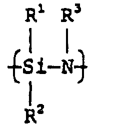
- The porous silica coating according to claim 5, wherein the content of Si, which exists in the form of a Si-R1 or Si-R2 bond, is within a range from 10 to 100 atomic % based on the number of Si atoms contained in the silica porous coating.
- The porous silica coating according to claim 6, wherein all of R1, R2 and R3 are hydrogen atoms.
- The porous silica coating according to claim 6 or 7, which is substantially free from a Si-N bond.
- A semiconductor device comprising the porous silica coating of claim 1 as an interlayer dielectric.
- A coating composition comprising an aluminum-containing polysilazane and a polyacrylate or polymethacrylate ester in an organic solvent.
Applications Claiming Priority (3)
| Application Number | Priority Date | Filing Date | Title |
|---|---|---|---|
| JP19928299 | 1999-07-13 | ||
| JP19928299A JP4408994B2 (en) | 1999-07-13 | 1999-07-13 | Low dielectric constant porous siliceous film, semiconductor device and coating composition |
| PCT/JP2000/004021 WO2001004049A1 (en) | 1999-07-13 | 2000-06-20 | Low-permittivity porous siliceous film, semiconductor devices having such films, and coating composition for forming the film |
Publications (3)
| Publication Number | Publication Date |
|---|---|
| EP1232998A1 true EP1232998A1 (en) | 2002-08-21 |
| EP1232998A4 EP1232998A4 (en) | 2002-10-16 |
| EP1232998B1 EP1232998B1 (en) | 2004-10-06 |
Family
ID=16405213
Family Applications (1)
| Application Number | Title | Priority Date | Filing Date |
|---|---|---|---|
| EP00937325A Expired - Lifetime EP1232998B1 (en) | 1999-07-13 | 2000-06-20 | Low-permittivity porous siliceous film, semiconductor devices having such films, and coating composition for forming the film |
Country Status (8)
| Country | Link |
|---|---|
| US (2) | US20030099843A1 (en) |
| EP (1) | EP1232998B1 (en) |
| JP (1) | JP4408994B2 (en) |
| KR (1) | KR100727277B1 (en) |
| CN (1) | CN1196649C (en) |
| DE (1) | DE60014694T2 (en) |
| TW (1) | TW593139B (en) |
| WO (1) | WO2001004049A1 (en) |
Cited By (1)
| Publication number | Priority date | Publication date | Assignee | Title |
|---|---|---|---|---|
| EP1321974A4 (en) * | 2000-08-29 | 2009-02-25 | Az Electronic Materials Usa | SILENT POROUS FILM WITH LOW PERMITTIVITY, SEMICONDUCTOR DEVICES AND COATING COMPOSITION |
Families Citing this family (22)
| Publication number | Priority date | Publication date | Assignee | Title |
|---|---|---|---|---|
| JP4574124B2 (en) * | 2003-05-01 | 2010-11-04 | Azエレクトロニックマテリアルズ株式会社 | Coating composition, porous siliceous film, method for producing porous siliceous film, and semiconductor device |
| JP4282493B2 (en) | 2004-01-15 | 2009-06-24 | 株式会社東芝 | Film forming method and substrate processing apparatus |
| JP2006054353A (en) * | 2004-08-13 | 2006-02-23 | Az Electronic Materials Kk | Siliceous film with little flat band shift and its production method |
| DE102005042944A1 (en) * | 2005-09-08 | 2007-03-22 | Clariant International Limited | Polysilazane-containing coatings for metal and polymer surfaces |
| DE102006008308A1 (en) * | 2006-02-23 | 2007-08-30 | Clariant International Limited | Coating preventing scale formation and corrosion on metal surfaces contains a linear and/or cyclic polysilazane, a solvent and a catalyst |
| JP2007242995A (en) * | 2006-03-10 | 2007-09-20 | Matsushita Electric Ind Co Ltd | Multilayer ceramic electronic component and manufacturing method thereof |
| JP2007273494A (en) * | 2006-03-30 | 2007-10-18 | Fujitsu Ltd | Insulating film forming composition and method for manufacturing semiconductor device |
| CN100444288C (en) * | 2006-07-21 | 2008-12-17 | 暨南大学 | Nanoporous polymethylsiloxane low dielectric constant material and its preparation method and application |
| WO2008102443A1 (en) * | 2007-02-21 | 2008-08-28 | Fujitsu Microelectronics Limited | Semiconductor device and process for producing the same |
| WO2008156680A1 (en) * | 2007-06-15 | 2008-12-24 | Sba Materials, Inc. | Low k dielectric |
| DE102009013904A1 (en) * | 2009-03-19 | 2010-09-23 | Clariant International Limited | Solar cells with an encapsulation layer based on polysilazane |
| DE102009013903A1 (en) | 2009-03-19 | 2010-09-23 | Clariant International Limited | Solar cells with a barrier layer based on polysilazane |
| JP5405437B2 (en) | 2010-11-05 | 2014-02-05 | AzエレクトロニックマテリアルズIp株式会社 | Method for forming isolation structure |
| JP5987514B2 (en) * | 2012-07-13 | 2016-09-07 | Dic株式会社 | Two-phase co-continuous silica structure and method for producing the same |
| CN104823265A (en) | 2012-10-31 | 2015-08-05 | Sba材料有限公司 | Compositions of low-K dielectric sols containing metal-free catalysts |
| WO2015005198A1 (en) * | 2013-07-08 | 2015-01-15 | コニカミノルタ株式会社 | Gas barrier film and electronic device |
| KR101497500B1 (en) * | 2014-06-16 | 2015-03-03 | 한국과학기술연구원 | Solar cell having wavelength converting layer and manufacturing method thereof |
| JP6929021B2 (en) * | 2016-04-25 | 2021-09-01 | Sppテクノロジーズ株式会社 | Method for manufacturing silicon oxide film |
| CN107022269B (en) * | 2017-04-10 | 2020-04-07 | 北京易净星科技有限公司 | Self-cleaning superhard polysilazane hydrophobic coating and preparation and use methods thereof |
| US20210095138A1 (en) * | 2019-09-27 | 2021-04-01 | B&B Blending, Llc | Use of a fluorescent optical brightener or phosphorescent indicator within ceramic coatings for visual detection and identification |
| CN113999584A (en) * | 2021-11-15 | 2022-02-01 | 长春中科应化特种材料有限公司 | Preparation method of anti-loosening marking paste containing polysilazane bolt |
| US20250336770A1 (en) * | 2023-10-18 | 2025-10-30 | Taiwan Semiconductor Manufacturing Company, Ltd. | Semiconductor device structure and methods of forming the same |
Family Cites Families (14)
| Publication number | Priority date | Publication date | Assignee | Title |
|---|---|---|---|---|
| US5032551A (en) * | 1988-03-05 | 1991-07-16 | Toa Nenryo Kogyo Kabushiki Kaisha | Silicon nitride based ceramic fibers, process of preparing same and composite material containing same |
| FR2694934B1 (en) * | 1992-08-24 | 1994-11-10 | Oreal | Composition for the treatment of acne containing a salicylic acid derivative and salicylic acid derivatives. |
| JP3414488B2 (en) * | 1994-04-28 | 2003-06-09 | 東燃ゼネラル石油株式会社 | Method for producing transparent organic / inorganic hybrid membrane |
| JPH09183949A (en) | 1995-12-28 | 1997-07-15 | Tonen Corp | Article coated with hard coat film and method for coating hard coat film |
| JPH10218690A (en) * | 1997-02-06 | 1998-08-18 | Kyocera Corp | Method for producing siliceous porous membrane |
| JP3939408B2 (en) * | 1997-09-30 | 2007-07-04 | Azエレクトロニックマテリアルズ株式会社 | Low dielectric constant siliceous film |
| JPH11105186A (en) * | 1997-09-30 | 1999-04-20 | Tonen Corp | Low dielectric constant siliceous film |
| JPH11105187A (en) * | 1997-09-30 | 1999-04-20 | Tonen Corp | Method for forming high-purity siliceous film and high-purity siliceous film |
| US6042994A (en) | 1998-01-20 | 2000-03-28 | Alliedsignal Inc. | Nanoporous silica dielectric films modified by electron beam exposure and having low dielectric constant and low water content |
| US6395651B1 (en) | 1998-07-07 | 2002-05-28 | Alliedsignal | Simplified process for producing nanoporous silica |
| US6090724A (en) | 1998-12-15 | 2000-07-18 | Lsi Logic Corporation | Method for composing a thermally conductive thin film having a low dielectric property |
| US6329017B1 (en) * | 1998-12-23 | 2001-12-11 | Battelle Memorial Institute | Mesoporous silica film from a solution containing a surfactant and methods of making same |
| US6413882B1 (en) * | 1999-04-14 | 2002-07-02 | Alliedsignal Inc. | Low dielectric foam dielectric formed from polymer decomposition |
| US6204202B1 (en) | 1999-04-14 | 2001-03-20 | Alliedsignal, Inc. | Low dielectric constant porous films |
-
1999
- 1999-07-13 JP JP19928299A patent/JP4408994B2/en not_active Expired - Fee Related
-
2000
- 2000-06-20 KR KR1020027000406A patent/KR100727277B1/en not_active Expired - Fee Related
- 2000-06-20 EP EP00937325A patent/EP1232998B1/en not_active Expired - Lifetime
- 2000-06-20 WO PCT/JP2000/004021 patent/WO2001004049A1/en not_active Ceased
- 2000-06-20 CN CNB008102120A patent/CN1196649C/en not_active Expired - Fee Related
- 2000-06-20 TW TW089112096A patent/TW593139B/en not_active IP Right Cessation
- 2000-06-20 DE DE60014694T patent/DE60014694T2/en not_active Expired - Lifetime
-
2001
- 2001-01-19 US US10/009,735 patent/US20030099843A1/en not_active Abandoned
-
2003
- 2003-02-24 US US10/370,588 patent/US6746714B2/en not_active Expired - Lifetime
Cited By (1)
| Publication number | Priority date | Publication date | Assignee | Title |
|---|---|---|---|---|
| EP1321974A4 (en) * | 2000-08-29 | 2009-02-25 | Az Electronic Materials Usa | SILENT POROUS FILM WITH LOW PERMITTIVITY, SEMICONDUCTOR DEVICES AND COATING COMPOSITION |
Also Published As
| Publication number | Publication date |
|---|---|
| EP1232998B1 (en) | 2004-10-06 |
| EP1232998A4 (en) | 2002-10-16 |
| KR100727277B1 (en) | 2007-06-13 |
| CN1360559A (en) | 2002-07-24 |
| TW593139B (en) | 2004-06-21 |
| US20030152783A1 (en) | 2003-08-14 |
| US20030099843A1 (en) | 2003-05-29 |
| DE60014694T2 (en) | 2005-10-27 |
| JP2001026415A (en) | 2001-01-30 |
| WO2001004049A1 (en) | 2001-01-18 |
| CN1196649C (en) | 2005-04-13 |
| DE60014694D1 (en) | 2004-11-11 |
| KR20020025191A (en) | 2002-04-03 |
| US6746714B2 (en) | 2004-06-08 |
| JP4408994B2 (en) | 2010-02-03 |
Similar Documents
| Publication | Publication Date | Title |
|---|---|---|
| EP1232998B1 (en) | Low-permittivity porous siliceous film, semiconductor devices having such films, and coating composition for forming the film | |
| EP1321974B1 (en) | Porous siliceous film having low permittivity, semiconductor devices and coating composition | |
| US6318124B1 (en) | Nanoporous silica treated with siloxane polymers for ULSI applications | |
| JP4947836B2 (en) | Polyfunctional Si-based oligomers and polymers, or nanoporous silica films for surface modification containing oligomers or polymers, processes for processing the same, and integrated circuits containing the same | |
| JP3888794B2 (en) | Method for forming porous film, wiring structure and method for forming the same | |
| US20020086166A1 (en) | Silane-based nanoporous silica thin films and precursors for making same | |
| JP2004312041A (en) | Low dielectric constant material and processing method by CVD | |
| EP0447611A2 (en) | Planarizing silsesquioxane copolymer coating | |
| JP2006500769A (en) | Interlayer adhesion promoter for low-k materials | |
| WO2004026765A1 (en) | Method for modifying porous film, modified porous film and use of same | |
| CN1836017B (en) | Coating composition and low dielectric siliceous material produced by using same | |
| JP2005503664A (en) | Electronic device and composition | |
| JP3939408B2 (en) | Low dielectric constant siliceous film | |
| JP2000077399A (en) | Silica-based porous membrane and method for producing the same | |
| JPH11105187A (en) | Method for forming high-purity siliceous film and high-purity siliceous film |
Legal Events
| Date | Code | Title | Description |
|---|---|---|---|
| PUAI | Public reference made under article 153(3) epc to a published international application that has entered the european phase |
Free format text: ORIGINAL CODE: 0009012 |
|
| 17P | Request for examination filed |
Effective date: 20020111 |
|
| AK | Designated contracting states |
Kind code of ref document: A1 Designated state(s): AT BE CH CY DE DK ES FI FR GB GR IE IT LI LU MC NL PT SE |
|
| A4 | Supplementary search report drawn up and despatched |
Effective date: 20020830 |
|
| AK | Designated contracting states |
Kind code of ref document: A4 Designated state(s): AT BE CH CY DE DK ES FI FR GB GR IE IT LI LU MC NL PT SE |
|
| RIC1 | Information provided on ipc code assigned before grant |
Free format text: 7C 09D 183/16 A, 7H 01L 21/312 B, 7C 01B 33/12 B |
|
| RAP1 | Party data changed (applicant data changed or rights of an application transferred) |
Owner name: CLARIANT INTERNATIONAL LTD. |
|
| GRAP | Despatch of communication of intention to grant a patent |
Free format text: ORIGINAL CODE: EPIDOSNIGR1 |
|
| RIN1 | Information on inventor provided before grant (corrected) |
Inventor name: AOKI, TOMOKO Inventor name: SHIMIZU, YASUO |
|
| GRAS | Grant fee paid |
Free format text: ORIGINAL CODE: EPIDOSNIGR3 |
|
| GRAA | (expected) grant |
Free format text: ORIGINAL CODE: 0009210 |
|
| AK | Designated contracting states |
Kind code of ref document: B1 Designated state(s): DE FR GB |
|
| REG | Reference to a national code |
Ref country code: GB Ref legal event code: FG4D |
|
| REG | Reference to a national code |
Ref country code: IE Ref legal event code: FG4D |
|
| REF | Corresponds to: |
Ref document number: 60014694 Country of ref document: DE Date of ref document: 20041111 Kind code of ref document: P |
|
| ET | Fr: translation filed | ||
| PLBE | No opposition filed within time limit |
Free format text: ORIGINAL CODE: 0009261 |
|
| STAA | Information on the status of an ep patent application or granted ep patent |
Free format text: STATUS: NO OPPOSITION FILED WITHIN TIME LIMIT |
|
| 26N | No opposition filed |
Effective date: 20050707 |
|
| REG | Reference to a national code |
Ref country code: GB Ref legal event code: 732E |
|
| REG | Reference to a national code |
Ref country code: FR Ref legal event code: TP |
|
| REG | Reference to a national code |
Ref country code: DE Ref legal event code: R082 Ref document number: 60014694 Country of ref document: DE Representative=s name: PATENTANWAELTE ISENBRUCK BOESL HOERSCHLER LLP, DE |
|
| REG | Reference to a national code |
Ref country code: GB Ref legal event code: 732E Free format text: REGISTERED BETWEEN 20150205 AND 20150211 |
|
| REG | Reference to a national code |
Ref country code: FR Ref legal event code: TP Owner name: MERCK PATENT GMBH, DE Effective date: 20150204 |
|
| REG | Reference to a national code |
Ref country code: DE Ref legal event code: R081 Ref document number: 60014694 Country of ref document: DE Owner name: MERCK PATENT GMBH, DE Free format text: FORMER OWNER: AZ ELECTRONIC MATERIALS USA CORP., SOMERVILLE, N.J., US Effective date: 20150223 Ref country code: DE Ref legal event code: R082 Ref document number: 60014694 Country of ref document: DE Representative=s name: PATENTANWAELTE ISENBRUCK BOESL HOERSCHLER LLP, DE Effective date: 20150223 |
|
| REG | Reference to a national code |
Ref country code: FR Ref legal event code: PLFP Year of fee payment: 17 |
|
| PGFP | Annual fee paid to national office [announced via postgrant information from national office to epo] |
Ref country code: DE Payment date: 20160614 Year of fee payment: 17 Ref country code: GB Payment date: 20160615 Year of fee payment: 17 |
|
| PGFP | Annual fee paid to national office [announced via postgrant information from national office to epo] |
Ref country code: FR Payment date: 20160516 Year of fee payment: 17 |
|
| REG | Reference to a national code |
Ref country code: DE Ref legal event code: R119 Ref document number: 60014694 Country of ref document: DE |
|
| GBPC | Gb: european patent ceased through non-payment of renewal fee |
Effective date: 20170620 |
|
| REG | Reference to a national code |
Ref country code: FR Ref legal event code: ST Effective date: 20180228 |
|
| PG25 | Lapsed in a contracting state [announced via postgrant information from national office to epo] |
Ref country code: GB Free format text: LAPSE BECAUSE OF NON-PAYMENT OF DUE FEES Effective date: 20170620 Ref country code: DE Free format text: LAPSE BECAUSE OF NON-PAYMENT OF DUE FEES Effective date: 20180103 |
|
| PG25 | Lapsed in a contracting state [announced via postgrant information from national office to epo] |
Ref country code: FR Free format text: LAPSE BECAUSE OF NON-PAYMENT OF DUE FEES Effective date: 20170630 |