Technical Field
-
The present invention relates to a ceramic heater used
principally in semiconductor industry.
Background Art
-
Semiconductors are very important products necessary in
various industries. Semiconductor chips are produced, for
example, by slicing a silicon monocrystal into a predetermined
thickness to produce a silicon wafer, and then forming a plurality
of integrated circuits and the like on the silicon wafer.
-
In a process for manufacturing such semiconductor chips,
a silicon wafer put on an electrostatic chuck is subjected to
various treatments such as etching, CVD and the like to form
a conductor circuit, an element and the like. Moreover, a resin
for a resist is applied and then is heated to dry.
-
For such heating, ceramic heaters are used, and heaters
in which carbide or nitride is used are disclosed in JP Kokai
Hei 11-74064, JP Kokai Hei 11-40330 and the like.
Summary of the Invention
-
However, the heater disclosed in JP Kokai Hei 11-74064
has a heating element embedded therein and has a problem that
the remaining heat cannot be cooled forcibly or the resistance
value of the heating element is not easily controlled.
-
The technology disclosed in JP Kokai Hei 11-40330 can solve
such problem since a resistance heating element is arranged
outside. However, there has been a problem: that a temperature
of the periphery of a heating face of a ceramic substrate becomes
lower than a set value; or that cracks are generated by rapid
temperature rising or rapid temperature falling.
-
The present invention was made in view of the
above-mentioned problem and an objective of the present invention
is to provide a heater in which: the residual heat of the heating
element can be easily cooled forcibly; the resistance value of
the heating element can be easily controlled; the temperature
of its periphery does not become lower than a set value; and
further, no cracks are generated due to rapid temperature rising
or rapid temperature falling.
-
The inventors of the present invention studied intensely
to achieve the above-mentioned objective and, as a result, they
have found that: the heater disclosed in JP Kokai Hei 11-74064
has an insulating ring being arranged in a peripheral portion
as shown in Fig. 1 of JP Kokai 2000-299281, thus a heating element
is not formed in the peripheral portion which is within
approximately 40 mm from the outer circumference thereof, and
therefore the temperature adjacent to the periphery falls and
the degree of thermal expansion in the vicinity of the periphery
differs from that in an inner portion due to the temperature
difference, resulting in generation of stress and generation
of cracks. They have reached the present invention through their
finding that forming a resistance heating element adjacent to
an outermost circumference of the ceramic substrate can prevent
such trouble.
-
That is, the present invention provides a ceramic heater
comprising a ceramic substrate which is principally in a disc
shape, and a resistance heating element formed on the surface
thereof,
wherein the outermost circumference of a resistance
heating element-formed area is located within 35 mm from the
side face of the ceramic substrate.
-
In the present invention, a resistance heating element
is formed on the surface of a ceramic substrate and therefore,
it is easy to measure a resistance value thereof and it is possible
to bring a cooling fluid directly into contact with the resistance
heating element when cooling the resistance heating element,
thereby to realize rapid temperature falling. Moreover, since
a heating face is formed in the opposite face to a resistance
heating element-formed face so that heat diffuses as the heat
is transmitted from the resistance-formed face to the heating
face. On the other hand, dissimilar to the case that a heating
element exists inside thereof, since the side face of the heating
element is not in contact with the ceramic substrate, the
temperature of the periphery easily falls. In the present
invention, the outermost circumference of a resistance heating
element-formed area is located within 35 mm from the side face
of the above-mentioned ceramic substrate, thus fall of the the
temperature of the periphery thereof is prevented by adopting
such a constitution. Moreover, since the temperature of the
periphery of the ceramic substrate does not fall, the generation
of cracks caused by rapid temperature rising and rapid
temperature falling can be prevented.
-
Furthermore, since a resistance heating element is formed
within 35 mm from the side face of the ceramic substrate, it
is not necessary to form an insulating ring, purposely.
-
Due to this, the fall of the peripheral temperature of
the ceramic substrate 11 can be prevented even if a ceramic
substrate is fixed with a supporting case (a casing) 51 through
a supporting pillar 56 in the manner that the ceramic substrate
is held with being in non-contact with the supporting case 51
as shown in Fig.3, thus the structure thereof can be simplified.
-
The above-mentioned ceramic substrate is desirably in a
disc shape. This is because such a disc shape is required to
have temperature evenness in its heating face, and therefore,
the constitution of the present invention can exhibit a great
effect.
-
The above-mentioned ceramic substrate desirably is a
carbide ceramic or a nitride ceramic. This is because these
are excellent in thermal conductivity.
-
The above-mentioned ceramic substrate desirably has a
thickness of 25 mm or less. This is because the heat of the
resistance heating element is easily conducted to the heating
face and, therefore, the temperature of the periphery does not
fall easily.
-
The diameter of the above-mentioned ceramic substrate
desirably exceeds 150 mm, and most desirably exceeds 210 mm.
This is because the temperature in the periphery easily falls
because the area of the heating face is large and, therefore,
the present invention can particularly exhibit its effect.
Brief Description of the Drawings
-
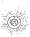
- Fig. 1 is a figure showing a pattern of a resistance heating
element of a ceramic heater of the present invention.
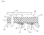
- Fig. 2 is a sectional view of a ceramic heater of the present
invention.
- Fig. 3 is a sectional view that illustrates an assembled
ceramic heater of the present invention.
| 10 | ceramic heater |
| 11 | ceramic substrate |
| 12 | resistance heating element |
| 13 | terminal pin |
| 14 | bottomed hole |
| 15 | through hole |
-
Detailed Disclosure of the Invention
-
The present invention will be described below in accordance
with embodiments thereof.
-
The present invention provides a ceramic heater comprising
a ceramic substrate which is principally in a disc shape, and
a resistance heating element formed on the surface thereof,
wherein the outermost circumference of a resistance
heating element-formed area is located within 35 mm from the
side face of the ceramic substrate.
-
In the ceramic heater according to this embodiment, a
nitride ceramic or a carbide ceramic is used as the ceramic
substrate and an oxide ceramic is used as an insulating layer
on the surface of the ceramic substrate. Incidentally, the
volume resistance value of a nitride ceramic easily drops at
a high temperature by the formation of solid solution of oxygen
and the like, and a carbide ceramic has conductivity unless it
is particularly highly purified. Thus, by forming an oxide
ceramic as an insulating layer, short circuit can be prevented
even at a high temperature or even if the carbide ceramic contains
impurities, so that the temperature controllability is secured.
-
The surface of the ceramic substrate preferably has a face
roughness of 0.05 to 20 µm in the value of Ra and 0.5 to 200
µm in the value of Rmax.
-
Examples of the nitride ceramic constituting the
above-mentioned ceramic substrate include metal nitride
ceramics such as aluminum nitride, silicon nitride, boron nitride,
titanium nitride and the like.
-
Examples of the above-mentioned carbide ceramic include
metal carbide ceramics such as silicon carbide, zirconium carbide,
titanium carbide, tantalum carbide, tungsten carbide and the
like.
-
As the ceramic substrate, an oxide ceramic may be used.
Thus, alumina, silica, cordierite, mullite, zirconia, beryllia
and the like can be used.
-
In the present invention, it is desired that the ceramic
substrate contains a sintering aid therein. Examples of the
sintering aid that can be used for aluminum nitride include alkali
metal oxides, alkali earth metal oxides or rare-earth oxides.
Particularly, CaO, Y2O3, Na2O, Li2O or Rb2O3 are preferable among
these sintering aids. Alumina can also be used. The content
of these sintering aids is desirably from 0.1 to 20% by weight.
-
In the case of silicon carbide, the sintering aid is
desirably B4C, C or AlN.
-
In the present invention, the ceramic substrate desirably
contains 5 to 5000 ppm of carbon therein.
-
This is because the incorporation of carbon can blacken
the ceramic substrate and it permits radiation heat to be
sufficiently utilized when the substrate is used as a heater.
-
The carbon may be either amorphous one or crystalline one.
This is because the use of amorphous carbon can prevent a drop
in a volume resistivity at a high temperature and the use of
crystalline carbon can prevent a drop in heat conductivity at
a high temperature. Accordingly, depending on the purpose of
use, both crystalline carbon and amorphous carbon may be used
together. The content of carbon is more preferably 50 to 2000
ppm.
-
The thickness of the ceramic substrate of the present
invention is desirably 50 mm or less, and especially desirably
25 mm or less.
-
If the thickness of the ceramic substrate exceeds 25 mm,
the heat capacity of the ceramic substrate becomes too large,
so that particularly when temperature control means is set up
to heat or cool the ceramic substrate, the temperature following
character may become poor due to the large heat capacity.
-
Particularly, the most suitable thickness is 5 mm or more.
The thickness desirably exceeds 1.5 mm.
-
The dispersion of the thickness of the ceramic substrate
is desirably within ±3%. The dispersion of the thermal
conductivity of the ceramic substrate is desirably within ±10%.
-
As the insulating layer used in the present invention,
an oxide ceramic is desirable. Specifically, silica, alumina,
mullite, cordierite, beryllia and so on can be used.
-
Such an insulating layer can be formed by spin-coating
a sol solution, which is prepared by hydrolyzing and polymerizing
an alkoxide, to the ceramic substrate, followed by drying and
firing the resultant. It may also be formed by sputtering, CVD
and the like. Moreover, an oxide layer may be formed by
subjecting the surface of a ceramic substrate to oxidation.
-
In the case of the ceramic heater of the present invention,
a semiconductor wafer may be put on the wafer-putting face of
the ceramic substrate so as to come in contact therewith. In
some cases, a semiconductor wafer is supported with a supporting
pin or a supporting ball to be held apart from the ceramic substrate
at a certain distance.
-
The distance thereof is desirably 5 to 5000 µm.
-
Regarding a semiconductor wafer, by moving the lifter pins
up and down, it is possible to receive the semiconductor wafer
from a carrier machine, put the semiconductor wafer on a ceramic
substrate, or heat the semiconductor wafer in the state that
the semiconductor wafer is supported.
-
The diameter of the ceramic substrate of the present
invention is desirably 200 mm or more. It is the most desirable
that the diameter is 12 inches (300 mm) or more. This is because
semiconductor wafers having such a diameter become a main stream
of the next-generation semiconductor wafers and also because
the temperature of the periphery easily falls, therefore the
constitution of the present invention is effective.
-
The outer shape of the above-mentioned ceramic substrate
is desirably equal to or larger than a semiconductor wafer.
Heating may be conducted while the ceramic substrate being kept
in non-contact with a semiconductor wafer.
-
The above-mentioned ceramic substrate desirably has
closed pores, and the leakage amount of helium is desirably 10-7
Pa·m3/sec or less. This is to prevent a coolant gas for forcible
cooling from leaking.
-
Furthermore, in order to secure the insulation between
resistance heating elements, it is desirable to adjust the volume
resistance of the ceramic substrate or the volume resistivity
of the insulating layer to 105 Ω·cm or more at a temperature
of 100°C or more.
-
It is advantageous that the flatness of the ceramic
substrate is 50 µm or less.
-
The ceramic heater of the present invention is used for
a device for producing or examining semiconductors. Examples
of specific devices include an electrostatic chuck, a wafer
prober, a susceptor and the like.
-
When the ceramic heater is used as an electrostatic chuck,
an electrostatic electrode and an RF electrode are formed in
addition to the resistance heating element and when it is used
as a wafer prober, a chuck top conductor layer as a conductor
is formed on its surface, and a guard electrode and a ground
electrode are formed as conductors inside the ceramic heater.
-
The ceramic substrate for semiconductor devices of the
present invention is desirably used at a temperature of 100 °C
or more, and most desirably at a temperature of 200 °C or more.
-
If necessary, in the present invention, a thermocouple
may be embedded in a bottomed hole in the ceramic substrate.
This is because the thermocouple makes it possible to measure
the temperature of the resistance heating element and, on the
basis of the measured data, voltage or electric current is changed
so that the temperature can be controlled.
-
The size of the connecting portions of metal wires of the
thermocouples is the same as or more than the strand diameter
of the respective metal wires, and is preferably 0.5 mm or less.
Such a structure reduces the heat capacity of the connecting
portion and causes a temperature to be correctly and rapidly
converted to a current value. For this reason, the temperature
controllability is improved so that the temperature distribution
in the heating face of a semiconductor wafer is reduced.
-
Examples of the above-mentioned thermocouple include K,
R, B, S, E, J and T type thermocouples as described in JIS-C-1602
(1980).
-
The temperature-measuring elements may be bonded to the
bottom of the bottomed hole 14 using gold solder, silver solder
and the like, or may be inserted into the bottomed hole and then
is sealed with a heat resistant resin. The both approaches may
be used together.
-
Examples of the above-mentioned heat resistant resin
include thermosetting resins, in particular, epoxy resins,
polyimide resins and bismaleimide-triazine resins. These
resins may be used alone or in combination of two or more.
-
The above-mentioned gold solder is desirably at least one
selected from an alloy of 37 to 80.5 % by weight of Au-63 to
19.5 % by weight of Cu and an alloy of 81.5 to 82.5 % by weight
of Au-18.5 to 17.5 % by weight of Ni. This is because these
have a melting temperature of 900 °C or more and are not easily
melted even in a high temperature range.
-
As the silver solder, for example, an Ag-Cu type one can
be used.
-
As shown in Fig. 1, the heating element 12 is desirably
divided into at least two circuits, and more desirably divided
into 2 to 10 circuits. By dividing a circuit, each electric
power supplied to the respective circuits can be controlled to
change the calorific value thereof so that the temperature of
the wafer heating face 11a can be adjusted.
-
Examples of the pattern of the heating element 12 include
spirals and eccentric circles as well as the pattern comprising
a combination of concentric circles-like and a winding line as
shown in Fig. 1.
-
In the present invention, an insulating layer is formed
before the formation of the heating element. The insulating
layer can be formed by the spin-coating of a sol solution, which
is prepared by hydrolyzing and polymerizing an alkoxide, to the
surface of a ceramic substrate, followed by the drying and firing
of the resultant, or by sputtering, CVD and the like. Moreover,
an oxide layer may be formed by the firing of the surface of
a ceramic substrate in an oxidizing atmosphere.
-
In case that the heating element is formed on the surface
of the ceramic substrate 11, a preferable method is one comprising
steps of : applying a conductor containing paste containing metal
particles to the surface of the ceramic substrate 11 to form
a conductor containing paste layer with a predetermined pattern;
and then firing the conductor containing paste layer to sinter
the metal particles on the surface of the ceramic substrate 11.
If the metal particles are fused and adhered to each other and
the metal particles and the ceramic are fused and adhered to
each other in the sintering of the metal, the sintering is
sufficient.
-
In this embodiment, a pattern like that shown in Fig. 1
is adopted. In the ceramic substrate 11, there exist 12d as
a resistance heating element-formed area 1, 12c as a resistance
heating element-formed area 2, 12b as a resistance heating
element-formed area 3 and 12a as a resistance heating
element-formed area 4. Also, buffering areas of resistance
heating element-formed areas are formed between the resistance
heating element-formed area 1 and the resistance heating
element-formed area 2, between the resistance heating
element-formed area 2 and the resistance heating element-formed
area 3, and between the resistance heating element-formed area
3 and the resistance heating element-formed area 4. Because
of the existence of these buffering areas, the rise of the
temperature caused by the application of large electric power
to the resistance heating element-formed area 2 gives no
influence to the resistance heating element-formed area 1 or
the resistance heating element-formed area 3. Thus, there is
no necessity of temperature control, such as causing the
temperature of the resistance heating element-formed area 1 or
the resistance heating element-formed area 3 to fall. Thus,
the temperature difference in the heating face can be reduced
by simple control.
-
The outermost circumference of the resistance heating
element-formed areas must be located within 35 mm from the side
face of the above-mentioned ceramic substrate, and the most
desirably within 25 mm. This is because if within 25 mm, the
warp amount can be extremely small.
-
Furthermore, it is desirable to set the distance between
the outermost circumference of the resistance heating
element-formed areas and the side face of the above-mentioned
ceramic substrate to be 0.5 mm or more. This is because if the
distance is less than 0.5 mm, electric short circuit will occur
or the handling property will be deteriorated in case that a
supporting case is made of metal.
-
In the ceramic heater according to this embodiment, the
width of the resistance heating element-formed areas is adjusted
to 5 to 30% of the diameter thereof.
-
In the ceramic substrate 11, a through hole 15 is formed
and a lifter pin is inserted in it.
-
The face roughness of the through hole is desirably 0.05
to 200 µm in the value of Rmax and 0.005 to 20 µm in the value
of Ra.
-
In a bottomed hole 14, a temperature-measuring device is
formed. On the resistance heating element 12, a terminal portion
13 is formed thereon.
-
As the resistance heating element-formed areas, a
concentric, spiral, or winding pattern is formed. It is
desirable that one resistance heating element-formed area has
one circuit. This is because a resistance heating
element-formed area with one circuit is easier to be controlled.
-
When the heating element is formed on the surface of the
ceramic substrate 11, the thickness of the heating element 12
is preferably 1 to 30 µm and more preferably 1 to 10 µm.
-
When the heating element is formed on the surface of the
ceramic substrate 11, the width of the heating element is
preferably 0.1 to 20 mm and more preferably 0.1 to 5 mm.
-
The resistance value of the heating element 12 can be
changed depending on its width or thickness. The
above-mentioned ranges are however most practical. The
resistance value becomes larger as the heating element becomes
thinner and narrower.
-
By setting the position where the heating element is formed
in such a manner, the heat generated from the heating element
is diffused throughout the ceramic substrate during the
transmission of the heat, resulting in the evenness of the
temperature distribution of the face where an object to be heated
(a silicon wafer) will be heated. As a result, the temperature
of every portion of the object to be heated will become even.
-
The heating element may have a rectangular section or an
elliptical section. It desirably has a flat section. This is
because: in case of the flat section, heat is more easily radiated
toward the wafer heating face. Thus, a temperature distribution
on the wafer heating face is not easily generated.
-
The aspect ratio (the width of the heating element/the
thickness of the heating element) of the section is desirably
10 to 5000.
-
Adjustment thereof into this range makes it possible to
increase the resistance value of the heating element 12 and secure
the evenness of the temperature on the wafer heating face.
-
In case that the thickness of the heating element 12 is
made constant: if the aspect ratio is smaller than the
above-mentioned range, the amount of heat conduction toward the
wafer heating face of the ceramic substrate 11 becomes small
so that a thermal distribution similar to the pattern of the
heating element is generated on the wafer heating face; on the
other hand, if the aspect ratio is too large, the temperature
of the portions just above the middle line of the heating element
becomes high so that a thermal distribution similar to the pattern
of the heating element is also generated on the wafer heating
face. Accordingly, if temperature distribution is considered,
the aspect ratio of the section is preferably 10 to 5000.
-
When the heating element is formed on the surface of the
substrate 11, the aspect ratio is desirably 10 to 200. When
the heating element is formed inside the substrate 11, the aspect
ratio is desirably 200 to 5000.
-
The aspect ratio becomes larger in case that the heating
element is formed inside the substrate 11. This is because if
the heating element is formed inside, the distance between the
wafer heating face and the heating element becomes short and,
therefore, the temperature evenness of the surface is
deteriorated, this resulting in the necessity of flattening the
heating element itself.
-
The conductor containing paste is not particularly limited,
and is preferably a paste comprising not only metal particles
or a conductive ceramic for keeping electrical conductivity but
also a resin, a solvent, a thickener and the like.
-
The above-mentioned metal particles are preferably of,
for example, a noble metal (gold, silver, platinum and palladium) ,
lead, tungsten, molybdenum, nickel and the like. These may be
used alone or in combination of two or more. This is because
these metals are not relatively easily oxidized and have a
sufficient resistance value to generate heat.
-
Examples of the above-mentioned conductive ceramic
include carbides of tungsten, molybdenum and the like. These
may be used alone or in combination of two or more.
-
The particle diameter of these metal particles or the
conductive ceramic is preferably 0.1 to 100 µm. If the particle
diameter is too fine, that is, less than 0.1 µm, they are easily
oxidized. On the other hand, if the particle diameter exceeds
100 µm, they are not easily sintered so that the resistance value
becomes large.
-
The shape of the above-mentioned metal particles may be
spherical or scaly. When these metal particles are used, they
may be a mixture of spherical particles and scaly particles.
-
In case that the above-mentioned metal particles are scaly
or a mixture of spherical particles and scaly particles, metal
oxides between the metal particles are easily retained and
adhesion between the heating element and the nitride ceramic
and the like is made sure. Moreover, the resistance value can
be made large. Thus, these cases are profitable.
-
Examples of the resin used in the conductor containing
paste include epoxy resins, phenol resins and the like . Examples
of the solvent are isopropyl alcohol and the like. Examples
of the thickener are cellulose and the like.
-
As for the conductor containing paste, it is desirable
that metal oxide is added to metal particles so that the heating
element is composed of a material prepared by sintering the metal
particles and the metal oxide. By sintering the metal oxide
together with the metal particles in this way, nitride ceramic
or carbide ceramic, which is a ceramic substrate, can be firmly
adhered to the metal particles.
-
The reason why the adhesion to the nitride ceramic or
carbide ceramic is improved by mixing the metal oxide is unclear ,
but would be based on the following. The surface of the metal
particles or the surface of the nitride ceramic or carbide ceramic
is slightly oxidized so that oxidized films are formed thereon.
The oxidized films are sintered to integrate through a metal
oxide, and as a result, the metal particles are adhered firmly
to the nitride ceramic or the carbide ceramic.
-
Preferred examples of the above-mentioned metal oxide
include at least one selected from the group consisting of lead
oxide, zinc oxide, silica, boron oxide (B2O3), alumina, yttria
and titania.
-
These oxides make it possible to improve adhesion between
the metal particles and the nitride ceramic or the carbide ceramic
without increasing the resistance value of the heating element.
-
When the total amount of the metal oxides is set to 100
parts by weight, the weight ratios of the above-mentioned lead
oxide, zinc oxide, silica, boron oxide (B2O3), alumina, yttria
and titania are as follows: lead oxide: 1 to 10, silica: 1 to
30, boron oxide: 5 to 50, zinc oxide: 20 to 70, alumina: 1 to
10, yttria: 1 to 50 and titania: 1 to 50. The weight ratios
are preferably adjusted within the range that the total thereof
does not exceed 100 parts by weight.
-
By adjusting the amounts of these oxides within those
ranges, the adhesion to the nitride ceramic can be particularly
improved.
-
The addition amount of the above-mentioned metal oxides
to the metal particles is preferably 0.1 % by weight or more
and less than 10 % by weight. The area resistivity achieved
when the conductor containing paste having such a composition
is used to form the heating element is preferably from 1 to 45
mΩ/□.
-
This is because if the area resistivity exceeds 45 mΩ/□,
the amount of heat generated to the applied voltage becomes too
small so that, in the ceramic substrate 11 wherein a heating
element is formed on its surface, the amount of the heat generated
is not easily controlled. If the addition amount of the metal
oxides is 10% by weight or more, the area resistivity exceeds
50 mΩ/□ so that the amount of the heat generated becomes too
small. Thus, temperature control is not easily performed so
that the evenness in temperature distribution is deteriorated.
-
In case that the heating element is formed on the surface
of the substrate 11, a metal covering layer (reference to Fig.
2) 120 is desirably formed on the surface portion of the heating
element. This is because the metal covering layer prevents a
change in the resistance value due to the oxidization of the
internal metal sintered body. The thickness of the metal
covering layer 120 to be formed is preferably from 0.1 to 10
µm.
-
The metal to be used for forming the metal covering layer
120 is not particularly limited if the metal is a metal which
is hardly oxidized. Specific examples thereof include gold,
silver, palladium, platinum, nickel and the like. These may
be used alone or in combination of two or more. Among these
metals, nickel is preferred.
-
In the heating element, a terminal for connecting it to
a power source is necessary. This terminal is fixed to the
heating element through a solder. Therein, Nickel prevents a
solder from being thermally diffused. An example of the
connecting terminal is a terminal pin 13 made of Koval.
-
In case that the connecting terminal is connected, an alloy
such as silver-lead, lead-tin or bismuth-tin can be used as a
solder. The thickness of the solder layer is desirably from
0.1 to 50 µm. This is because this range is a range sufficient
for securing the connection by the solder.
-
Next, a description will be made to a manufacturing process
of a ceramic heater of the present invention.
-
The following will describe a manufacturing process of
a ceramic heater 10 wherein a heating element is formed inside
a ceramic substrate (reference to Fig. 2).
(1) Step of forming a ceramic heater
-
A slurry is prepared by blending powder made of the
above-mentioned nitride ceramic or carbide ceramic with a
sintering aid such as yttria, a binder and so on, based on the
necessity. Thereafter, this slurry is made into a granular form
by spray drying and the like. The granule is put into a mold
and is pressed to form into a plate form and the like. Thus,
a raw formed body (green) is prepared.
-
Next, a portion that will become a through hole 15 into
which a supporting pin for supporting a silicon wafer is inserted;
and a portion that will become a bottomed hole 14 in which a
temperature measuring element such as a thermocouple is embedded:
are formed in the raw formed body, if necessary.
-
Next, this raw formed body is heated and is fired for
sintering. Thus, aplate-formed body made of ceramic is produced.
Thereafter, the plate-formed body is made into a predetermined
shape to produce a substrate 11. The raw formed body may have
such a shape that it can be used as it is after firing. Heating
and firing the raw formed body under pressure can produce a
substrate 11 free from pores. It is sufficient that the heating
and the firing are performed at the sintering temperature or
more. The firing temperature is 1000 to 2500 °C for nitride
ceramic or carbide ceramic. It is to be noted that the through
hole, the bottomed hole and so on may be formed after the production
of the sintered body.
(2) Step of printing a conductor containing paste on a substrate
-
A conductor containing paste is generally a fluid
comprising metal particles, a resin and a solvent and having
a high viscosity. This conductor containing paste is printed,
by screen printing and the like, in the portion where a heating
element is to be arranged to form a conductor containing paste
layer. Since it is necessary that the heating element makes
the temperature of the whole of the substrate even, the conductor
containing paste is desirably printed into a pattern comprising
a combination of concentric circles-like and winding lines as
shown in Fig. 1.
-
The conductor containing paste layer is desirably formed
in the manner that a section of the heating element 12 after
firing is rectangular and flat. The conductor containing paste
layer must be formed so that the outermost circumference of the
resistance heating element-formed area of the ceramic substrate
to be obtained is located within 35 mm from the side face of
the ceramic substrate.
(3) Firing of a conductor containing paste
-
The conductor containing paste layer printed on the bottom
face of the substrate is heated and is fired to remove the resin
and the solvent, and the metal particles are sintered. Thus,
the metal particles are baked onto the bottom face of the substrate
11 to form the heating element 12. The heating and firing
temperature is preferably 500 to 1000 °C.
-
If the above-mentioned metal oxides are added to the
conductor containing paste, the metal particles, the substrate
and the metal oxides are sintered to integrate with each other.
Thus, the adhesion between the heating element 12 and the
substrate 11 is improved.
(4) Step of forming a metal covering layer
-
A metal covering layer is desirably formed on the surface
of the heating element 12. The metal covering layer can be formed
by electroplating, electroless plating, sputtering and the like.
From the viewpoint of mass-productivity, electroless plating
is most suitable.
(5) Attaching of terminals, etc.
-
A terminal (a terminal pin 13) for connecting to a power
source is attached to an end of the pattern of the heating element
12 with a solder. A thermocouple is fixed to the bottomed hole
14 with a silver solder, a gold solder and the like. The bottomed
hole 14 is sealed with a heat resistant resin such as a polyimide
to finish the manufacture of the ceramic heater 10.
-
The ceramic heater of the present invention may be provided
with an electrostatic electrode to be used as an electrostatic
chuck, and also may be provided with a chuck top conductor layer
to be used as a wafer prober.
-
An assembled structure of this ceramic heater is shown
in Fig. 3.
-
In this ceramic heater 10, a resistance heating element
12 is formed on a ceramic substrate 11. The face opposing the
face on which the resistance heating element is formed is a wafer
heating face 11a. The ceramic heater 10 is fixed to a supporting
case (a casing) 51 through a supporting pillar 56. Thus, there
is no insulating ring. In the present invention, the falling
of the temperature of the peripheral portion thereof can be
inhibited without any insulating ring. The ceramic substrate
11 is in non-contact with the supporting case 51. A fixing metal
member 56a is attached to the supporting pillar 56. Furthermore,
a through hole 150 through which a lifter pin is inserted is
formed in the ceramic substrate 11. A power-supplying terminal
54 is fixed to the resistance heating element through a spring
55. Furthermore, an intermediate bottom plate 52 and a bottom
plate 51a are fixed to the supporting case 51. An opening 510
is formed on the bottom plate 51a. The intermediate bottom plate
52 is fixed in a space inside the supporting case 51 with a spring
53. The bottom plate 51a is provided with a cooling nozzle 59.
Cooling is conducted by blowing the air and the like. Moreover,
a thermocouple 44 for temperature controlling is pressed on the
bottom plate 51a with a spring 45 through a heat transfering
plate 42.
-
Best Mode for Carrying out the Invention
(Example 1) Production of a ceramic heater made of SiC (reference
to FIGS. 1, 2)
- (1) A composition made of 100 parts by weight of SiC powder
(average particle diameter: 0.3 µm), 4 parts by weight of a
sintering aid, that is B4C, 12 parts by weight of an acrylic
binder and an alcohol was subjected to spray-drying to form
granular powder.
- (2) Next, this granular powder was put into a mold and was
formed into a flat plate form to obtain a raw formed body (green) .
- (3) The raw formed body subjected to the above-mentioned
treatment was hot-pressed at 2100 °C and a pressure of 18 MPa
to obtain a ceramic plate made of SiC having a thickness of 3
mm.
Next, this plate-formed body was cut into a disc having
a diameter of 210 mm and was ground into a mirror plane until
its surface has an Ra value of 0.1 µm, thus to obtain a ceramic
substrate 11.A film of SiO2 having a thickness of 2 µm was formed on
the surface of the ceramic substrate 11 made of SiC by applying
a sol solution which is prepared by hydrolyzing and polymerizing
a mixed solution composed of 25 parts by weight of tetraethyl
silicate, 37.6 parts by weight of ethanol and 0.3 part by weight
of hydrochloric acid for 24 hours under stirring, to the ceramic
substrate 11 by spin-coating, followed by drying it at 80 °C
for 5 hours, then followed by firing it at 1000 °C for 1 hour.The resulting formed body was subjected to drilling to
form a portion that would become a through hole 15 into which
a supporting pin for a silicon wafer is inserted and a portion
(diameter: 1.1 mm, depth: 2 mm) that would become a bottomed
hole 14 in which a thermocouple is embedded.
- (4) A conductor containing paste was printed, by screen
printing, on the ceramic substrate 11 obtained in the step (3).
The pattern of the printing was a pattern of a combination of
concentric circles-like and winding lines as shown in Fig. 1.
Incidentally, the outermost circumference of the
resistance heating element-formed area was located 30 mm apart
from the side face of the above-mentioned ceramic substrate.The used conductor containing paste was Solvest PS603D
made by Tokuriki Kagaku Kenkyusho Co., which is used to form
plated through holes in printed circuit boards. This conductor containing paste was a silver paste and
contained 7.5 parts by weight of metal oxides comprising lead
oxide (5% by weight), zinc oxide (55% by weight), silica (10%
by weight) , boron oxide (25% by weight) and alumina (5% by weight)
per 100 parts by weight of silver. The silver particles had
an average particle diameter of 4.5 µm and were scaly.
- (5) Next, the ceramic substrate 11 on which the conductor
containing paste was printed was heated and fired at 780 °C to
sinter silver in the conductor containing paste and bake it onto
the substrate 11. Thus, a heating element 12 was formed. The
silver heating element 12 had a thickness of 5 µm, a width of
2.4 mm and an area resistivity of 7.7 mΩ/□.
- (6) The substrate 11 prepared in the step (5) was immersed
into an electroless nickel plating bath comprising an aqueous
solution containing 80 g/L of nickel sulfate, 24 g/L of sodium
hypophosphite, 12 g/L of sodium acetate, 8 g/L of boric acid,
and 6 g/L of ammonium chloride to precipitate a metal covering
layer (nickel layer) 120 having a thickness of 1 µm on the surface
of the silver-lead heating elements 12.
- (7) By screen printing, a silver-lead solder paste (made by
Tanaka Kikinzoku Kogyo Co.) was printed on the portion to which
a terminal for securing connection to a power source would be
attached, to form a solder layer.
Next, a terminal pin 13 made of Koval was mounted on the
solder layer and was heated for reflowing at 420 °C. Thus, the
terminal 13 was attached to the surface of the heating element
12.
- (8) A thermocouple for controlling temperature was fitted into
the bottomed hole 14 and a ceramic adhesive (ARON CERAMIC, made
by TOAGOSEI Co., LTD.) was embedded thereinto. Thus, a ceramic
heater 10 was obtained.
-
(Example 2)
-
The operation was conducted according to Example 1, but
the outermost circumference of the resistance heating
element-formed area was located 20 mm apart from the side face
of the above-mentioned ceramic substrate.
(Example 3)
-
The operation was conducted according to Example 1, but
the outermost circumference of the resistance heating
element-formed area was located 10 mm apart from the side face
of the above-mentioned ceramic substrate.
(Example 4)
-
The operation was conducted according to Example 1, but
the outermost circumference of the resistance heating
element-formed area was located 1 mm apart from the side face
of the above-mentioned ceramic substrate.
(Comparative example 1)
-
The operation was conducted in the same manner as Example
1, but the outermost circumference of the resistance heating
element-formed area was located 40 mm apart from the side face
of the above-mentioned ceramic substrate.
(Example 5) Production of a ceramic heater made of aluminum
nitride (reference to FIGS. 1, 2)
-
- (1) A composition made of 100 parts by weight of aluminum
nitride powder (average particle diameter: 0.6 µm), 4 parts by
weight of yttria (average particle diameter: 0.4 µm), 12 parts
by weight of an acrylic binder and an alcohol was subjected to
spray-drying to form granular powder.
- (2) Next, this granular powder was put into a mold and was
formed into a flat plate-form to obtain a raw formed body (green) .
- (3) The raw formed body subjected to the above-mentioned
treatment was hot-pressed at 1800 °C and a pressure of 20 MPa
to obtain an aluminum nitride plate-formed body having a
thickness of 3 mm.
Next, this plate-formed body was cut into a disc having
a diameter of 210 mm to form a ceramic substrate 11. To the
surface of this substrate, the sol solution mentioned in Example
1 was applied and then was dried. The resultant was fired to
form a SiO2 film having a thickness of 2 µm.This formed body was subjected to drilling to form a portion
which would become a through hole 15 into which a supporting
pin for a silicon wafer is inserted and a portion (diameter:
1.1 mm, depth: 2 mm) which would become a bottomed hole 14 in
which a thermocouple is embedded.
- (4) A conductor containing paste was printed, by screen
printing, on the substrate 11 obtained in the step (3). The
pattern of the printing was a pattern of a combination of
concentric circles-like and winding lines as shown in Fig. 1.
Incidentally, the outermost circumference of the
resistance heating element-formed area was located 30 mm apart
from the side face of the above-mentioned ceramic substrate.The used conductor containing paste was Solvest PS603D
made by Tokuriki Kagaku Kenkyusho Co., which is used to form
plated through holes in printed circuit boards.This conductor containing paste was a silver-lead paste
and contained 7.5 parts by weight of metal oxides comprising
lead oxide (5% by weight) , zinc oxide (55% by weight) , silica
(10% by weight), boron oxide (25% by weight) and alumina (5%
by weight) per 100 parts by weight of silver. The silver
particles had an average particle diameter of 4.5 µm and were
scaly.
- (5) Next, the substrate 11 on which the conductor containing
paste was printed was heated and fired at 780 °C to sinter silver
in the conductor containing paste and bake it onto the substrate
11. Thus, a heating element 12 was formed. The heating element
12 had a thickness of 5 µm, a width of 2.4 mm and an area resistivity
of 7.7 mΩ/□.
- (6) The substrate 11 prepared in the step (5) was immersed
into an electroless nickel plating bath comprising an aqueous
solution containing 80 g/L of nickel sulfate, 24 g/L of sodium
hypophosphite, 12 g/L of sodium acetate, 8 g/L of boric acid,
and 6 g/L of ammonium chloride to precipitate a metal covering
layer (nickel layer) 120 having a thickness of 1 µm on the surface
of the silver-lead heating elements 12.
- (7) By screen printing, a silver-lead solder paste (made by
Tanaka Kikinzoku Kogyo Co.) was printed on the portion to which
a terminal for securing connection to a power source would be
attached, to form a solder layer. Next, a terminal pin 13 made
of Koval was mounted on the solder layer and was heated for
reflowing at 420 °C. Thus, the terminal 13 was attached to the
surface of the heating element 12.
- (8) A thermocouple for controlling temperature was fitted into
the bottomed hole 14 and a ceramic adhesive (ARON CERAMIC, made
by TOAGOSEI Co., LTD.) was embedded thereinto. Thus, a ceramic
heater 10 was obtained.
-
(Example 6)
-
The operation was conducted according to Example 5, but
the outermost circumference of the resistance heating
element-formed area was located 20 mm apart from the side face
of the above-mentioned ceramic substrate.
(Example 7)
-
The operation was conducted according to Example 5, but
the outermost circumference of the resistance heating
element-formed area was located 10 mm apart from the side face
of the above-mentioned ceramic substrate.
(Example 8)
-
The operation was conducted according to Example 5, but
the outermost circumference of the resistance heating
element-formed area was located 1 mm apart from the side face
of the above-mentioned ceramic substrate.
(Comparative example 2)
-
The operation was conducted in the same manner as Example
8, but the outermost circumference of the resistance heating
element-formed area was located 40 mm apart from the side face
of the above-mentioned ceramic substrate.
-
This comparative example was conducted according to the
manufacturing method of a ceramic heater disclosed in JP Kokai
Hei 11-40330. In this heater, as shown in Fig. 1 of JP Kokai
2000-299281, an insulating ring is disposed in the peripheral
portion, and therefore, there is no heating element in the
peripheral portion.
(Comparative example 3)
-
- (1) A green sheet having a thickness of 0.47 µm was obtained
through the formation by the doctor blade method using a paste
obtained by mixing 100 parts by weight of aluminum nitride powder
(made by Tokuyama Corp., average particle diameter: 1.1 µm),
4 parts by weight of yttria (average particle diameter: 0.4 µm),
11.5 parts by weight of an acrylic binder, 0.5 part by weight
of a dispersant and 53 parts by weight of an alcohol comprising
1-butanol and ethanol.
- (2) Next, this green sheet was dried at 80 °C for 5 hours,
and was subjected to punching to form portions which would become
through holes 15 having diameters of 1.8 mm, 3.0 mm and 5.0 mm,
respectively, into which semiconductor wafer supporting pins
are inserted and portions which would become conductor-filled
through holes for connection to external terminals.
- (3) A conductor containing paste A was prepared by mixing 100
parts by weight of tungsten carbide particles having an average
particle diameter of 1 µm, 3.0 parts by weight of an acrylic
binder, 3.5 parts by weight of α-terpineol solvent and 0.3 part
by weight of a dispersant.
A conductor containing paste B was prepared by mixing 100
parts by weight of tungsten particles having an average particle
diameter of 3 µm, 1.9 parts by weight of an acrylic binder, 3.7
parts by weight of α-terpineol solvent and 0.2 part by weight
of a dispersant.This conductor containing paste A was printed on the green
sheet by screen printing to form a conductor containing paste
layer for a resistance heating element. The pattern of the
printing was a concentric pattern.Furthermore, the conductor containing paste B was filled
into the through holes for the formation of conductor-filled
through holes for connecting external terminals.On the green sheet that had been subjected to the
above-mentioned processing, thirty four green sheets having no
tungsten paste printed were stacked on (on the heating face of)
the green sheet 50, and thirteen sheets of the same green sheets
having no tungsten paste printed were stacked under the green
sheet 50. Furthermore, a green sheet 50 having a printed
conductor containing paste layer having an electrostatic
electrode pattern was stacked thereon. Furthermore, two green
sheets 50' having no tungsten paste printed were stacked thereon.
The resultant was pressed at 130 °C and a pressure of 8 MPa to
form a lamination.
- (4) Next, the resultant lamination was degreased at 600 °C
in the atmosphere of nitrogen gas for 5 hours and hot-pressed
at 1890 °C and a pressure of 15 MPa for 3 hours to obtain an
aluminum nitride plate-formed body of 3 mm in thickness. This
was cut into a disc having 230 mm in diameter to form a ceramic
substrate made of aluminum nitride that had a resistance heating
element having a thickness of 6 µm and a width of 10 mm inside.
The resistance heating element inside the ceramic substrate was
disposed in a manner that the outermost circumference of the
resistance heating element-formed area was located 30 mm apart
from the side face of the above-mentioned ceramic substrate.
- (5) Next, the plate-formed body obtained in the step of (4)
was ground with a diamond grindstone. Subsequently, a mask was
mounted thereon, and bottomed holes (diameter: 1.2 mm, depth:
2.0 mm) for fitting thermocouples were formed in the surface
by blast treatment with SiC and the like.
- (6) Furthermore, portions where the conductor-filled through
holes were formed were hollowed out to form blind holes. To
the blind holes, external terminals made of Koval were connected
by heating and reflowing at 700 °C using brazing gold comprising
Ni-Au.
As for the connection of the external terminals, a
structure wherein a support of tungsten supports at three points
is desirable. This is because the reliability of the connection
can be secured.
- (7) Next, thermocouples for controlling temperature were
embedded in the bottomed holes.
-
(Example 9) Production of a ceramic heater made of SiC
-
- (1) A composition made of 100 parts by weight of SiC powder
(average particle diameter: 0.3 µm), 4 parts by weight of a
sintering aid, that is B4C, 12 parts by weight of an acrylic
binder and an alcohol was subjected to spray-drying to form
granular powder.
- (2) Next, this granular powder was put into a mold and was
formed into a flat plate form to obtain a raw formed body (green) .
- (3) The raw formed body subjected to the above-mentioned
treatment was hot-pressed at 2100 °C and a pressure of 18 MPa
to obtain an SiC ceramic plate having a thickness of 3 mm.
Next, this plate-formed body was cut into a disc having
a diameter of 310 mm and was mirror-ground until its surface
has an Ra value of 0.1 µm, thus to obtain a ceramic substrate
11.A film of SiO2 having a thickness of 2 µm was formed on
the surface of the ceramic substrate 11 made of SiC by applying
a sol solution prepared by hydrolyzing and polymerizing a mixed
solution composed of 25 parts by weight of tetraethyl silicate,
37.6 parts by weight of ethanol and 0.3 part by weight of
hydrochloric acid for 24 hours under stirring, to the ceramic
substrate 11 by spin-coating, followed by drying it at 80 °C
for 5 hours, then followed by firing it at 1000 °C for 1 hour.The resulting formed body was subjected to drilling to
form a portion that would become a through hole 15 into which
a supporting pin for a silicon wafer is inserted and a portion
(diameter: 1.1 mm, depth: 2 mm) that would become a bottomed
hole 14 in which a thermocouple is embedded.
- (4) A conductor containing paste was printed, by screen
printing, on the ceramic substrate 11 obtained in the step (3).
The pattern of the printing was a pattern of a combination of
concentric circles-like and winding lines as shown in Fig. 1.
Incidentally, the outermost circumference of the
resistance heating element-formed area was located 0.5 mm apart
from the side face of the above-mentioned ceramic substrate.The used conductor containing paste was Solvest PS603D
made by Tokuriki Kagaku Kenkyusho Co., which is used to form
plated through holes in printed circuit boards.This conductor containing paste was a silver paste and
contained 7.5 parts by weight of metal oxides comprising lead
oxide (5% by weight) , zinc oxide (55% by weight), silica (10%
by weight) , boron oxide (25% by weight) and alumina (5% by weight)
per 100 parts by weight of silver. The silver particles had
an average particle diameter of 4.5 µm and were scaly.
- (5) Next, the ceramic substrate 11 on which the conductor
containing paste was printed was heated and fired at 780 °C to
sinter silver in the conductor containing paste and bake it onto
the substrate 11. Thus, a heating element 12 was formed. The
silver heating element 12 had a thickness of 5 µm, a width of
2.4 mm and an area resistivity of 7.7 mΩ/□.
- (6) The substrate 11 prepared in the step (5) was immersed
into an electroless nickel plating bath comprising an aqueous
solution containing 80 g/L of nickel sulfate, 24 g/L of sodium
hypophosphite, 12 g/L of sodium acetate, 8 g/L of boric acid,
and 6 g/L of ammonium chloride to precipitate a metal covering
layer (nickel layer) having a thickness of 1 µm on the surface
of the silver-lead heating elements 12.
- (7) By screen printing, a silver-lead solder paste (made by
Tanaka Kikinzoku Kogyo Co.) was printed on the portion to which
a terminal for securing connection to a power source would be
attached, to form a solder layer.
Next, a terminal pin 13 made of Koval was mounted on the
solder layer and was heated for reflowing at 420 °C. Thus, the
terminal 13 was attached to the surface of the heating element
12.
- (8) Athermocouple for controlling temperature was fitted into
the bottomed hole 14 and a ceramic adhesive (ARON CERAMIC, made
by TOAGOSEI Co., LTD.) was embedded thereinto. Thus, a ceramic
heater was obtained.
-
(Example 10)
-
The operation was conducted in the same manner as Example
9, but the outermost circumference of the resistance heating
element-formed area was located 35 mm apart from the side face
of the above-mentioned ceramic substrate.
(Comparative example 4)
-
The operation was conducted in the same manner as
Comparative example 3, but the distance from the outermost
circumference of the resistance heating element-formed area to
the side face of the ceramic substrate was set to 40 mm.
(Comparative example 5)
-
The operation was conducted in the same manner as Example
9, but the outermost circumference of the resistance heating
element-formed area was located 40 mm apart from the side face
of the above-mentioned ceramic substrate. This comparative
example is according to JP Kokai Hei 11-40330. In this heater,
as shown in Fig. 1 of JP Kokai 2000-299281, an insulating ring
is disposed in the peripheral portion, and therefore, there is
no heating element in the peripheral portion.
(Comparative example 6)
-
The operation was conducted in the same manner as Example
1, but the diameter of the ceramic substrate was set to 150 mm
and the outermost circumference of the resistance heating
element-formed area was located 40 mm apart from the side face
of the above-mentioned ceramic substrate.
(Comparative example 7)
-
The operation was conducted in the same manner as Example
9, but the outermost circumference of the resistance heating
element-formed area was located 0.2 mm apart from the side face
of the above-mentioned ceramic substrate. When an electric
current was passed in the heating element, the discharge from
the heating element to the supporting case occurred.
-
Furthermore, each of the heaters of the Examples and the
Comparative examples was assembled into a supporting case as
shown in Fig. 3 to form a unit and was heated to 400 °C. The
temperature difference between the periphery and the inner
portion was measured using a thermoviewer (IR-16-2012-0012,
manufactured by Japan Datum Co., Ltd.) Moreover, the
temperature was raised to 400 °C over 45 seconds and the incidence
of cracks was examined. Furthermore, the temperature-falling
time was measured by performing forcible cooling from 200 °C
to 150 °C by blowing the air.
-
The results are shown in Table 1.
| | Distance between the outer circumference of a resistance heating element and the outer circumference of a ceramic substrate (mm) | Temperature difference (°C) | Cracks (%) | Temperature-falling time (min.) |
| Example 1 | 30 | 4 | 0 | 2 |
| Example 2 | 20 | 4 | 0 | 2 |
| Example 3 | 10 | 3 | 0 | 2 |
| Example 4 | 1 | 3 | 0 | 2 |
| Example 5 | 30 | 4 | 0 | 2 |
| Example 6 | 20 | 4 | 0 | 2 |
| Example 7 | 10 | 4 | 0 | 2 |
| Example 8 | 1 | 3 | 0 | 2 |
| Example 9 | 0.5 | 2 | 0 | 2 |
| Example 10 | 35 | 4 | 0 | 2 |
| Comparative example 1 | 40 | 8 | 4 | 2 |
| Comparative example 2 | 40 | 8 | 4 | 2 |
| Comparative example 3 | 30 | 4 | 0 | 10 |
| Comparative example 4 | 40 | 4 | 4 | 10 |
| Comparative example 5 | 40 | 12 | 7 | 2 |
| Comparative example 6 | 40 | 5 | 2 | 2 |
| Comparative example 7 | 0.2 | - | - | - |
-
As is clear from the results shown in Table 1, a cooling
time can be shortened by forming a resistance heating element
on a surface. Moreover, the formation of a resistance heating
element on a surface makes the temperature difference in a heating
surface large (from a comparison of Comparative examples 2 and
4). The forming of a resistance heating element within 35 mm
from the side face of a ceramic substrate makes the temperature
difference in a heating face small. In addition, no crack is
formed even by rapid temperature rising (from a comparison
between Examples 1 to 10 and Comparative examples).
-
Moreover, a comparison of Comparative example 1 and
Comparative example 5 shows that a ceramic substrate with a larger
diameter gives a larger temperature difference.
-
Furthermore, a comparison of Comparative Example 1 and
Comparative example 6 shows that a ceramic substrate with a
smaller diameter gives a smaller temperature difference.
-
The present invention has solved the problem of falling
of peripheral temperature observed in large ceramic heaters
having diameters exceeding 150 mm. The effect of the present
invention is remarkable when a ceramic heater has a diameter
exceeding 210 mm.
Industrial Applicability
-
As described above, according to the present invention,
a heater can be realized, in which: it is easy to forcibly cool
remaining heat in a heating element; it is easy to control the
resistance value of the heating element; the temperature of the
periphery of the heater does not become lower than a set value;
and no cracks are generated by rapid temperature rising or rapid
temperature falling.