EP1231801A2 - Wireless communication apparatus processing intermittent data - Google Patents
Wireless communication apparatus processing intermittent data Download PDFInfo
- Publication number
- EP1231801A2 EP1231801A2 EP01113086A EP01113086A EP1231801A2 EP 1231801 A2 EP1231801 A2 EP 1231801A2 EP 01113086 A EP01113086 A EP 01113086A EP 01113086 A EP01113086 A EP 01113086A EP 1231801 A2 EP1231801 A2 EP 1231801A2
- Authority
- EP
- European Patent Office
- Prior art keywords
- signal processing
- signal
- clock
- control
- power source
- Prior art date
- Legal status (The legal status is an assumption and is not a legal conclusion. Google has not performed a legal analysis and makes no representation as to the accuracy of the status listed.)
- Granted
Links
Images


Classifications
-
- H—ELECTRICITY
- H04—ELECTRIC COMMUNICATION TECHNIQUE
- H04W—WIRELESS COMMUNICATION NETWORKS
- H04W52/00—Power management, e.g. TPC [Transmission Power Control], power saving or power classes
- H04W52/02—Power saving arrangements
- H04W52/0209—Power saving arrangements in terminal devices
- H04W52/0225—Power saving arrangements in terminal devices using monitoring of external events, e.g. the presence of a signal
- H04W52/0229—Power saving arrangements in terminal devices using monitoring of external events, e.g. the presence of a signal where the received signal is a wanted signal
-
- H—ELECTRICITY
- H04—ELECTRIC COMMUNICATION TECHNIQUE
- H04W—WIRELESS COMMUNICATION NETWORKS
- H04W52/00—Power management, e.g. TPC [Transmission Power Control], power saving or power classes
- H04W52/02—Power saving arrangements
-
- H—ELECTRICITY
- H04—ELECTRIC COMMUNICATION TECHNIQUE
- H04W—WIRELESS COMMUNICATION NETWORKS
- H04W52/00—Power management, e.g. TPC [Transmission Power Control], power saving or power classes
- H04W52/02—Power saving arrangements
- H04W52/0209—Power saving arrangements in terminal devices
- H04W52/0261—Power saving arrangements in terminal devices managing power supply demand, e.g. depending on battery level
- H04W52/0274—Power saving arrangements in terminal devices managing power supply demand, e.g. depending on battery level by switching on or off the equipment or parts thereof
- H04W52/028—Power saving arrangements in terminal devices managing power supply demand, e.g. depending on battery level by switching on or off the equipment or parts thereof switching on or off only a part of the equipment circuit blocks
- H04W52/0283—Power saving arrangements in terminal devices managing power supply demand, e.g. depending on battery level by switching on or off the equipment or parts thereof switching on or off only a part of the equipment circuit blocks with sequential power up or power down of successive circuit blocks, e.g. switching on the local oscillator before RF or mixer stages
-
- Y—GENERAL TAGGING OF NEW TECHNOLOGICAL DEVELOPMENTS; GENERAL TAGGING OF CROSS-SECTIONAL TECHNOLOGIES SPANNING OVER SEVERAL SECTIONS OF THE IPC; TECHNICAL SUBJECTS COVERED BY FORMER USPC CROSS-REFERENCE ART COLLECTIONS [XRACs] AND DIGESTS
- Y02—TECHNOLOGIES OR APPLICATIONS FOR MITIGATION OR ADAPTATION AGAINST CLIMATE CHANGE
- Y02D—CLIMATE CHANGE MITIGATION TECHNOLOGIES IN INFORMATION AND COMMUNICATION TECHNOLOGIES [ICT], I.E. INFORMATION AND COMMUNICATION TECHNOLOGIES AIMING AT THE REDUCTION OF THEIR OWN ENERGY USE
- Y02D30/00—Reducing energy consumption in communication networks
- Y02D30/70—Reducing energy consumption in communication networks in wireless communication networks
Definitions
- the present invention relates to a wireless communication apparatus processing intermittent data, and more particularly, to the structure of a data processing part for processing a base band signal in a wireless communication apparatus for receiving/transmitting intermittent data such as packet data.
- the present invention is suitable to communication terminal equipment used for processing packet data which is used for a mobile communication system of a CDMA (Code Division Multiple Access) method, etc.
- a wireless communication apparatus for processing a signal mainly on software has been devised corresponding to the variation and complication of wireless communication methods.
- a wireless communication apparatus shown in FIG. 11 is disclosed in, for example, a magazine of "Nikkei Electronics” published by Nikkei Business Publications, Inc., No. 732, pp.183-193.
- IF intermediate frequency
- RF radio frequency
- the inputted IF signal is converted into a digital signal by an A/D converter 33, then, is quadrature-demodulated by a half-band filter (HBF) 34, and is converted into an I-signal and a Q-signal.
- the I- and Q- signals are stored in a memory 35.
- DSP digital signal processor
- the DSP 36 transmits the processed signal to a central processing unit (hereinlater, abbreviated to a CPU) 37 as received data.
- the CPU 37 performs processes for upper layers such as call control operation, and outputs the processed output to the outside via external interface.
- a clock generator 38 supplies a clock signal necessary for the above-described components.
- the communication is not always performed in the packet data communication, and it is known that the period in which no packet data is received/transmitted is long.
- TSG RAN SWG1 TS25.211 (3rd Generation Partnership Project; Technical Specification Group Radio Access Network; Physical channels and mapping of transport channels onto physical channels (FDD) (3G TS TS25.211 version 2.2.1) prescribes that a down signal to be transmitted to a terminal from a base station is communicated with a frame structure shown in FIGS. 9A to 9C.
- the signal is structured by sequentially linking frames.
- one frame comprises fifteen slots.
- FIG. 9B one frame comprises fifteen slots.
- one slot comprises a DPCCH data portion having control data (Pilot, TFCI, and TPC) and a DPDCH data portion in which user data (Data1 and Data2) is stored.
- the user data is transmitted only when the packet exists, and in cases except therefor, the transmission of the user data suspends.
- 3GPP TSG_RAN_WG1 TS25.214-v1.1.1 as shown in FIG. 10, if there is no downlink transmitting data to a terminal from a base station, the transmission of the DPDCH data portion suspends and only the DPCCH data portion is transmitted.
- the base station starts the transmission of the DPCCH data portion and the transmission of dummy DPDCH data portion, and the transmission of downlink DPDCH data portion in which the user data is stored resumes.
- the transmission and suspension of the user data are repeated in the packet data communication and, therefore, it is considered that the amount of processed signals to be averagely obtained is relatively small.
- the DSP in the conventional wireless communication apparatus needs to always supply a clock signal corresponding to a communication signal process at the maximum communication data rate and the power consumption cannot be effectively reduced if the amount of processed signals decreases.
- a wireless communication apparatus having a wireless processing part for processing a wireless signal including intermittent data such as packet data and a data processing part for receiving/transmitting the intermittent data to/from the wireless processing part, wherein the data processing part includes a plurality of signal processing blocks whose signal processing periods are different such as a symbol, slot, and frame of signal processing units, a buffer memory which is provided between the plurality of signal processing blocks, a clock control part which supplies a clock signal to each of the plurality of signal processing blocks and the buffer memory, and a power source control part which supplies a power source to each of the plurality of signal processing blocks and the buffer memory.
- At least one of the plurality of signal processing blocks has means for watching which watches whether or not there is data to be processed in the subsequent signal processing block having a different processing period.
- the clock control part has means for controlling an operation to supply or suspend the clock signal to the subsequent signal processing block based on the watched result of the means for watching.
- the wireless communication apparatus further has means for controlling a power voltage to be supplied to the signal processing block and a memory block based on the watched result of the means for watching.
- the present invention by independently supplying the clock signals to a plurality of signal processing engines having different processing periods and independently controlling the power voltages, power consumption can be effectively reduced in an intermittent transmitting sequence of packet data because powers of an operating signal processing circuit and a memory can be decreased.
- FIG. 1 shows the construction of a mobile communication system in which a wireless communication apparatus of the present invention is used.
- a plurality of base stations 1 and 2 perform wireless communication among a plurality of wireless communication apparatuses (mobile terminals) 3, 4, and 5.
- the base stations 1 and 2 are connected to a network 7 via a base station control center 6.
- the base stations 1 and 2 have predetermined communicable areas 8 and 9, thus performing communication with the mobile terminals 3 and 4 in the areas 8 and 9, respectively.
- FIG. 2 shows one construction of the mobile terminals 3, 4, and 5, etc.
- Each of the mobile terminals 3, 4, and 5 has an antenna 10 which receives/transmits a wireless signal between the base stations 1 and 2 and the mobile terminals 3, 4, and 5, a base band signal processing part 12 which is connected to the antenna 10 via a radio frequency circuit 11, and a data processing part 13 which is connected to the base band signal processing part 12 and processes user data.
- the base band signal processing part 12 demodulates a received signal to be supplied from the radio frequency circuit 11, decodes it, and transmits it to the data processing part 13 for processing the user data. Transmitting data from the data processing part 13 is encoded, is subjected to a modulation, and is supplied to the radio frequency circuit 11.
- the data processing part 13 comprises a processor 14, a memory 15, various peripherals 16, a display device 18, and a key pad 17, etc., which are connected via a bus line 19, and also performs conversion between a signal received/transmitted in a wireless manner and a signal to be received/transmitted to/from a user, etc.
- FIG. 3 shows the construction of the base band signal processing part 12 in the wireless communication apparatus according to one embodiment of the present invention.
- the present embodiment shows the base band signal processing part which processes the signal of the frame structure mentioned in FIGS. 9A to 9C, and the base band signal processing part 12 comprises one large scale integrated (LSI) circuit.
- the received base band signal which is supplied from the radio frequency circuit 11 is stored in a buffer memory 21.
- the received signal stored in the buffer memory 21 is subjected to a synchronizing process and a spectrum despreading process, etc. by a symbol period processing engine 22, thereby converting the signal into a signal based on a symbol unit.
- the signal based on the symbol unit is stored in a buffer memory 23.
- a slot period processing engine 24 performs processes such as detection and Rake combining, and stores the signals in a buffer memory 25.
- a frame period processing engine 26 performs processes such as de-interleave and error correction, and outputs the signals as received data to the data processing part 13.
- transmitting data to be supplied from the data processing part 13 is subjected to processes such as error correction encoding, interleave, modulation, spectrum spread by a transmitting signal processing engine 29, and the processed transmitting-signal is outputted to the radio frequency circuit 11.
- the symbol period processing engine 22 and the slot period processing engine 24 as signal processing engines watch whether or not there is data to be processed by the slot period processing engine 24 and the frame period processing engine 26 as the individual subsequent signal processing engines.
- a control engine 20 controls operations of the symbol period processing engine 22, slot period processing engine 24, frame period processing engine 26, and transmitting signal processing engine 29 as the signal processing engines, thereby issuing an instruction to subsequently perform the above-mentioned signal processing.
- the control engine 20 supplies a clock signal only for a period in which the symbol period processing engine 22, slot period processing engine 24, frame period processing engine 26, and transmitting signal processing engine 29 are to be operated. For a period except therefor, the control engine 20 controls a clock control part 28 to suspend the clock signal. Also, based on the watched result, the control engine 20 controls a power source control part 27 to reduce power consumption for a period in which the symbol period processing engine 22, slot period processing engine 24, frame period processing engine 26, and transmitting signal processing engine 29, and the buffer memories 21, 23, and 25 are not operated. To be specific, the control engine 20 decreases a power voltage for a period in which the operation is unnecessary and generates a specific bias voltage to diminish a leak current of the memory, etc.
- FIG. 4 shows the construction of the symbol period processing engine 22 as the signal processing engine. Although FIG. 4 also shows the construction of the symbol period processing engine 22 and the buffer memories 21 and 23 on the input/output side thereof, the same construction as the foregoing is applied to that of the slot period processing engine 24 and the buffer memories 23 and 24 on the input/output side thereof and that of the frame period processing engine 26 and the buffer memory 25 on the input side thereof.
- the symbol period processing engine 22 as the signal processing engine reads out the signal stored in the buffer memory 21.
- the read-out signal is subjected to a signal process by a simplified processor 30 and an auxiliary hardware 31 for processing the read-out signal.
- the processed result is stored in the buffer memory 23.
- the signal processing engine 22 has an internal memory (RAM) 32 which stores parameters, etc. necessary for temporary storage of the processed result and operations.
- the simplified processor 30 d-controls the operation with the symbol period processing engine 22 in accordance with an instruction of the control engine 20, executes a signal process necessary for the symbol period processing engine 22 in collaboration with the auxiliary hardware 31, and transmits various measured results, watched result, and operating processing state to the control engine 20.
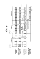
- FIG. 5 is a time chart showing an example of the operational sequence when no user data DPDCH is transmitted in the received signal in the wireless communication apparatus according to the embodiment of the present invention.
- horizontal-line portions, oblique-line portions, and vertical-line portions indicate that there is valid data.
- FIG. 5 indicates that in the received signals, there is valid data in the user data DPCCH and DPDCH in a frame 1 and, on the contrary, there is valid data only in the user data DPCCH and no valid data in the user data DPDCH in frames 2 and 3.
- the symbol period processing engine 22, slot period processing engine 24, and frame period processing engine 27 continuously operate.
- the symbol period processing engine 22 watches whether or not there is valid data in the user data DPDCH in the received signals in the slot portion at the head of the frame.
- the control engine 20 controls the clock control part 28 and the power source control part 27 so that the symbol period processing engine 22 operates only during one slot period at the head of the frame and during reception of the DPCCH data. Also, the control engine 20 controls the operation so that the slot period processing engine 24 operates only during one slot period at the head of the frame and during reception of the DPCCH. Further, the control engine 20 controls an operation to suspend so that the frame period processing engine 26 is suspended after the frame process which is currently being processed is finished. Thereafter, the symbol period processing engine 22 intermittently continues a process of the DPCCH while watching the resumption of the DPDCH data portion or the suspension of the DPCCH data portion in the head slots of the subsequent frames to frame 3.
- FIG. 6 is a time chart showing an example of the operational sequence in the case of change from a state in which there is only the DPCCH data portion in the received signals to the frame in which the DPDCH resumes in the wireless communication apparatus according to the embodiment of the present invention.
- the symbol period processing engine 22 watches the resumption of the DPDCH data portion and the suspension of the DPCCH data portion in the slot at the head of the frame while processing the DPCCH data portion in a period (frame 4) in which there is not DPDCH data portion. As the watched result, if the resumption of the DPDCH data portion is detected as indicated in a frame 5, the symbol period processing engine 22 transmits the watched result to the control engine 20.
- the control engine 20 controls the clock control part 28 and the power source control part 27 so that, subsequently thereto, the symbol period processing engine 22 and the slot period processing engine 24 operate continuously. Also, the control engine 20 controls the resumption of operation of the frame period processing engine 26 (frame 6), thus executing a decoding process of the resumed user data. Subsequently thereto, the symbol period processing engine 22, slot period processing engine 24, and frame period processing engine 26 as the signal processing engines operate continuously for a period in which there is DPDCH data portion in the slot at the head of the frame.
- FIG. 7 is a time chart showing an example of the operational sequence in the case of change from a state in which there is only the DPCCH data portion in the received signals to the frame in which the DPCCH suspends in the wireless communication apparatus according to the embodiment of the present invention.
- the symbol period processing engine 22 watches the resumption of the DPDCH data portion and the suspension of the DPCCH data portion in the slot at the head of the frame while intermittently executing a process for the DPCCH data portion. As the watched result, if the suspension (non-existence) of the DPCCH data portion is detected at the head of the frame as indicated in a frame 8, the symbol period processing engine 22 transmits the watched result to the control engine 20.
- the control engine 20 controls the clock control part 28 and the power source control part 27 based on the watched result so that, subsequently thereto, the symbol period processing engine 22 operates only during the period of the DPCCH data portion at the head of the frame and the slot period processing engine 24 suspends the operation subsequent to the next slot. After that, the symbol period processing engine 22 operates only for a period of the DPCCH data portion in the slot at the head of the frame and watches the resumption of the DPCCH data portion as indicated in a frame 9.
- FIG. 8 is a time chart showing an example of the operational sequence in the case of change from a state in which the received signal is completely suspended to a state in which the DPCCH and DPDCH data portions resume in the wireless communication apparatus according to the embodiment of the present invention.
- the symbol period processing engine 22 operates for the period of the DPCCH data portion in the slot at the head of the frame and watches the resumption of the DPCCH data portion.
- the control engine 20 controls the clock control part 28 and the power source control part 27 so that, subsequently thereto, the symbol period processing engine 22 operates for a period over the frame 10, the slot period processing engine 24 continuously operates for a period of slots subsequent to the second slot in the frame 10, and the frame period processing engine 26 continuously operates for a period of data subsequent to a frame 11.
- a decoding process of the resumed user data is performed. After that, the symbol period processing engine 22, slot period processing engine 24, and frame period processing engine 26 continuously operate.
- the number of operating signal processing circuits can be minimized in the intermittent transmitting sequence of the packet data which is prescribed in FIG. 10, thereby effectively reducing power consumption.
- the present invention is not limited to the above embodiment and can be embodied to a wireless communication apparatus for intermittently communicating data. It is unnecessary to control clock signals and power sources of all plural signal processing blocks having different processing functions, and it is possible to control the clock signal and power source of the main signal processing block.
Abstract
Description
Claims (8)
- A wireless communication apparatus having a wireless processing part for processing a wireless signal including intermittent data and a base band signal processing part for receiving/transmitting said intermittent data to/from said wireless processing part, wherein said base band signal processing part comprises:a plurality of signal processing blocks having different signal processing periods;a buffer memory which is provided between said plurality of signal processing blocks;a clock control part which supplies a clock signal to each of said plurality of signal processing blocks and said buffer memory;a power source control part which supplies a power source to each of said plurality of signal processing parts and said buffer memory; anda control engine which controls said plurality of signal processing blocks, said buffer memory, said clock control part, and said power source control part, andat least one of said plurality of signal processing blocks has means for watching which watches whether or not there is data to be processed in the subsequent signal processing block having the different signal processing period, andsaid control engine also controls said clock control part to supply or suspend the clock signal to said subsequent signal processing block based on a watched result of said means for watching.
- A wireless communication apparatus according to Claim 1, wherein said control engine further controls said power source control part to supply the power source to be supplied to said subsequent signal processing block based on said watched result.
- A wireless communication apparatus according to Claim 1, wherein said intermittent data comprises a signal with a signal format including a periodic control data portion and a user data portion, and is a signal that a control signal is periodically transmitted when there is not said user data portion, andsaid at least one of signal processing blocks watches the existence of said user data portion and, when there is not said user data portion as the watched result, said control engine controls said clock control part to supply or suspend the clock signal to said at least one of signal processing blocks over a period in which said user data portion is to be processed.
- A wireless communication apparatus according to Claim 3, wherein said control engine further has means for controlling said power source control part to control the power source to be supplied to said subsequent signal processing block based on said watched result.
- A wireless communication apparatus according to Claim 1, wherein said intermittent data comprises a signal with a signal format including a periodic control data portion and a user data portion, is a signal that a control signal is periodically transmitted when there is not user data portion, and is a signal to suspend said periodic control data portion when there is not said user data portion sequentially a predetermined times or more, andsaid control engine controls said clock control part to supply or suspend the clock signal for a period in which the control signal is to be processed to at least one of said plurality of signal processing blocks based on said watched result.
- A wireless communication apparatus according to Claim 5, wherein said control engine further controls said power source part to control the power source to be supplied to said subsequent signal processing block based on said watched result.
- A large scale integrated circuit comprising:a plurality of signal processing blocks having different signal processing periods;a buffer memory which is provided between said plurality of signal processing blocks;a clock control part which supplies a clock signal to each of said plurality of signal processing blocks and said buffer memory;a power source control part which supplies a power source to each of said plurality of signal processing blocks and said buffer memory; anda control engine which controls said plurality of signal processing blocks, said buffer memory, said clock control part, and said power source control part, whereinat least one of said plurality of signal processing blocks has means for watching which watches whether or not there is data to be processed in the subsequent signal processing block having the different processing period, and said control engine has means for controlling said clock control part to supply or suspend the clock signal to said subsequent signal processing block based on a watched result of said means for watching.
- A large scale integrated circuit according to Claim 7, wherein said plurality of signal processing blocks having the different signal processing periods has: a signal processing block which processes data based on a symbol unit; a signal processing block which processes data based on a slot unit; and a signal processing block which processes data based on a frame unit.
Applications Claiming Priority (2)
| Application Number | Priority Date | Filing Date | Title |
|---|---|---|---|
| JP2001033392 | 2001-02-09 | ||
| JP2001033392A JP3819242B2 (en) | 2001-02-09 | 2001-02-09 | Wireless communication device that handles intermittent signals |
Publications (3)
| Publication Number | Publication Date |
|---|---|
| EP1231801A2 true EP1231801A2 (en) | 2002-08-14 |
| EP1231801A3 EP1231801A3 (en) | 2003-08-27 |
| EP1231801B1 EP1231801B1 (en) | 2009-12-30 |
Family
ID=18897148
Family Applications (1)
| Application Number | Title | Priority Date | Filing Date |
|---|---|---|---|
| EP20010113086 Expired - Lifetime EP1231801B1 (en) | 2001-02-09 | 2001-05-29 | Wireless communication apparatus processing intermittent data |
Country Status (6)
| Country | Link |
|---|---|
| US (1) | US6807235B2 (en) |
| EP (1) | EP1231801B1 (en) |
| JP (1) | JP3819242B2 (en) |
| KR (1) | KR100730258B1 (en) |
| DE (1) | DE60140930D1 (en) |
| TW (1) | TW561731B (en) |
Families Citing this family (30)
| Publication number | Priority date | Publication date | Assignee | Title |
|---|---|---|---|---|
| US6993669B2 (en) * | 2001-04-18 | 2006-01-31 | Gallitzin Allegheny Llc | Low power clocking systems and methods |
| US6990598B2 (en) * | 2001-03-21 | 2006-01-24 | Gallitzin Allegheny Llc | Low power reconfigurable systems and methods |
| KR100402786B1 (en) * | 2001-07-30 | 2003-10-22 | 한국전자통신연구원 | Apparatus for TFCI Mapping in Wireless Communication Mobile Station and Method Thereof |
| US7502817B2 (en) * | 2001-10-26 | 2009-03-10 | Qualcomm Incorporated | Method and apparatus for partitioning memory in a telecommunication device |
| US7269448B2 (en) * | 2001-11-09 | 2007-09-11 | Electronics And Telecommunications Research Institute | Method for recognizing request for data transmission by mobile/base station RRC using network transfer device |
| US6907028B2 (en) * | 2002-02-14 | 2005-06-14 | Nokia Corporation | Clock-based time slicing |
| US7130313B2 (en) * | 2002-02-14 | 2006-10-31 | Nokia Corporation | Time-slice signaling for broadband digital broadcasting |
| WO2004088927A1 (en) * | 2003-03-27 | 2004-10-14 | Matsushita Electric Industrial Co., Ltd. | Intermittent communication method and intermittent communication device |
| US7478260B2 (en) * | 2003-10-20 | 2009-01-13 | Hewlett-Packard Development Company, L.P. | System and method for setting a clock rate in a memory card |
| US9112620B2 (en) * | 2005-03-10 | 2015-08-18 | Qualcomm Incorporated | Method of enabling power savings when no data is being transmitted on a media logical channel |
| US20060259807A1 (en) * | 2005-05-10 | 2006-11-16 | Telairity Semiconductor, Inc. | Method and apparatus for clock synchronization between a processor and external devices |
| JP4513974B2 (en) * | 2005-06-27 | 2010-07-28 | 日本電気株式会社 | Wireless communication network that broadcasts high-priority information, method for changing the same, and wireless communication network design tool |
| JP2007095040A (en) * | 2005-08-31 | 2007-04-12 | Matsushita Electric Ind Co Ltd | Data processing apparatus, program, recording medium, and content playback apparatus |
| US20070124395A1 (en) * | 2005-09-22 | 2007-05-31 | Stephen Edge | Geography-based filtering of broadcasts |
| JP4509945B2 (en) * | 2006-02-08 | 2010-07-21 | 富士通株式会社 | Device heat generation control device in data transfer device |
| TWI316374B (en) * | 2006-07-21 | 2009-10-21 | Hon Hai Prec Ind Co Ltd | System and method for saving power of station |
| US7620833B2 (en) * | 2006-12-04 | 2009-11-17 | Intel Corporation | Power saving for isochronous data streams in a computer system |
| US7916676B2 (en) * | 2007-03-23 | 2011-03-29 | Broadcom Corporation | Method and system for holistic energy management in ethernet networks |
| US8849183B2 (en) | 2007-10-05 | 2014-09-30 | Qualcomm Incorporated | Location and time based filtering of broadcast information |
| JP4962396B2 (en) * | 2008-04-23 | 2012-06-27 | 日本電気株式会社 | Packet processing device |
| JP5007703B2 (en) * | 2008-05-19 | 2012-08-22 | 日本電気株式会社 | Packet processing apparatus, packet control method, and packet control program |
| US9280778B2 (en) | 2008-12-15 | 2016-03-08 | Qualcomm Incorporated | Location logging and location and time based filtering |
| US8374091B2 (en) * | 2009-03-26 | 2013-02-12 | Empire Technology Development Llc | TCP extension and variants for handling heterogeneous applications |
| US9996102B2 (en) * | 2010-07-20 | 2018-06-12 | Nxp Usa, Inc. | Clock circuit and method for providing an electronic device with an adjustable clock signal |
| KR20120018266A (en) | 2010-08-20 | 2012-03-02 | 삼성전자주식회사 | Method and apparatus for controlling power amplifier consumption power of base station in wireless communication system using orthogonal frequency division multiple access |
| US9485108B2 (en) | 2011-03-14 | 2016-11-01 | Qualcomm Incorporated | System and apparatus for using multichannel file delivery over unidirectional transport (“FLUTE”) protocol for delivering different classes of files in a broadcast network |
| US9451401B2 (en) | 2011-05-27 | 2016-09-20 | Qualcomm Incorporated | Application transport level location filtering of internet protocol multicast content delivery |
| KR200457848Y1 (en) * | 2011-08-19 | 2012-01-05 | 이호상 | Bed for medicine hospital |
| US9310873B2 (en) * | 2012-08-31 | 2016-04-12 | Vixs Systems, Inc. | Video processing device with register adjustment generator and methods for use therewith |
| WO2020069203A1 (en) | 2018-09-26 | 2020-04-02 | Intel Corporation | Frequency generation and synchronization systems and methods |
Citations (1)
| Publication number | Priority date | Publication date | Assignee | Title |
|---|---|---|---|---|
| EP0655872A2 (en) | 1993-11-26 | 1995-05-31 | Nokia Mobile Phones Ltd. | Paging message processing |
Family Cites Families (5)
| Publication number | Priority date | Publication date | Assignee | Title |
|---|---|---|---|---|
| JPH01190054A (en) | 1988-01-25 | 1989-07-31 | Man Design Kk | Receiver |
| WO1996003811A1 (en) | 1994-07-21 | 1996-02-08 | Interdigital Technology Corporation | Power consumption control method and apparatus for a communication system subscriber unit |
| ATE205616T1 (en) * | 1994-10-19 | 2001-09-15 | Advanced Micro Devices Inc | INTEGRATED PROCESSOR SYSTEMS FOR PORTABLE INFORMATION DEVICES |
| US6647502B1 (en) * | 1999-07-13 | 2003-11-11 | Sony Corporation | Method and apparatus for providing power based on the amount of data stored in buffers |
| US6691071B2 (en) * | 2002-05-13 | 2004-02-10 | Motorola, Inc. | Synchronizing clock enablement in an electronic device |
-
2001
- 2001-02-09 JP JP2001033392A patent/JP3819242B2/en not_active Expired - Fee Related
- 2001-03-01 US US09/795,110 patent/US6807235B2/en not_active Expired - Fee Related
- 2001-05-09 TW TW90111055A patent/TW561731B/en not_active IP Right Cessation
- 2001-05-29 DE DE60140930T patent/DE60140930D1/en not_active Expired - Lifetime
- 2001-05-29 EP EP20010113086 patent/EP1231801B1/en not_active Expired - Lifetime
- 2001-08-31 KR KR20010053168A patent/KR100730258B1/en not_active IP Right Cessation
Patent Citations (1)
| Publication number | Priority date | Publication date | Assignee | Title |
|---|---|---|---|---|
| EP0655872A2 (en) | 1993-11-26 | 1995-05-31 | Nokia Mobile Phones Ltd. | Paging message processing |
Non-Patent Citations (2)
| Title |
|---|
| A. ABIDI ET AL.: "The Future of CMOS Wireless Transceivers", IEEE INTERNATIONAL SOLID-STATE CIRCUITS CONFERENCE 1997, DIGEST OF TECHNICAL PAPERS, pages 118 - 119 |
| JAMES E. GUNN ET AL.: "A Low-Power DSP Core-Based Software Radio Architecture", IEEE JOURNAL ON SELECTED AREAS IN COMMUNICATIONS, vol. 17, no. 4, April 1999 (1999-04-01), pages 574 - 590 |
Also Published As
| Publication number | Publication date |
|---|---|
| JP2002237760A (en) | 2002-08-23 |
| JP3819242B2 (en) | 2006-09-06 |
| TW561731B (en) | 2003-11-11 |
| US20020111199A1 (en) | 2002-08-15 |
| EP1231801A3 (en) | 2003-08-27 |
| KR100730258B1 (en) | 2007-06-20 |
| KR20020066166A (en) | 2002-08-14 |
| US6807235B2 (en) | 2004-10-19 |
| EP1231801B1 (en) | 2009-12-30 |
| DE60140930D1 (en) | 2010-02-11 |
Similar Documents
| Publication | Publication Date | Title |
|---|---|---|
| US6807235B2 (en) | Wireless communication apparatus processing intermittent data | |
| US5596571A (en) | CDMA radiotelephone having optimized slotted mode and long code operation | |
| JP3844934B2 (en) | Base station apparatus, mobile communication system, and transmission power control method | |
| US6289228B1 (en) | Method and apparatus for reducing power consumption of a communication device | |
| JP4240238B2 (en) | Circuit for synchronizing a CDMA mobile telephone | |
| US20060092886A1 (en) | CDMA communication system and its transmission power control method | |
| CA2266104C (en) | Cdma mobile station and cdma transmission method | |
| JP2008509618A (en) | Apparatus and method for communicating user apparatus specific information in cellular communication system | |
| KR100350474B1 (en) | The adaptive power saving method for digital wireless communication system during standby mode | |
| US20140092720A1 (en) | User equipment optimization for multimedia broadcast multicast service | |
| CN100452675C (en) | Mobile communication system, mobile terminal, transmit power control method in a mobile terminal, and program | |
| JP2005175731A (en) | Agc system, its control method, and receiver using the same | |
| US6088409A (en) | Receiving apparatus for reducing power consumption when the received signal is intermittently received | |
| JP2004236350A (en) | Radio communication apparatus for handling intermittent signal | |
| JP4223773B2 (en) | Wireless communication terminal | |
| US6580753B1 (en) | Method of transmitting information via a telecommunication system and corresponding telecommunication system | |
| US20050227743A1 (en) | Method and device for receiving radio signal | |
| JP2005110179A (en) | Receiver, transceiver and control method for the same | |
| WO1999016190A1 (en) | Equipment and method for radio communication | |
| KR100208003B1 (en) | Processing flow control device in digital radio terminal system | |
| JP2007110759A (en) | Cdma mobile transmission apparatus and method using same | |
| WO2001061901A1 (en) | Cdma data transmitting apparatus and cdma data transmitting method | |
| JPWO2002047420A1 (en) | Wireless communication method and device | |
| JP2005033839A (en) | Cdma mobile transmission apparatus and method using the same | |
| JP2004194166A (en) | Transmission power control system |
Legal Events
| Date | Code | Title | Description |
|---|---|---|---|
| PUAI | Public reference made under article 153(3) epc to a published international application that has entered the european phase |
Free format text: ORIGINAL CODE: 0009012 |
|
| AK | Designated contracting states |
Kind code of ref document: A2 Designated state(s): AT BE CH CY DE DK ES FI FR GB GR IE IT LI LU MC NL PT SE TR |
|
| AX | Request for extension of the european patent |
Free format text: AL;LT;LV;MK;RO;SI |
|
| PUAL | Search report despatched |
Free format text: ORIGINAL CODE: 0009013 |
|
| AK | Designated contracting states |
Designated state(s): AT BE CH CY DE DK ES FI FR GB GR IE IT LI LU MC NL PT SE TR |
|
| AX | Request for extension of the european patent |
Extension state: AL LT LV MK RO SI |
|
| 17P | Request for examination filed |
Effective date: 20040224 |
|
| AKX | Designation fees paid |
Designated state(s): DE FI FR GB SE |
|
| 17Q | First examination report despatched |
Effective date: 20040505 |
|
| GRAP | Despatch of communication of intention to grant a patent |
Free format text: ORIGINAL CODE: EPIDOSNIGR1 |
|
| RIC1 | Information provided on ipc code assigned before grant |
Ipc: H04W 52/02 20090101AFI20090623BHEP |
|
| GRAS | Grant fee paid |
Free format text: ORIGINAL CODE: EPIDOSNIGR3 |
|
| GRAA | (expected) grant |
Free format text: ORIGINAL CODE: 0009210 |
|
| AK | Designated contracting states |
Kind code of ref document: B1 Designated state(s): DE FI FR GB SE |
|
| REG | Reference to a national code |
Ref country code: GB Ref legal event code: FG4D |
|
| REF | Corresponds to: |
Ref document number: 60140930 Country of ref document: DE Date of ref document: 20100211 Kind code of ref document: P |
|
| PG25 | Lapsed in a contracting state [announced via postgrant information from national office to epo] |
Ref country code: SE Free format text: LAPSE BECAUSE OF FAILURE TO SUBMIT A TRANSLATION OF THE DESCRIPTION OR TO PAY THE FEE WITHIN THE PRESCRIBED TIME-LIMIT Effective date: 20091230 |
|
| PLBE | No opposition filed within time limit |
Free format text: ORIGINAL CODE: 0009261 |
|
| STAA | Information on the status of an ep patent application or granted ep patent |
Free format text: STATUS: NO OPPOSITION FILED WITHIN TIME LIMIT |
|
| 26N | No opposition filed |
Effective date: 20101001 |
|
| GBPC | Gb: european patent ceased through non-payment of renewal fee |
Effective date: 20100529 |
|
| PG25 | Lapsed in a contracting state [announced via postgrant information from national office to epo] |
Ref country code: GB Free format text: LAPSE BECAUSE OF NON-PAYMENT OF DUE FEES Effective date: 20100529 |
|
| REG | Reference to a national code |
Ref country code: DE Ref legal event code: R082 Ref document number: 60140930 Country of ref document: DE Representative=s name: STREHL, SCHUEBEL-HOPF & PARTNER, DE |
|
| REG | Reference to a national code |
Ref country code: DE Ref legal event code: R082 Ref document number: 60140930 Country of ref document: DE Representative=s name: STREHL SCHUEBEL-HOPF & PARTNER MBB PATENTANWAE, DE Effective date: 20120330 Ref country code: DE Ref legal event code: R081 Ref document number: 60140930 Country of ref document: DE Owner name: HITACHI CONSUMER ELECTRONICS CO., LTD., JP Free format text: FORMER OWNER: HITACHI, LTD., TOKYO, JP Effective date: 20120330 Ref country code: DE Ref legal event code: R082 Ref document number: 60140930 Country of ref document: DE Representative=s name: PATENTANWAELTE STREHL, SCHUEBEL-HOPF & PARTNER, DE Effective date: 20120330 Ref country code: DE Ref legal event code: R081 Ref document number: 60140930 Country of ref document: DE Owner name: HITACHI MAXELL, LTD., IBARAKI-SHI, JP Free format text: FORMER OWNER: HITACHI, LTD., TOKYO, JP Effective date: 20120330 |
|
| REG | Reference to a national code |
Ref country code: FR Ref legal event code: TP Owner name: HITACHI CONSUMER ELECTRONICS CO., LTD., JP Effective date: 20120510 |
|
| REG | Reference to a national code |
Ref country code: DE Ref legal event code: R082 Ref document number: 60140930 Country of ref document: DE Representative=s name: PATENTANWAELTE STREHL, SCHUEBEL-HOPF & PARTNER, DE |
|
| REG | Reference to a national code |
Ref country code: DE Ref legal event code: R082 Ref document number: 60140930 Country of ref document: DE Representative=s name: STREHL SCHUEBEL-HOPF & PARTNER MBB PATENTANWAE, DE Effective date: 20150317 Ref country code: DE Ref legal event code: R081 Ref document number: 60140930 Country of ref document: DE Owner name: HITACHI MAXELL, LTD., IBARAKI-SHI, JP Free format text: FORMER OWNER: HITACHI CONSUMER ELECTRONICS CO., LTD., TOKIO/TOKYO, JP Effective date: 20150317 Ref country code: DE Ref legal event code: R082 Ref document number: 60140930 Country of ref document: DE Representative=s name: PATENTANWAELTE STREHL, SCHUEBEL-HOPF & PARTNER, DE Effective date: 20150317 |
|
| REG | Reference to a national code |
Ref country code: FR Ref legal event code: PLFP Year of fee payment: 15 |
|
| REG | Reference to a national code |
Ref country code: FR Ref legal event code: TP Owner name: HITACHI MAXELL LTD., JP Effective date: 20150504 |
|
| PGFP | Annual fee paid to national office [announced via postgrant information from national office to epo] |
Ref country code: DE Payment date: 20150527 Year of fee payment: 15 Ref country code: FI Payment date: 20150512 Year of fee payment: 15 |
|
| PGFP | Annual fee paid to national office [announced via postgrant information from national office to epo] |
Ref country code: FR Payment date: 20150508 Year of fee payment: 15 |
|
| REG | Reference to a national code |
Ref country code: DE Ref legal event code: R119 Ref document number: 60140930 Country of ref document: DE |
|
| PG25 | Lapsed in a contracting state [announced via postgrant information from national office to epo] |
Ref country code: FI Free format text: LAPSE BECAUSE OF NON-PAYMENT OF DUE FEES Effective date: 20160529 |
|
| REG | Reference to a national code |
Ref country code: FR Ref legal event code: ST Effective date: 20170131 |
|
| PG25 | Lapsed in a contracting state [announced via postgrant information from national office to epo] |
Ref country code: DE Free format text: LAPSE BECAUSE OF NON-PAYMENT OF DUE FEES Effective date: 20161201 Ref country code: FR Free format text: LAPSE BECAUSE OF NON-PAYMENT OF DUE FEES Effective date: 20160531 |