EP1231781A1 - Camera configuration - Google Patents
Camera configuration Download PDFInfo
- Publication number
- EP1231781A1 EP1231781A1 EP02250616A EP02250616A EP1231781A1 EP 1231781 A1 EP1231781 A1 EP 1231781A1 EP 02250616 A EP02250616 A EP 02250616A EP 02250616 A EP02250616 A EP 02250616A EP 1231781 A1 EP1231781 A1 EP 1231781A1
- Authority
- EP
- European Patent Office
- Prior art keywords
- mems
- movement
- image sensor
- image
- camera system
- Prior art date
- Legal status (The legal status is an assumption and is not a legal conclusion. Google has not performed a legal analysis and makes no representation as to the accuracy of the status listed.)
- Withdrawn
Links
- 239000000758 substrate Substances 0.000 claims abstract description 15
- 238000004891 communication Methods 0.000 claims abstract 2
- 238000010295 mobile communication Methods 0.000 claims description 8
- XUIMIQQOPSSXEZ-UHFFFAOYSA-N Silicon Chemical compound [Si] XUIMIQQOPSSXEZ-UHFFFAOYSA-N 0.000 claims description 7
- 230000007246 mechanism Effects 0.000 claims description 7
- 239000004065 semiconductor Substances 0.000 claims description 7
- 229910052710 silicon Inorganic materials 0.000 claims description 7
- 239000010703 silicon Substances 0.000 claims description 7
- 230000006870 function Effects 0.000 description 16
- 238000000034 method Methods 0.000 description 13
- 238000004519 manufacturing process Methods 0.000 description 6
- 238000005459 micromachining Methods 0.000 description 4
- 235000012431 wafers Nutrition 0.000 description 4
- 230000008569 process Effects 0.000 description 3
- 238000011161 development Methods 0.000 description 2
- 238000003384 imaging method Methods 0.000 description 2
- 230000003287 optical effect Effects 0.000 description 2
- 230000009471 action Effects 0.000 description 1
- 239000000654 additive Substances 0.000 description 1
- 230000000996 additive effect Effects 0.000 description 1
- 238000003491 array Methods 0.000 description 1
- 230000001413 cellular effect Effects 0.000 description 1
- 238000013461 design Methods 0.000 description 1
- 238000005516 engineering process Methods 0.000 description 1
- 238000004377 microelectronic Methods 0.000 description 1
- 238000012545 processing Methods 0.000 description 1
- 230000004044 response Effects 0.000 description 1
- 238000004381 surface treatment Methods 0.000 description 1
Images

Classifications
-
- G—PHYSICS
- G02—OPTICS
- G02B—OPTICAL ELEMENTS, SYSTEMS OR APPARATUS
- G02B7/00—Mountings, adjusting means, or light-tight connections, for optical elements
- G02B7/02—Mountings, adjusting means, or light-tight connections, for optical elements for lenses
- G02B7/04—Mountings, adjusting means, or light-tight connections, for optical elements for lenses with mechanism for focusing or varying magnification
- G02B7/10—Mountings, adjusting means, or light-tight connections, for optical elements for lenses with mechanism for focusing or varying magnification by relative axial movement of several lenses, e.g. of varifocal objective lens
- G02B7/102—Mountings, adjusting means, or light-tight connections, for optical elements for lenses with mechanism for focusing or varying magnification by relative axial movement of several lenses, e.g. of varifocal objective lens controlled by a microcomputer
-
- H—ELECTRICITY
- H04—ELECTRIC COMMUNICATION TECHNIQUE
- H04N—PICTORIAL COMMUNICATION, e.g. TELEVISION
- H04N23/00—Cameras or camera modules comprising electronic image sensors; Control thereof
- H04N23/50—Constructional details
- H04N23/54—Mounting of pick-up tubes, electronic image sensors, deviation or focusing coils
-
- H—ELECTRICITY
- H04—ELECTRIC COMMUNICATION TECHNIQUE
- H04N—PICTORIAL COMMUNICATION, e.g. TELEVISION
- H04N23/00—Cameras or camera modules comprising electronic image sensors; Control thereof
- H04N23/60—Control of cameras or camera modules
- H04N23/67—Focus control based on electronic image sensor signals
Definitions
- This invention relates to a camera configuration and has particular but not exclusive application to a camera incorporated in a mobile communications device
- micro-miniature components have become available that provide the functionality of both electrical and mechanical components. These components are fabricated in a process similar to the manufacture of integrated circuit chips, namely the surface treatment of silicon wafers. These mechanisms can provide the function of sensors (resonators), actuators, transducers, motors, and gears to high tolerances.
- sensors resonators
- actuators resonators
- transducers reducers
- motors motors
- gears to high tolerances.
- micro-machining silicon wafers layered on a substrate the components, of the so called micro-electomechanical system (MEMS), are constructed on a thin substrate.
- MEMS micro-electomechanical system
- a further purpose of this invention is to provide these functions by using a sensor array, such as a C-MOS sensor array, and a lens actuation mechanism suitable for fabrication on a silicon wafer. It is a further purpose of this invention to utilize the advantages of micro-electromechanical system (MEMS) manufacturing techniques to obtain these goals.
- MEMS micro-electromechanical system
- a miniaturized digital camera that may be constructed for use with a mobile communication device or other compact appliance.
- the optical system of the camera may consist of a small lens system having the traditional components of a primary lens, a variator lens, and a compensator lens.
- the lens system transmits the image received from an external source to a sensor array.
- the sensor array may be constructed on a substrate using silicon wafer fabrication techniques and is positioned to receive the image from the lens system.
- the array may be operatively associated with a micro-electro mechanical component for movement between at least two positions by actuation of the MEMS component. Both the array and the MEMS component are constructed on the same substrate utilizing similar techniques to create an extremely small fully functional imaging system for use with the lens system.
- Actuation of the MEMS component will move the sensor array relative to the lens system. Such actuation of the MEMS component, can be accomplished in response to, for example, the sensed distance of the lens system from the subject of the image. In this manner an autofocus function can be accomplished.
- the movement of the sensor is combined with a coordinated movement of the variator and/or compensator lenses to provide a zoom function.
- one or both of these lens can be mounted for movement on the MEMS component in operative association with the sensor array. Since the position of the sensor array can be varied the movement of the lens-system/lenses could in some cases be reduced. With a suitable lens design and by moving the sensor array itself, it could e.g. be possible to reduce or completely omit the movement of one of the lenses, e.g. the compensator. In this manner a variety of configurations can be accomplished to provide the zoom and autofocus functions in a miniaturized version of the traditional system.
- a typical optical lens system 1 for a camera having autofocus and zoom capability is depicted schematically in Figures 4a - 4c. It generally consists of a primary lens 2, a variator lens 3, and a compensator lens 4 which are operatively associated to project a focused image on image plane 5. As shown, the lens has three "principal" positions, i.e., wide angle, middle and telephoto.
- the zoom function can be a smooth movement between the two end positions (wide and tele) and do not necessarily have to be a stepwise action with only three options. These variations in function are provided by moving the variator and compensator lens, 3 and 4 respectively, as shown.
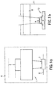
- Lens system 1 is used in a digital camera 6, as shown in figure 1, in which the lens system 1 is secured within a housing (not shown) to project an image on an image sensor 7 positioned at the image plane 5 of the camera 6.
- the assembly of lens is adjusted, as shown in figure 4a - 4c to obtain autofocus and zoom functions.
- the mechanical movement of the lens system 1 is constructed using advanced micro-machining techniques.
- a semi-conductor image sensor can be combined with a lens system in a unique manner to obtain substantially the same functions as described above.
- the resulting image generating system can be exceedingly small and therefore can be conveniently packaged within the confines of a mobile communications device, such as a cellular telephone.
- a semi-conductor image sensor 9 is supported for movement by a micro-machined actuator assembly 10 in operative association with lens system 8 and positioned within the housing 11 of a digital camera or mobile communication device.
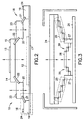
- the actuating assembly 10 of the digital camera is shown in more detail in figure 2.
- an image sensor 13 is constructed with its associated electronics on a semi-conductor chip 14.
- Terminal 15 provides the sensor 13 with appropriate electrical contact to power the sensor 13.
- a micro-electrical mechanical system (MEMS) 16 is formed on substrate 17 to support the sensor 13.
- MEMS 16 may take many different forms depending on the function of the camera and the fabricating technique used.
- a series of electrostatic resonators 18 are schematically shown.
- Electrostatic resonator 18 is an example of a linear actuator that can be used as a precise positioner, among other things.
- Actuator 18 consists of a pair of bases 19 which are fixed to the substrate 17 and moveable supports 20.
- Supports 20 are connected to bases 19 by means of electrostatic fingers 21.
- Sensor chip 13 is connected to movable supports 20 by a further pair of electrostatic fingers 22.
- the moveable supports 20 and the sensor chip 13 can be moved by applying a voltage between the moveable structure and its immediately adjacent supporting structure.
- contacts 23 are provided on moveable support 20 and contacts 24 are provided on bases 19.
- the actuating assembly 10 as shown in figure 2, provides a two position motion utilizing the movement of moveable supports 20 on their associated bases 19 and the movement of the sensor 13 on supports 20.
- the sensor 13 is shown mounted on the substrate 17, this particular embodiment could be adapted to provide autofocus, if used within a conventional lens system. If however the sensor 13 was mounted on the substrate 17 (see phantom lines 12) and replaced by a lens mounted on the illustrated support assembly, a zoom mechanism could be provided.
- a MEMS support assembly which may be adapted to provide both autofocus and zoom functions.
- a lens 24 is mounted on a three position (or smoothly variable) MEMS support assembly 25 to the substrate 26 through base element 27.
- An image sensor 28 is also mounted for independent motion on a two position MEMS support 29. This system may be adapted to provide both an autofocus and a zoom capability.
- the image sensor used herein is a semiconductor C-MOS sensor array constructed using standard silicon processing techniques which are compatible with the MEMS fabrication process.
- appropriate electronic or manual systems would be connected to initiate operation of the functions provided.
- the sensor array is constructed on a chip with imbedded control circuitry including sensors, memory, and other functions.
- the MEMS technique used may be surface micro-machining. This method is an additive fabrication technique which involves the building of the device on top of the supporting substrate.
- the substrate would be constructed with the necessary imbedded control circuitry, for example as an application specific semi-conductor integrated circuit.
- the digital image sensor and the micro-electromechanical zoom are manufactured on the same chip using silicon based microelectronics for the sensor and micromachining technology for the micro-electromechanical support.
- a micro-miniature digital camera having a variety of basic functions can be fabricated in a cost effective manner for use with a mobile communication device.
Landscapes
- Engineering & Computer Science (AREA)
- Multimedia (AREA)
- Signal Processing (AREA)
- Physics & Mathematics (AREA)
- General Engineering & Computer Science (AREA)
- General Physics & Mathematics (AREA)
- Optics & Photonics (AREA)
- Lens Barrels (AREA)
- Studio Devices (AREA)
Abstract
Description
- This invention relates to a camera configuration and has particular but not exclusive application to a camera incorporated in a mobile communications device
- Mobile communications devices are becoming more compact while their functions and features are ever expanding. As a next step in this process of expanding applications, a digital camera may be installed. This requires a new cycle of development with respect to the digital camera in order to package the necessary functions within the compact profile of the mobile communications device. In order to miniaturize the camera for such use, the zoom feature is often eliminated or substantially reduced in functionality. This is because the apparatus needed to move the lens in a traditional zoom mechanism is cumbersome. The development is facilitated by the introduction of digital, semi-conductor, imaging sensors, such as CCD and C-MOS sensor arrays.
- In addition a new class of micro-miniature components have become available that provide the functionality of both electrical and mechanical components. These components are fabricated in a process similar to the manufacture of integrated circuit chips, namely the surface treatment of silicon wafers. These mechanisms can provide the function of sensors (resonators), actuators, transducers, motors, and gears to high tolerances. By micro-machining silicon wafers layered on a substrate, the components, of the so called micro-electomechanical system (MEMS), are constructed on a thin substrate. A description of MEMS components is contained in Philosophical Transactions of the Royal Society: Physical Sciences and Engineering, Series A, Issue no. 1703, December 15, 1995, pp. 355-366, which is incorporated herein by reference.
- It is a purpose of this invention to provide an autofocus and zoom system for a compact electronic device. A further purpose of this invention is to provide these functions by using a sensor array, such as a C-MOS sensor array, and a lens actuation mechanism suitable for fabrication on a silicon wafer. It is a further purpose of this invention to utilize the advantages of micro-electromechanical system (MEMS) manufacturing techniques to obtain these goals.
- In accordance with the invention there is provided a miniaturized digital camera that may be constructed for use with a mobile communication device or other compact appliance. The optical system of the camera may consist of a small lens system having the traditional components of a primary lens, a variator lens, and a compensator lens. The lens system transmits the image received from an external source to a sensor array. The sensor array may be constructed on a substrate using silicon wafer fabrication techniques and is positioned to receive the image from the lens system. The array may be operatively associated with a micro-electro mechanical component for movement between at least two positions by actuation of the MEMS component. Both the array and the MEMS component are constructed on the same substrate utilizing similar techniques to create an extremely small fully functional imaging system for use with the lens system. Actuation of the MEMS component, will move the sensor array relative to the lens system. Such actuation of the MEMS component, can be accomplished in response to, for example, the sensed distance of the lens system from the subject of the image. In this manner an autofocus function can be accomplished. The movement of the sensor is combined with a coordinated movement of the variator and/or compensator lenses to provide a zoom function. To facilitate this coordinated movement one or both of these lens can be mounted for movement on the MEMS component in operative association with the sensor array. Since the position of the sensor array can be varied the movement of the lens-system/lenses could in some cases be reduced. With a suitable lens design and by moving the sensor array itself, it could e.g. be possible to reduce or completely omit the movement of one of the lenses, e.g. the compensator. In this manner a variety of configurations can be accomplished to provide the zoom and autofocus functions in a miniaturized version of the traditional system.
- The subject invention is described in more detail below by way of example with reference to the drawing in which:
- Figure 1a is a schematic illustration of a traditional lens system with a fixed sensor array;
- Figure 1b is a schematic illustration of a lens system in which the sensor array is mounted for movement;
- Figure 2 is a schematic illustration of the sensor array of this invention fabricated with the MEMS component for multiple positions;
- Figure 3 is a schematic illustration of the sensor array and lens system fabricated and mounted for coordinated movement on the MEMS component; and
- Figures 4a, 4b, and 4c are schematic illustrations of a traditional lens system, showing the various relative positions of the lenses.
-
- A typical
optical lens system 1 for a camera having autofocus and zoom capability is depicted schematically in Figures 4a - 4c. It generally consists of aprimary lens 2, avariator lens 3, and acompensator lens 4 which are operatively associated to project a focused image onimage plane 5. As shown, the lens has three "principal" positions, i.e., wide angle, middle and telephoto. The zoom function can be a smooth movement between the two end positions (wide and tele) and do not necessarily have to be a stepwise action with only three options. These variations in function are provided by moving the variator and compensator lens, 3 and 4 respectively, as shown.Lens system 1 is used in adigital camera 6, as shown in figure 1, in which thelens system 1 is secured within a housing (not shown) to project an image on animage sensor 7 positioned at theimage plane 5 of thecamera 6. The assembly of lens is adjusted, as shown in figure 4a - 4c to obtain autofocus and zoom functions. - In accordance with this invention, the mechanical movement of the
lens system 1 is constructed using advanced micro-machining techniques. Through such techniques, a semi-conductor image sensor can be combined with a lens system in a unique manner to obtain substantially the same functions as described above. The resulting image generating system can be exceedingly small and therefore can be conveniently packaged within the confines of a mobile communications device, such as a cellular telephone. As shown in figure 1b, asemi-conductor image sensor 9 is supported for movement by amicro-machined actuator assembly 10 in operative association withlens system 8 and positioned within thehousing 11 of a digital camera or mobile communication device. - The actuating
assembly 10 of the digital camera is shown in more detail in figure 2. In theactuating assembly 10, animage sensor 13 is constructed with its associated electronics on asemi-conductor chip 14.Terminal 15 provides thesensor 13 with appropriate electrical contact to power thesensor 13. A micro-electrical mechanical system (MEMS) 16 is formed onsubstrate 17 to support thesensor 13. MEMS 16 may take many different forms depending on the function of the camera and the fabricating technique used. For the purpose of illustration, a series ofelectrostatic resonators 18 are schematically shown.Electrostatic resonator 18 is an example of a linear actuator that can be used as a precise positioner, among other things.Actuator 18 consists of a pair ofbases 19 which are fixed to thesubstrate 17 andmoveable supports 20.Supports 20 are connected tobases 19 by means ofelectrostatic fingers 21.Sensor chip 13 is connected tomovable supports 20 by a further pair ofelectrostatic fingers 22. The moveable supports 20 and thesensor chip 13 can be moved by applying a voltage between the moveable structure and its immediately adjacent supporting structure. For thispurpose contacts 23 are provided onmoveable support 20 andcontacts 24 are provided onbases 19. Theactuating assembly 10, as shown in figure 2, provides a two position motion utilizing the movement ofmoveable supports 20 on their associatedbases 19 and the movement of thesensor 13 onsupports 20. For further information, see the article entitled "What is MEMS" at http//www.mems.engr.wisc.edu. - Since, as shown in figure 2, the
sensor 13 is shown mounted on thesubstrate 17, this particular embodiment could be adapted to provide autofocus, if used within a conventional lens system. If however thesensor 13 was mounted on the substrate 17 (see phantom lines 12) and replaced by a lens mounted on the illustrated support assembly, a zoom mechanism could be provided. - In the alternate embodiment shown in figure 3, a MEMS support assembly is shown which may be adapted to provide both autofocus and zoom functions. In this embodiment, a
lens 24 is mounted on a three position (or smoothly variable)MEMS support assembly 25 to thesubstrate 26 throughbase element 27. Animage sensor 28 is also mounted for independent motion on a twoposition MEMS support 29. This system may be adapted to provide both an autofocus and a zoom capability. - The image sensor used herein is a semiconductor C-MOS sensor array constructed using standard silicon processing techniques which are compatible with the MEMS fabrication process. In addition, appropriate electronic or manual systems would be connected to initiate operation of the functions provided. Ideally, the sensor array is constructed on a chip with imbedded control circuitry including sensors, memory, and other functions.
- The MEMS technique used may be surface micro-machining. This method is an additive fabrication technique which involves the building of the device on top of the supporting substrate. The substrate would be constructed with the necessary imbedded control circuitry, for example as an application specific semi-conductor integrated circuit. In this way the digital image sensor and the micro-electromechanical zoom are manufactured on the same chip using silicon based microelectronics for the sensor and micromachining technology for the micro-electromechanical support.
- In this manner, a micro-miniature digital camera having a variety of basic functions can be fabricated in a cost effective manner for use with a mobile communication device.
Claims (8)
- A camera system comprising:a lens assembly mounted for receiving an image and projecting said image on an image plane;a micro-electromechanical system (MEMS) support mechanism for providing at least two positions of movement to a supported element, said MEMS support mechanism being fabricated integrally with said supported element; anda semi-conductor image sensor mounted at said image plane for movement on said MEMS support mechanism and being operatively associated with said lens to generate a electrical signals corresponding to said image.
- A camera system, according to claim 1, wherein said MEMS is an electrostatic resonator.
- A camera system, according to claim 1 or 2, wherein the image sensor is fabricated on a silicon chip in which is imbedded control circuitry and said MEMS is integrally fabricated therewith.
- A camera system according to claim 1, 2 or 3 wherein said movement of said image sensor provides an auto focus function.
- A camera system, according to claim 1, wherein said lens assembly is mounted for movement on said MEMS for movement relative to said image sensor and said image sensor is fixed, said movement adapted to provide a zoom function.
- A camera system according to claim 1, further comprising:a substrate for supporting said digital camera system;a first MEMS fabricated on said substrate and connected to said lens system for providing movement of said lens system between at least two positions;a second MEMS fabricated on said substrate and connected to said image sensor for providing movement of said image sensor between at least two positions; andwherein said movement of said lens system and said image sensor is relative to each other to provide both an autofocus and zoom function.
- A camera system according to any preceding claim wherein the image sensor is operable to produce digital signals corresponding to the image.
- A mobile communication device including a housing containing a system to transmit data over a communication network, said housing containing a camera system according to any preceding claim.
Applications Claiming Priority (2)
| Application Number | Priority Date | Filing Date | Title |
|---|---|---|---|
| US09/779,416 US6914635B2 (en) | 2001-02-08 | 2001-02-08 | Microminiature zoom system for digital camera |
| US779416 | 2001-02-08 |
Publications (1)
| Publication Number | Publication Date |
|---|---|
| EP1231781A1 true EP1231781A1 (en) | 2002-08-14 |
Family
ID=25116373
Family Applications (1)
| Application Number | Title | Priority Date | Filing Date |
|---|---|---|---|
| EP02250616A Withdrawn EP1231781A1 (en) | 2001-02-08 | 2002-01-29 | Camera configuration |
Country Status (2)
| Country | Link |
|---|---|
| US (1) | US6914635B2 (en) |
| EP (1) | EP1231781A1 (en) |
Families Citing this family (58)
| Publication number | Priority date | Publication date | Assignee | Title |
|---|---|---|---|---|
| US7813634B2 (en) * | 2005-02-28 | 2010-10-12 | Tessera MEMS Technologies, Inc. | Autofocus camera |
| US6850675B1 (en) | 2002-02-04 | 2005-02-01 | Siwave, Inc. | Base, payload and connecting structure and methods of making the same |
| US7663289B1 (en) | 2004-02-18 | 2010-02-16 | Siimpel Corporation | Centipede actuator motion stage |
| US7477842B2 (en) * | 2004-03-12 | 2009-01-13 | Siimpel, Inc. | Miniature camera |
| US7640803B1 (en) | 2004-05-26 | 2010-01-05 | Siimpel Corporation | Micro-electromechanical system inertial sensor |
| FR2881847A1 (en) * | 2005-02-10 | 2006-08-11 | St Microelectronics Sa | Optical device for e.g. mobile telephone, has auto focus camera module with optical chip having microprocessor to process, based on image signals from image sensor, control signal applied to focussing units to ensure auto focus of objective |
| US20060192885A1 (en) * | 2005-02-28 | 2006-08-31 | Siimpel | Miniature camera bias spring |
| TWI484245B (en) * | 2005-02-28 | 2015-05-11 | Digitaloptics Corp Mems | Autofocus camera |
| US7729603B2 (en) * | 2005-02-28 | 2010-06-01 | Siimpel Corporation | Resolution adjustment for miniature camera |
| US7838322B1 (en) | 2005-02-28 | 2010-11-23 | Tessera MEMS Technologies, Inc. | Method of enhancing an etch system |
| US20060192858A1 (en) * | 2005-02-28 | 2006-08-31 | Calvet Robert J | Oil damping for camera optical assembly |
| US7555210B2 (en) * | 2005-02-28 | 2009-06-30 | Siimpel, Inc. | Axial snubbers for camera |
| JP4123250B2 (en) * | 2005-06-24 | 2008-07-23 | 松下電器産業株式会社 | Image sensor driving apparatus and imaging apparatus using the same |
| US7583006B2 (en) * | 2005-07-26 | 2009-09-01 | Siimpel Corporation | MEMS digital linear actuator |
| US20070041723A1 (en) * | 2005-08-22 | 2007-02-22 | Gutierrez Roman C | Elongated camera system for cellular telephones |
| US7477400B2 (en) * | 2005-09-02 | 2009-01-13 | Siimpel Corporation | Range and speed finder |
| CN1928612B (en) * | 2005-09-09 | 2010-05-05 | 鸿富锦精密工业(深圳)有限公司 | Digital camera zoom structure |
| US20070065131A1 (en) * | 2005-09-20 | 2007-03-22 | Chengping Wei | Auto-focusing and Zooming Systems and Method of Operating Same |
| ATE467147T1 (en) * | 2006-05-24 | 2010-05-15 | Stueckler Gerd | METHOD FOR SPACE FILTERING AND IMAGE RECORDING DEVICE |
| US8619378B2 (en) | 2010-11-15 | 2013-12-31 | DigitalOptics Corporation MEMS | Rotational comb drive Z-stage |
| US8768157B2 (en) | 2011-09-28 | 2014-07-01 | DigitalOptics Corporation MEMS | Multiple degree of freedom actuator |
| WO2008133943A1 (en) | 2007-04-24 | 2008-11-06 | Flextronics Ap Llc | Small form factor modules using wafer level optics with bottom cavity and flip chip assembly |
| US7825985B2 (en) * | 2007-07-19 | 2010-11-02 | Flextronics Ap, Llc | Camera module back-focal length adjustment method and ultra compact components packaging |
| CN101408655B (en) * | 2007-10-11 | 2011-07-27 | 鸿富锦精密工业(深圳)有限公司 | Lens module |
| CN101420526B (en) * | 2007-10-26 | 2011-06-08 | 鸿富锦精密工业(深圳)有限公司 | Image sensor bearing device and camera module group |
| US7615729B2 (en) * | 2007-12-10 | 2009-11-10 | Aptina Imaging Corporation | Apparatus and method for resonant lens focusing |
| US7920343B2 (en) * | 2009-01-14 | 2011-04-05 | Aptina Imaging Corporation | Method of forming lens arrays and transferring such onto movable-MEMS structures |
| JP5839786B2 (en) * | 2010-07-12 | 2016-01-06 | キヤノン株式会社 | Image pickup apparatus and tracking data adjustment method |
| US8605375B2 (en) | 2010-11-15 | 2013-12-10 | DigitalOptics Corporation MEMS | Mounting flexure contacts |
| US8337103B2 (en) | 2010-11-15 | 2012-12-25 | DigitalOptics Corporation MEMS | Long hinge actuator snubbing |
| US8547627B2 (en) | 2010-11-15 | 2013-10-01 | DigitalOptics Corporation MEMS | Electrical routing |
| US9019390B2 (en) | 2011-09-28 | 2015-04-28 | DigitalOptics Corporation MEMS | Optical image stabilization using tangentially actuated MEMS devices |
| US8521017B2 (en) | 2010-11-15 | 2013-08-27 | DigitalOptics Corporation MEMS | MEMS actuator alignment |
| US9061883B2 (en) | 2010-11-15 | 2015-06-23 | DigitalOptics Corporation MEMS | Actuator motion control features |
| US8637961B2 (en) | 2010-11-15 | 2014-01-28 | DigitalOptics Corporation MEMS | MEMS actuator device |
| US8941192B2 (en) | 2010-11-15 | 2015-01-27 | DigitalOptics Corporation MEMS | MEMS actuator device deployment |
| US8604663B2 (en) | 2010-11-15 | 2013-12-10 | DigitalOptics Corporation MEMS | Motion controlled actuator |
| US8608393B2 (en) | 2010-11-15 | 2013-12-17 | DigitalOptics Corporation MEMS | Capillary actuator deployment |
| US8947797B2 (en) | 2010-11-15 | 2015-02-03 | DigitalOptics Corporation MEMS | Miniature MEMS actuator assemblies |
| US8884381B2 (en) | 2010-11-15 | 2014-11-11 | DigitalOptics Corporation MEMS | Guard trench |
| US9515579B2 (en) | 2010-11-15 | 2016-12-06 | Digitaloptics Corporation | MEMS electrical contact systems and methods |
| US9052567B2 (en) | 2010-11-15 | 2015-06-09 | DigitalOptics Corporation MEMS | Actuator inside of motion control |
| US8358925B2 (en) | 2010-11-15 | 2013-01-22 | DigitalOptics Corporation MEMS | Lens barrel with MEMS actuators |
| US9352962B2 (en) | 2010-11-15 | 2016-05-31 | DigitalOptics Corporation MEMS | MEMS isolation structures |
| US8803256B2 (en) | 2010-11-15 | 2014-08-12 | DigitalOptics Corporation MEMS | Linearly deployed actuators |
| US8430580B2 (en) | 2010-11-15 | 2013-04-30 | DigitalOptics Corporation MEMS | Rotationally deployed actuators |
| US10009528B2 (en) | 2011-02-24 | 2018-06-26 | Nan Chang O-Film Optoelectronics Technology Ltd | Autofocus camera module packaging with circuitry-integrated actuator system |
| US8545114B2 (en) | 2011-03-11 | 2013-10-01 | Digitaloptics Corporation | Auto focus-zoom actuator or camera module contamination reduction feature with integrated protective membrane |
| US8724201B2 (en) | 2011-07-20 | 2014-05-13 | Brian Albus | MEMS actuator and MEMS actuated shutter mechanism |
| US8853975B2 (en) | 2011-09-28 | 2014-10-07 | DigitalOptics Corporation MEMS | Electrostatic actuator control |
| US8869625B2 (en) | 2011-09-28 | 2014-10-28 | DigitalOptics Corporation MEMS | MEMS actuator/sensor |
| US8571405B2 (en) | 2011-09-28 | 2013-10-29 | DigitalOptics Corporation MEMS | Surface mount actuator |
| US8855476B2 (en) | 2011-09-28 | 2014-10-07 | DigitalOptics Corporation MEMS | MEMS-based optical image stabilization |
| US9350271B2 (en) | 2011-09-28 | 2016-05-24 | DigitalOptics Corporation MEMS | Cascaded electrostatic actuator |
| US8616791B2 (en) | 2011-09-28 | 2013-12-31 | DigitalOptics Corporation MEMS | Rotationally deployed actuator devices |
| US9281763B2 (en) | 2011-09-28 | 2016-03-08 | DigitalOptics Corporation MEMS | Row and column actuator control |
| US8711495B2 (en) | 2012-10-01 | 2014-04-29 | Apple Inc. | MEMS autofocus actuator |
| CN103837980B (en) * | 2012-11-22 | 2015-11-25 | 上海丽恒光微电子科技有限公司 | Based on the aperture adjusting device and preparation method thereof of MEMS |
-
2001
- 2001-02-08 US US09/779,416 patent/US6914635B2/en not_active Expired - Lifetime
-
2002
- 2002-01-29 EP EP02250616A patent/EP1231781A1/en not_active Withdrawn
Non-Patent Citations (4)
| Title |
|---|
| KOGA A ET AL: "Electrostatic linear microactuator mechanism for focusing a CCD camera", JOURNAL OF LIGHTWAVE TECHNOLOGY, JAN. 1999, IEEE, USA, vol. 17, no. 1, pages 43 - 47, XP002199041, ISSN: 0733-8724 * |
| MOTAMEDI M E: "MICRO-OPTO-ELECTRO-MECHANICAL SYSTEMS", OPTICAL ENGINEERING, SOC. OF PHOTO-OPTICAL INSTRUMENTATION ENGINEERS. BELLINGHAM, US, vol. 33, no. 11, 1 November 1994 (1994-11-01), pages 3505 - 3517, XP000475094, ISSN: 0091-3286 * |
| RUSSELL E: "CREATING THE RIGHT IMAGE CMOS TECHNOLOGY IS SET TO DISPLACE THE CHARGE COUPLED DEVICE", NEW ELECTRONICS, INTERNATIONAL THOMSON PUBLISHING, LONDON, GB, vol. 33, no. 16, 26 September 2000 (2000-09-26), pages 23 - 24, XP000959346, ISSN: 0047-9624 * |
| SCHEITER T ET AL: "PURE CMOS MICROSYSTEMS - THE SIEMENS APPROACH FOR LOW COST MICROSYSTEMS IN HIGH VOLUME MARKETS", MICROSYSTEM SYMPOSIUM PROCEEDINGS, XX, XX, 10 September 1998 (1998-09-10), pages 77 - 85, XP000865534 * |
Also Published As
| Publication number | Publication date |
|---|---|
| US6914635B2 (en) | 2005-07-05 |
| US20040201773A1 (en) | 2004-10-14 |
Similar Documents
| Publication | Publication Date | Title |
|---|---|---|
| US6914635B2 (en) | Microminiature zoom system for digital camera | |
| US10520747B2 (en) | Lens module | |
| US6710950B2 (en) | Piezoelectric actuator for digital camera optical system | |
| US6747784B2 (en) | Compliant mechanism and method of forming same | |
| KR101245059B1 (en) | Camera module and portable terminal employing the same | |
| CN107942600B (en) | Camera module | |
| KR100864691B1 (en) | Varifocal mirror and camera module using the same | |
| CN212723526U (en) | MEMS actuators | |
| KR20160081243A (en) | Camera Module | |
| US20100084726A1 (en) | Wafer level packaging image sensor module having lens actuator and method of manfacturing the same | |
| CN110955010A (en) | Liquid lens focusing and stabilization mechanisms, camera modules and electronics | |
| KR102019098B1 (en) | Micro electro mechanical systems device | |
| KR100951910B1 (en) | Focusing Device and Imaging Device | |
| KR100657002B1 (en) | Electromagnetic drive variable focus mirror, manufacturing method and driving method thereof | |
| US20240272519A1 (en) | Actuator for camera | |
| WO2008117958A1 (en) | Auto focus camera module | |
| US20240345360A1 (en) | Hybrid actuator for zoom driving | |
| US8000590B2 (en) | Driving apparatus, image capturing unit, and image capturing apparatus | |
| KR20100134407A (en) | Camera Module Using Piezo Actuator | |
| KR20080076364A (en) | Compact optical lens drive | |
| KR102516773B1 (en) | Sensor Actuator and Camera Module Including Same | |
| JP2006098595A (en) | Camera module and portable terminal equipped with the camera module | |
| KR20180052591A (en) | Camera module | |
| KR102204647B1 (en) | Micro electro mechanical systems device and camera module having the same | |
| US12585168B2 (en) | Zooming actuator having dual structure |
Legal Events
| Date | Code | Title | Description |
|---|---|---|---|
| PUAI | Public reference made under article 153(3) epc to a published international application that has entered the european phase |
Free format text: ORIGINAL CODE: 0009012 |
|
| AK | Designated contracting states |
Kind code of ref document: A1 Designated state(s): AT BE CH CY DE DK ES FI FR GB GR IE IT LI LU MC NL PT SE TR |
|
| AX | Request for extension of the european patent |
Free format text: AL;LT;LV;MK;RO;SI |
|
| 17P | Request for examination filed |
Effective date: 20030130 |
|
| AKX | Designation fees paid |
Designated state(s): AT BE CH CY DE DK ES FI FR GB GR IE IT LI LU MC NL PT SE TR |
|
| 17Q | First examination report despatched |
Effective date: 20061128 |
|
| GRAP | Despatch of communication of intention to grant a patent |
Free format text: ORIGINAL CODE: EPIDOSNIGR1 |
|
| STAA | Information on the status of an ep patent application or granted ep patent |
Free format text: STATUS: THE APPLICATION IS DEEMED TO BE WITHDRAWN |
|
| 18D | Application deemed to be withdrawn |
Effective date: 20070801 |