EP1231499A2 - Elément optique pour dispositif d'affichage par projection - Google Patents
Elément optique pour dispositif d'affichage par projection Download PDFInfo
- Publication number
- EP1231499A2 EP1231499A2 EP02010139A EP02010139A EP1231499A2 EP 1231499 A2 EP1231499 A2 EP 1231499A2 EP 02010139 A EP02010139 A EP 02010139A EP 02010139 A EP02010139 A EP 02010139A EP 1231499 A2 EP1231499 A2 EP 1231499A2
- Authority
- EP
- European Patent Office
- Prior art keywords
- light
- polarization
- film
- transparent members
- optical element
- Prior art date
- Legal status (The legal status is an assumption and is not a legal conclusion. Google has not performed a legal analysis and makes no representation as to the accuracy of the status listed.)
- Withdrawn
Links
Images


Classifications
-
- G—PHYSICS
- G02—OPTICS
- G02F—OPTICAL DEVICES OR ARRANGEMENTS FOR THE CONTROL OF LIGHT BY MODIFICATION OF THE OPTICAL PROPERTIES OF THE MEDIA OF THE ELEMENTS INVOLVED THEREIN; NON-LINEAR OPTICS; FREQUENCY-CHANGING OF LIGHT; OPTICAL LOGIC ELEMENTS; OPTICAL ANALOGUE/DIGITAL CONVERTERS
- G02F1/00—Devices or arrangements for the control of the intensity, colour, phase, polarisation or direction of light arriving from an independent light source, e.g. switching, gating or modulating; Non-linear optics
- G02F1/01—Devices or arrangements for the control of the intensity, colour, phase, polarisation or direction of light arriving from an independent light source, e.g. switching, gating or modulating; Non-linear optics for the control of the intensity, phase, polarisation or colour
- G02F1/015—Devices or arrangements for the control of the intensity, colour, phase, polarisation or direction of light arriving from an independent light source, e.g. switching, gating or modulating; Non-linear optics for the control of the intensity, phase, polarisation or colour based on semiconductor elements with at least one potential jump barrier, e.g. PN, PIN junction
-
- H—ELECTRICITY
- H04—ELECTRIC COMMUNICATION TECHNIQUE
- H04N—PICTORIAL COMMUNICATION, e.g. TELEVISION
- H04N9/00—Details of colour television systems
- H04N9/12—Picture reproducers
- H04N9/31—Projection devices for colour picture display, e.g. using electronic spatial light modulators [ESLM]
- H04N9/3102—Projection devices for colour picture display, e.g. using electronic spatial light modulators [ESLM] using two-dimensional electronic spatial light modulators
- H04N9/3105—Projection devices for colour picture display, e.g. using electronic spatial light modulators [ESLM] using two-dimensional electronic spatial light modulators for displaying all colours simultaneously, e.g. by using two or more electronic spatial light modulators
-
- G—PHYSICS
- G02—OPTICS
- G02B—OPTICAL ELEMENTS, SYSTEMS OR APPARATUS
- G02B27/00—Optical systems or apparatus not provided for by any of the groups G02B1/00 - G02B26/00, G02B30/00
- G02B27/28—Optical systems or apparatus not provided for by any of the groups G02B1/00 - G02B26/00, G02B30/00 for polarising
- G02B27/283—Optical systems or apparatus not provided for by any of the groups G02B1/00 - G02B26/00, G02B30/00 for polarising used for beam splitting or combining
- G02B27/285—Optical systems or apparatus not provided for by any of the groups G02B1/00 - G02B26/00, G02B30/00 for polarising used for beam splitting or combining comprising arrays of elements, e.g. microprisms
-
- H—ELECTRICITY
- H04—ELECTRIC COMMUNICATION TECHNIQUE
- H04N—PICTORIAL COMMUNICATION, e.g. TELEVISION
- H04N9/00—Details of colour television systems
- H04N9/12—Picture reproducers
- H04N9/31—Projection devices for colour picture display, e.g. using electronic spatial light modulators [ESLM]
- H04N9/3141—Constructional details thereof
- H04N9/315—Modulator illumination systems
- H04N9/3167—Modulator illumination systems for polarizing the light beam
-
- H—ELECTRICITY
- H04—ELECTRIC COMMUNICATION TECHNIQUE
- H04N—PICTORIAL COMMUNICATION, e.g. TELEVISION
- H04N5/00—Details of television systems
- H04N5/74—Projection arrangements for image reproduction, e.g. using eidophor
- H04N5/7416—Projection arrangements for image reproduction, e.g. using eidophor involving the use of a spatial light modulator, e.g. a light valve, controlled by a video signal
- H04N5/7441—Projection arrangements for image reproduction, e.g. using eidophor involving the use of a spatial light modulator, e.g. a light valve, controlled by a video signal the modulator being an array of liquid crystal cells
Definitions
- the present invention relates to an optical element suitable for a projection display apparatus, and a method for fabricating the optical element.
- Japanese Patent Laid-open Gazette No. 7-294906 discloses an optical element, called polarization converting element, for use in converting light having random polarization directions to light having one polarization direction.
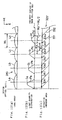
- Such an optical element is shown in plan view in Fig. 1(A) and in perspective view in Fig. 1(B).
- This optical element comprises a polarization beam splitter array 22 comprising alternately adhered linear polarization beam splitters 30 having polarization splitting films 36 and linear prisms 40 having reflecting films 46. Portions of the exit surface of the polarization beam splitter array 22 are selectively provided with ⁇ /2 optical phase plates 24.
- the linear polarization beam splitter 30 includes two rectangular prisms 32, 34 and the polarization splitting film 36 formed at the slant plane constituted by the interface between the rectangular prisms 32, 34.
- the polarization splitting film 36 is formed on the slant plane of one of the rectangular prisms and the two rectangular prisms 32, 34 are then bonded with an optical adhesive.
- the linear prism 40 includes two rectangular prisms 42, 44 and the reflecting film 46 formed at the slant plane at the interface between rectangular prisms 42, 44.
- the reflecting film 46 is formed on the slant plane of one of the rectangular prisms, and the two rectangular prisms 42, 44 are then bonded with an optical adhesive.
- the reflecting film 46 is formed of an aluminum or other metal film.
- linear polarization beam splitters 30 and linear prisms 40 prepared in this manner are adhered alternately with an optical adhesive to fabricate the polarization beam splitter array 22.
- the ⁇ /2 optical phase plates 24 are then selectively bonded to the exit surface of the linear polarization beam splitter 30.
- Light including an S polarized light component and a P polarized light component enters from the incident surface.
- the incident light is first separated into S polarized light and P polarized light by the polarization splitting film 36.
- the S polarized light is reflected at substantially a right angle by the polarization splitting film 36, is further reflected at a right angle by the reflecting film 46, and exits the prism 40.
- the P polarized light passes straight through the polarization splitting film 36, is converted to S polarized light by the ⁇ /2 optical phase plate 24, and exits therefrom.
- a light beam having random polarization directions entering this optical element emerges entirely as an S polarized light beam.
- the conventional optical element shown in Figs. 1(A) and 1(B) has four rectangular prisms 32, 34, 42, 44 adhered by optical adhesive. Between entering and exiting the optical element, the S polarized light and P polarized light must therefore pass repeatedly through the optical adhesive layers formed at the prism interfaces. Since the optical adhesive absorbs some of the light, the intensity of the light decreases with each passage through an optical adhesive layer. This results in a considerable decline in light utilization efficiency.
- an object of the present invention at least in the preferred embodiments is to enhance the light utilization efficiency of the optical element. Another object is to provide an optical element which is easy to fabricate.
- the present invention provides an optical element comprising a plurality of first transparent members and a plurality of second transparent members, which are alternately arranged with and secured to each other.
- Each of the plurality of first transparent members has a first incident surface and a first exit surface substantially parallel to each other, first and second film forming surfaces substantially parallel to each other and making a prescribed angle with the first incident surface and the first exit surface.
- a polarization splitting film is formed on the first film forming surface, and a reflecting film is formed on the second film forming surface.
- Each of the plurality of second transparent members has a second incident surface and a second exit surface parallel to each other.
- the plurality of second transparent members are alternately arranged with and secured to the plurality of first transparent members at the first and second film forming surfaces across the polarization splitting film and the reflecting film respectively so that the second incident surfaces are aligned with the first incident surfaces to form an incident plane and that the second exit surfaces are aligned with the first exit surfaces to form an exit plane.
- the polarized light component thereof reflected by the polarizing-splitting film is reflected by the reflecting film without passing through a layer of optical adhesive and then exits from the optical element.
- the light utilization efficiency is improved because the number of times this polarized light component passes through layers of the optical adhesive can therefore be reduced.
- the reflecting film has a dielectric multi-layer film.
- a reflecting film formed of a multi-layer dielectric films enables the reflectance for a specific linearly polarized light component to be increased over that in the case of a reflecting film formed of an aluminum or other metal film. A further increase in the light utilization efficiency can therefore be attained.
- the optical element further comprises polarization direction converting means associated with either of the first exit surface and the second exit surface.
- Linearly polarized light components of different polarization direction exit from the exit surface portion of the first transparent member and the exit surface portion of the second transparent member.
- the optical element may further comprise light shielding means associated with the second incident surface. If light enters from the second incident surface of the second transparent member, this light will, after reflection by the reflecting film, pass through optical adhesive layers repeatedly before being converted into S polarized light and P polarized light by the polarization splitting film. If this kind of light is shut out by providing light shielding means with respect to the second incident surface of the second transparent member, repeated passage of the light entering the optical element through optical adhesive layers can be prevented.
- the optical element further comprises adhesive layers between the first and second transparent members, and at least one of a thickness of the adhesive layers and thicknesses of the first and second transparent members are adjusted to make intervals between the polarization splitting films and the reflecting films substantially constant throughout the optical element. Since this makes the intervals between the polarization splitting films and the reflecting films equal, the positional accuracy of the films in the optical element can be improved to increase the light utilization efficiency.
- the thickness of the second transparent members is set smaller than the thickness of the first transparent member. More preferably, the thickness of the second transparent member is in the range of 80% to 90% of the thickness of the first transparent member. For example, the thickness of the first transparent members is equal to a value obtained by adding twice the thickness of the adhesive layers to the thickness of the second transparent members.
- the optical element may be used with a plurality of small lenses which will be arranged on the incident plane, and the intervals between the plurality of polarization splitting films may substantially correspond to a pitch of the plurality of small lenses. This makes the intervals between the polarization splitting films and the reflecting films constant, thereby increasing the light utilization efficiency of the optical element.
- At least one of a thickness of the adhesive layers and thicknesses of the first and second transparent members are adjusted to make the intervals between the plurality of polarization splitting films substantially correspond to a pitch of an optical axes of the plurality of small lenses. Since this provides a configuration enabling each of multiple light beams exiting from multiple small lenses to fall incident on a polarization splitting film associated therewith, it improves the light utilization efficiency.
- the plurality of small lenses have a plurality of different optical axis pitches, and at least one of the thickness of the adhesive layers and the thicknesses of the first and second transparent members are adjusted to make the intervals between the plurality of polarization splitting films substantially correspond to the plurality of different optical axis pitches.
- the optical element can be used with a plurality of small lenses which will be arranged on the incident plane.
- intervals between the plurality of polarization splitting films may substantially correspond to a pitch of a plurality of light beams exiting from the plurality of small lenses.
- the pitch of the light beams exiting from the small lenses does not always coincide with the pitch of the lens optical axes. This configuration enables each light beam exiting from the small lenses to fall incident on the associated polarization splitting film even in such a case. It thus improves the light utilization efficiency.
- At least one of the thickness of the adhesive layers and the thicknesses of the first and second transparent members may be adjusted to make the intervals between the plurality of polarization splitting films substantially correspond to the pitch of the plurality of light beams exiting from the plurality of small lenses.
- a method for fabricating an optical element comprises the steps of: (a) providing a plurality of first transparent members each having substantially parallel first and second surfaces, and a plurality of second transparent members each having two substantially parallel surfaces; (b) forming a polarization splitting film on the first surface of each the first transparent member; (c) forming a reflecting film on the second surface of each the first transparent member; (d) alternately arranging the plurality of first transparent members each having the polarization splitting film and the reflecting film and the plurality of the second transparent members, and adhering the plurality of first transparent members to the plurality of the second transparent members; and (e) cutting the alternately adhered transparent members at a prescribed angle to the first and second surfaces to produce an optical element block having an incident plane and an exit plane which are substantially parallel to each other.
- the method may further comprises the step of (f) polishing the incident plane and the exit plane of the optical element block.
- the step (d) comprises the steps of: alternately stacking the plurality of first transparent members and the plurality of second transparent members with layers of photo-curing adhesive therebetween; and adhering the stacked first and second transparent members through exposure of light. Since this enables the optical adhesive to be cured by irradiating the adhered transparent members with light, it facilitates the fabrication of the optical element.
- the step (d) may comprise the steps of: (1) forming a stack by stacking one of the plurality of first transparent members and one of the plurality of second transparent members with a layer of photo-curing adhesive therebetween; (2) curing the photo-curing adhesive layer by irradiating the stack with light; and (3) alternately stacking one of the plurality of first transparent members and one of the plurality of second transparent members on the stack with layers of the photo-curing adhesive therebetween, respectively, while curing the individual photo-curing adhesive layers by irradiating the stack with light each time one transparent member is added. Since this enables the adhesive to be cured after each transparent member is stacked, it makes it possible to establish the positional relationship among the transparent members with good accuracy.
- the step (d) comprises the steps of: (1) forming a stack by stacking one of the plurality of first transparent members and one of the plurality of second transparent members with a layer of photo-curing adhesive therebetween, (2) curing the photo-curing adhesive layer by irradiating the stack with light to produce a unit stack, and (3) stacking a plurality of unit stacks obtained by the steps (1) and (2) with layers of the photo-curing adhesive therebetween, respectively, while curing the individual photo-curing adhesive layers by irradiating a stack of the unit stacks with light each time one unit stack is added. Since this method also enables the adhesive to be cured after each transparent member is stacked, it makes it possible to establish the positional relationship between adjacent transparent member members with good accuracy.
- the irradiation is conducted in a direction not parallel to the surfaces of the transparent members. Since this enables the adhesive to be efficiently irradiated by the light, it reduces the adhesive curing time and improves the optical element production throughput.
- the present invention provides an projection display apparatus comprising the above stated optical element; polarization converting means for converting light exiting from the optical element to one type of polarized light; modulating means for modulating the light exiting the polarization converting means as a function of a given image signal; and a projection optical system for projecting the light modulated by the modulating means on a screen.
- the use of the optical element with high light utilization efficiency ensures projection of a bright image on the projections surface.
- an optical element comprises: a plurality of polarization splitting members, each comprising: a light incident surface; a light exit surface substantially. parallel to the light incident surface; a polarization splitting film formed at a prescribed angle with the light incident surface and the light exit surface; and a reflecting film substantially parallel to the polarization splitting film.
- the plurality of polarization splitting members are arranged in a form of a matrix, and the polarization splitting film and the reflecting film are a dielectric multi-layer film. The light for curing the photo-curing adhesive passes through the dielectric multi-layer film.
- the light for curing the adhesive can irradiate the adhesive layer through the polarization splitting film and the reflecting film of a dielectric multi-layer film structure, and this simplifies the fabrication process of the optical element.
- the reflecting film of a dielectric multi-layer structure can be designed to have higher reflectance of a specific linear polarized light component. This further enhances the light utilization efficiency.
- the light exit surface includes a first exit surface portion and a second exit surface portion.
- the first exit surface portion emits selected one of S-polarized light and P-polarized light which has passed through the polarization splitting film, while the second exit surface portion emits the other one of the S-polarized light and P-polarized light which has been reflected by the polarization splitting film and the reflecting film.
- the optical element further comprises a ⁇ /2 phase plate associated with selected one of the first and second exit surface portions. Accordingly, only one linearly polarized light will be emitted from the optical element.
- the present invention provides a projection display apparatus comprising: a light source for generating luminous flux including S-polarized light and P-polarized light; an optical element for receiving the luminous flux from the light source and emitting the luminous flux as selected one of S-polarized light and P-polarized light; modulating means for modulating the light exiting the optical element as a function of a given image signal; and a projection optical system for projecting the light modulated by the modulating means on a screen.
- Figs. 2(A), 2(B), 3(A), and 3(B) are sectional views illustrating the main processing steps in the fabrication of a polarization beam splitter array which is a first embodiment of the invention.
- a plurality of platelike first transparent members 321 and a plurality of platelike second transparent members 322 are prepared.
- a polarization splitting film 331 is formed on one of the two parallel main surfaces (film forming surfaces) of each first transparent member 321, and reflecting film 332 is formed on the other surface.
- Neither surface of the second transparent members 322 is provided with a film.
- Plate glass is used for the first and second transparent members 321, 322, but other transparent platelike materials than glass are also usable. Moreover, the materials of the first and second transparent members can be different in color from each other. Use of different colored materials is advantageous from the point of making it easy to distinguish the two members after completion of the polarization beam splitter array. For instance, one member can be formed of colorless plate glass and the other of blue transparent glass.
- the plate glass is preferably polished plate glass or float glass, most preferably polished plate glass.
- the polarization splitting film 331 selectively transmits one linearly polarized light, either S polarized light or P polarized light, while reflecting the other.
- the polarization splitting film 331 is ordinarily prepared by forming a multi-layer dielectric film stack having this property.
- the reflecting film 332 is also prepared by forming a multi-layer dielectric film stack.
- the multi-layer dielectric film stack constituting the reflecting film 332 is different in composition and structure from that constituting the polarization splitting film 331.
- the reflecting film 332 is preferably made of a multi-layer dielectric film stack which selectively reflects only the linearly polarized light component reflected by the polarization splitting film 331 (S polarized light or P polarized light) and does not reflect the other linearly polarized light component.
- the reflecting film 332 can be formed by vapor deposition of aluminum.
- the reflecting film 332 can reflect a specific linearly polarized light component (e.g., S polarized light) at a reflectance of about 98%, whereas the reflectance is about 92% at most for aluminum film.
- the amount of light obtained from the polarization beam splitter array can therefore be increased by forming the reflecting film 332 as a multi-layer dielectric film stack. Since a multi-layer dielectric film stack absorbs less light than an aluminum film, it is also advantageous from the point of lower heat generation.
- the reflectance for the specific linearly polarized light component can be improved by optimizing the thickness and material of each film of the multi-layer dielectric film stack (ordinarily formed by alternately laminating two types of film) constituting the reflecting film 332.
- the first and second transparent members 321, 322 are alternately adhered using an optical adhesive. This results in formation of optical adhesive layers 325 between the polarization splitting film 331 and the second transparent members 322 and between the reflecting films 332 and the second transparent members 322.
- the thicknesses of the layers 331, 332 and 335 are exaggerated in Figs. 2 and 3 for convenience of illustration. The number of glass plates shown is less than actual.
- ultraviolet rays are projected substantially perpendicular to the surfaces of the adhered transparent members 321, 322 to cure the optical adhesive layer 325.
- the ultraviolet rays pass through the multi-layer dielectric film stacks.
- both the polarization splitting films 331 and the reflecting films 332 are formed as multi-layer dielectric film stacks.
- the plurality of optical adhesive layers 325 can be simultaneously cured by projecting ultraviolet rays in a direction substantially perpendicular to the surfaces of the transparent members 321, 322.
- the ultraviolet rays are reflected by the aluminum films.
- the ultraviolet rays are projected in a direction substantially parallel to the surfaces of the transparent members 321, 322.
- the efficiency of the irradiation of the optical adhesive layers 325 by the ultraviolet rays is lower at the opposite side from the inlet of the ultraviolet rays. A relatively long time is therefore required for the optical adhesive layers 325 to cure.
- the ultraviolet rays can be projected from a direction that is not parallel to the surfaces of the transparent members 321, 322 so that the optical adhesive layers 325 can be cured efficiently in a relatively short time.
- the plurality of mutually adhered transparent members 321, 322 are cut along substantially parallel cutting planes (indicated by broken lines in the figure) making a prescribed angle ⁇ with the surfaces thereof, thereby cutting out an optical element block.
- the value of ⁇ is preferably about 45 degrees .
- a polarization beam splitter array can be obtained by polishing the cut surfaces of the optical element block cut out in this manner.
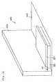
- Fig. 4 is a perspective view of a polarization beam splitter array 320 produced in this manner.
- the polarization beam splitter array 320 has the configuration obtained by alternately joining first and second transparent members 321, 322 having the shape of columns of parallelogram section.
- Fig. 5(A) is a plan sectional view showing a polarization converting element obtained by providing ⁇ /2 optical phase plates at selective portions of the exit surface of the polarization beam splitter array 320 of the embodiment.
- Fig. 5(B) is a plan sectional view showing a polarization converting element which is a control example.
- the ⁇ /2 optical phase plates 381 are attached on the exit surface of the second transparent members 322.
- the ⁇ /2 optical phase plates 381 function as polarization direction converting means.
- the structure of the control example shown in Fig. 5(B) differs from that of the embodiment of Fig. 5(A) only in the point that the positional relationship between the polarization splitting films 331 and the adjacent optical adhesive layers 325 is reversed.
- the polarization beam splitter array 320a shown as a control example first, the reflecting films 332 are formed on the surfaces of the first transparent members 321 and the polarization splitting films 331 are formed on the surfaces of the second transparent members 322.
- the transparent members 321, 322 are then alternately adhered by the optical adhesive layers 325.
- Light having random polarization directions and including an S polarized light component and a P polarized light component enters from the incident surface of the polarization converting element of the embodiment shown in Fig. 5(A).
- the incident light is first separated into S polarized light and P polarized light by the polarization splitting film 331.
- the S polarized light is reflected at substantially a right angle by the polarization splitting film 331, is further reflected by the reflecting film 332, and exits from the exit surface 326.
- the P polarized light passes straight through the polarization splitting film 331, is converted to S polarized light by the ⁇ /2 optical phase plate 381, and exits therefrom. Therefore, only S polarized light is selectively emitted from the polarization converting element.
- ⁇ /2 optical phase plates 381 are selectively provided on the exit surface portions of the first transparent members 321, only P polarized light will be selectively emitted from the polarization converting element.
- the P polarized light passing through the polarization splitting film 331 passes through an optical adhesive layer 325 once in the path from the incident surface of the polarization beam splitter array 320 to the exit surface thereof.
- the S polarized light reflected by the polarization splitting film 331 does not pass through an optical adhesive layer 325 in the path from the incident surface of the polarization beam splitter array 320 to the exit surface thereof.
- the S polarized light passes through two optical adhesive layers 325 in the path from the incident surface of the polarization beam splitter array 320a to the exit surface thereof. While the optical adhesive layer 325 is almost completely transparent, it nevertheless absorbs some amount of light. Each time the light passes through an optical adhesive layer 325, therefore, the light quantity decreases. There is also some possibility of the polarization direction changing somewhat during transmission through the optical adhesive layer 325.
- the light utilization efficiency of the polarization beam splitter array according to the embodiment is higher than that of the control example because the number of passages of the S polarized light through optical adhesive layers 325 is smaller than in the control example.
- the polarization beam splitter array 320a has a relatively high light utilization efficiency because it has fewer optical adhesive layers.
- the light utilization efficiency of the embodiment shown in Fig. 5(A) adds a further improvement in light utilization efficiency beyond that of the control example.
- Fig. 10 is an enlarged sectional view showing the polarization beam splitter array 320 according to the embodiment in further detail.
- the polarization splitting film 331 and the reflecting film 332 have thicknesses of several micrometers ( ⁇ m), which are negligible in comparison with the thicknesses t 321 , t 322 of the transparent members 321, 322 and the thicknesses t ad1 , t ad2 of the optical adhesive layers 325.
- the polarization splitting film 331 is represented by a single broken line and the reflecting film 332 by a single solid line.
- the polarization splitting film 331 and the reflecting film 332 are formed on opposite surfaces of the first transparent member 321.
- the thicknesses t ad1, t ad2 of the optical adhesive layers 325 may be given different values depending on the layer position. In this embodiment, their values t ad1, t ad2 are equal throughout the polarization beam splitter array 320. The following explanation assumes that the thicknesses t ad1, t ad2 of the optical adhesive layers 325 are set at the same value t ad .
- the thickness t 322 of the second transparent member 322 is obtained by subtracting twice the thickness t ad of the optical adhesive layer 325 from the thickness t 321 of the first transparent member 321. This relationship also holds for thicknesses L 321 , L 322 , L ad when the measurement is made along the exit surface 326 or the incident surface 327 of the polarization beam splitter array 320.
- the thickness t 321 of the first transparent member 321 is 3.17 mm.
- the thickness t 322 of the second transparent member 322 is in the range of 3.15 to 2.57 mm.
- the thickness t 322 of the second transparent member 322 is preferably set in the range of about 80% to 90% of the thickness t 321 of the first transparent member 321.
- the interval between the polarization splitting film 331 and the reflecting film 332 after adhesion can be made substantially uniform throughout the polarization beam splitter array 320.
- Fig. 11 is a sectional view showing a condenser lens array 310 consisting of a plurality of condenser lenses 311 arranged in a matrix provided on the incident surface side of the polarization beam splitter array 320.
- the incident surface of the polarization beam splitter array 320 is divided into alternate effective incident areas EA where light is received by the polarization splitting films 331 and converted into effective polarized light (incident areas corresponding to the polarization splitting film 331) and ineffective incident areas UA where light is received by the reflecting films 332 and converted into ineffective polarized light (incident areas corresponding to the reflecting films 332).
- the x-direction width Wp of the effective incident areas EA and the ineffective incident areas UA is equal to half the x-direction width WL of the lenses 311.
- the centers (optical axes) 311c of the lenses 311 are disposed to coincide with the centers of the effective incident areas EA in the x direction.
- the effective incident areas EA correspond to the regions of the polarization splitting films 331 projected onto the incident surface of the polarization beam splitter array 320.
- the pitch of the polarization splitting films 331 in the x direction is thus set to be the same as the pitch of the centers 311c of the lenses 311 in the x direction.
- the lens 311 at the far right in Fig. 11 is not formed with an associated polarization splitting film 331 or reflecting film 332. This is because the absence of these films has little effect on the light utilization efficiency since the light quantity passing through the lens 311 at the end portion is relatively small.
- Figs. 12(a)-12(c) are explanatory diagrams showing the case where the pitch of the polarization splitting films 331 is set to a different value from the pitch of the centers 311c of the lenses 311 and where two polarizing light beam splitters 320' are symmetrically disposed on opposite sides of the system optical axis L so that their polarization splitting films 331 and reflecting films 332 face each other.
- the portion to the left of the system optical axis is not shown in the drawing.
- the quantity distribution of the light collected by the lenses La-Ld of the condenser lens array 310 and received by the incident surface of the polarizing light beam splitter 320' is shown at the middle row in Fig. 12.
- the intensity Ia of the light collected by the lens La which is closest to the system optical axis (the center of the polarizing light beam splitters 320') is strongest and the intensities of the light collected by the other lenses are weaker with increasing distance of the lens from the system optical axis.
- the intensity Id of light collected by the fourth lens Ld is weakest.
- the light quantity distribution of a specific lens (the third lens Lc in Fig.
- the light quantity distribution Pc of the lens Lc is substantially symmetrical relative to the lens center, while the light quantity distributions Pb, Pa of the lenses Lb and La are progressively offset toward the system optical axis with increasing proximity of the lens to the system optical axis.
- the light quantity distribution Pd of the lens Ld is offset away from the system optical axis.
- the centers of the effective incident areas EA of the polarizing light beam splitters 320' are therefore preferably arranged in accordance with the distribution of the light exiting from the condenser lens array 310, i.e., in accordance with the intervals between the light quantity distribution peaks of the light exiting from the condenser lens array 310.
- the thicknesses t 321 , t 322 of the transparent members 321, 322 and the thickness t ad of the optical adhesive layers 325 are preferably adjusted to align the spacing of the polarization splitting films 331 with the spacing of the light quantity distribution peaks.
- an arrangement is preferably adopted where the utilization of the light collected by a lens increases as the lens comes closer to the system optical axis.
- the center of the effective incident area EA1 of the polarizing light beam splitter 320' nearest the optical axis of the light source is preferably aligned substantially with the peak of the light distribution Pa.
- the width of the effective incident areas EA1-EA4 and the ineffective incident areas UA1-UA4 is matched to the intensity distribution or quantity distribution of the light exiting from the condenser lenses 311 of the condenser lens array 310.
- the x-direction width Wp' of the effective incident areas EA (EA1-EA4 in Fig. 12(c)) and the ineffective incident areas UA (UA1-UA4 in Fig. 12(c)) of the polarizing light beam splitter 320' is larger than half the x-direction width WL of the lenses La-Ld of the condenser lens array 310.
- the polarizing light beam splitter 320' is positioned so that the center of the third lens Lc is aligned with the center of the corresponding effective incident area EA3. Since the width of the ineffective incident areas UA is ordinarily equal to the width Wp' of the effective incident areas EA, the two effective incident areas EA2, EA1 on the left side are progressively offset toward the system optical axis relative to the centers of the lenses Lb, La. The center of the rightmost effective incident area EA4 is offset away from the system optical axis relative to the center of the lens Ld.
- the effective incident areas EA1-EA4 are therefore substantially aligned with the peaks of the light quantity distribution of the light exiting from the condenser lens array 310.
- the effective incident areas associated with a prescribed number of lenses, e.g., two or three lenses, near the system optical axis, where the light intensity is particularly high, are preferably aligned substantially with the light quantity distributions of the light collected by these lenses. Use of this arrangement increases the light utilization efficiency.
- the degree to which the width of the effective incident areas EA should be made larger than half the lens width and the selection of the lens whose associated effective incidence area is to be used as the reference for the layout can be easily determined empirically from the number of lenses of the lens array and the light distribution associated with the individual lenses.
- the width of the effective and ineffective incidence areas is not limited to larger than half the lens width. It can be otherwise decided based on the actual quantity distribution of the light received by the incident surface of the polarizing light beam splitter 320'.
- Fig. 13(A) is a plan view showing a condenser lens array 310' having plural types of small lenses differing in size and Fig. 13(B) is sectional taken along line B-B in Fig. 13(A).
- the broken-line circle in Fig. 13(A) designates a region where the quantity of light from the light source is relatively large.
- the condenser lens array 310' has first small lenses 312 of relatively large size arranged in a matrix around the system optical axis L and second small lenses 313 of relatively small size arranged in an approximately matrix configuration near edges of the condenser lens array 310'.
- first small lenses 312 of relatively large size arranged in a matrix around the system optical axis L
- second small lenses 313 of relatively small size arranged in an approximately matrix configuration near edges of the condenser lens array 310'.
- the thicknesses t 321 , t 322 of the transparent members 321, 322 and the thickness t ad of the optical adhesive layers 325 are adjusted so as to align the centers of the effective incidence areas of the polarization beam splitter array (i.e., the pitch of the polarization splitting films) with the pitches of the light quantity distributions of the beams exiting from the associated small lenses 312, 313.
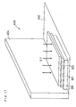
- Figs. 14 to 19 are explanatory diagrams showing a method for fabricating a polarization beam splitter array according to a second embodiment. As shown in Fig. 14, the second embodiment uses a horizontal table 402 and a vertical wall 404 standing on the horizontal table 402.
- the first transparent members 321 (glass plates with films) and the second transparent members 322 (glass plates without films) shown in Fig. 2(A) are prepared.
- the dummy glass plate 324 shown in Fig. 14 is also made ready.
- the dummy glass plate 324 is a flat plate of glass which is not provided with a polarization splitting film or a reflecting film.
- the dummy glass plate 324 constitutes an end of the polarization beam splitter.
- the thickness of the dummy glass plate 324 may be set different from those of the first and second transparent members 321, 322.
- the state of Fig. 14 is obtained by first placing the dummy glass plate 324 on the horizontal table 402 and coating its upper surface with a photo-curing adhesive, then placing the first transparent member 321 on the dummy glass plate 324.
- the dummy glass plate 324 and the first transparent member 321 stacked with the adhesive layer therebetween are rubbed together to drive air bubbles out of the adhesive layer and even the thickness of the adhesive layer.
- the dummy glass plate 324 and the first transparent member 321 adhere to each other owing to surface tension.
- the dummy glass plate 324 and the first transparent member 321 abut on the vertical wall 404.
- the dummy glass plate 324 and the first transparent member 321 are offset by a prescribed offset distance ⁇ H at the surfaces perpendicular to the abutting surfaces.
- ultraviolet rays (UV in the figure) are projected onto the first transparent member 321 from above to cure the adhesive.
- the plate members adhered in this manner are called the "first stack.”
- the ultraviolet rays are preferably projected from a direction that is not parallel to the surface of the first transparent member 321.
- the adhesive can be efficiently irradiated by ultraviolet rays projected in this manner, thereby shortening the adhesive curing time and improving the optical element production throughput.
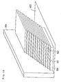
- the upper surface of the first stack is coated with adhesive and the second transparent member 322 is placed thereon (Fig. 16).
- the first and second transparent members 321, 322 stacked with the adhesive layer therebetween are rubbed together to drive air bubbles out of the adhesive layer and even the thickness of the adhesive layer.
- the first transparent member 321 and the second transparent member 322 are offset by the prescribed offset distance ⁇ H.
- ultraviolet rays are projected onto the second transparent member 322 from above to cure the adhesive. A second stack is thus obtained.
- the aforesaid process of applying an adhesive layer, overlaying a transparent member and projecting ultraviolet rays thereon to cure the adhesive layer is then repeated to obtain the stack shown in Fig. 18.
- This stack is then cut as shown in Fig. 19.
- the cutting is conducted with the side of the stack shown in abutment with the vertical wall 404 in Fig. 18 facing downward and resting on a cutting table 410. It is cut along parallel cutting lines 328a, 328b.
- An element similar to the polarization beam splitter array of the first embodiment shown in Fig. 4 is then obtained by polishing the cut surfaces until flat.
- the polarization beam splitter array according to the second embodiment is different, however, in that it has the dummy glass plate 324 at the end thereof.
- the polarization beam splitter array of the first embodiment can also be assembled by the assembly method of the second embodiment.
- unit stacks each obtained by bonding together a single first transparent member 321 and a single second transparent member 322 in the manner of the second embodiment and then successively laminating the unit stacks.
- one unit stack can be laminated to sandwich an adhesive layer, the air bubbles be driven out of the adhesive layer, and the adhesive layer then be cured by irradiation with ultraviolet rays.
- the thickness precision of the transparent members 321, 322 can be controlled at the time of polishing their surfaces.
- Adhesive layers of uniform thickness can be obtained by applying the adhesive to a uniform coating weight throughout the member surfaces and applying pressure evenly to the member surface in the step of driving out air bubbles.
- Fig. 6 is a schematic structural plan view of the essential portion of a polarized light illumination system 1 including a polarization beam splitter array which is an embodiment of this invention described in the foregoing.
- the polarized light illumination system 1 is equipped with a light source section 10 and a polarized light generator 20.
- the light source section 10 emits a light beam having random polarization directions and including an S polarized light component and a P polarized light component.
- the light beam emitted by the light source section 10 is converted to a single type of linearly polarized light generally aligned in one polarization direction by the polarized light generator 20.
- the linearly polarized light from the polarized light generator 20 illuminates an illumination area 90.
- the light source section 10 comprises a lamp 101 and a parabolic reflector 102.
- the light emitted by the lamp 101 is reflected in one direction by the parabolic reflector 102 and passes to the polarized light generator 20 as a generally parallel beam.
- the optical axis R of the light source section 10 is shifted parallel to the system optical axis L in the x direction by a given distance D.
- the system optical axis L is the optical axis of a polarization beam splitter array 320. The reason for shifting the light source optical axis R will be described later.
- the polarized light generator 20 comprises a first optical element 200 and a second optical element 300.
- Fig. 7 is a perspective view of the first optical element 200.
- the first optical element 200 is made of a plurality of small beam dividing lenses 201 of rectangular profile arrayed vertically and horizontally in the form of a square matrix.
- the first optical element 200 is disposed so that the light source optical axis R (Fig. 6) is aligned with the center of the first optical element 200.
- the profiles of the individual beam dividing lenses 201 as viewed in the z direction are made similar to that of the illumination area 90. Since this embodiment assumes an illumination area 90 that is long in the x direction, the beam dividing lenses 201 also have an xy surface that is long in the lateral (x) direction.
- the second optical element 300 in Fig. 6 comprises a condenser lens array 310, a polarization beam splitter array 320, a selective phase plate 380 and an exit side lens 390.
- the selective phase plate 380 is a platelike member including ⁇ /2 optical phase plates 381 which, as explained with reference to Fig. 5, are formed only at the exit surface portions of the second transparent member 322, and the other parts of the selective phase plate 380 located at the exit surface portions of the first transparent member 321is colorless and transparent.
- the polarization beam splitter array shown in Fig. 6 has the approximate shape of a rectangular parallelopiped obtained by cutting off the projecting portions at the opposite edges of the structure shown in Fig. 4.
- the condenser lens array 310 is of substantially the same structure as the first optical element 200 shown in Fig. 7. Specifically, the condenser lens array 310 is made of a matrix of condenser lenses 311 in a number equal to the number of beam dividing lenses 201 of the first optical element 200 The center of the condenser lens array 310 is also aligned with the light source optical axis R.
- the light source section 10 emits a substantially parallel beam of white light having random polarization directions.
- the light beam emitted by the light source section 10 and entering the first optical element 200 is divided into intermediate beams 202 by the beam dividing lenses 201.
- the condensing action of the beam dividing lenses 201 and the condenser lenses 311 converges the intermediate beams 202 in the plane perpendicular to the system optical axis L (the xy plane in Fig. 6).
- Light source images are formed in a number equal to the number of beam dividing lenses 201 at the positions where the intermediate beams 202 converge.
- the light source images are formed at positions near the polarization splitting films 331 in the polarization beam splitter array 320.
- the offsetting of the light source optical axis R from the system optical axis L is intended to enable formation of light source images at the positions of the polarization splitting films 331.
- the offset distance D is set at half the x-direction width Wp (Fig. 6) of the polarization splitting film 331.
- the centers of the polarization splitting films 331 for splitting the intermediate beams 202 are also offset by Wp/2 relative to the system optical axis L.
- the offsetting of the light source optical axis R from the system optical axis L by Wp/2 therefore enables light source images (images of the lamp 101)to be formed substantially at the centers of the polarization splitting films 331.
- the beams entering the polarization beam splitter array 320 are entirely converted to S polarized light.
- the beams exiting the polarization beam splitter array 320 pass through the exit side lens 390 and illuminate the illumination area 90. Since the illumination area 90 is illuminated by a large number of beams produced by the beam dividing lenses 201, it is evenly illuminated throughout.
- the condenser lens array 310 can be omitted from the second optical element 300.
- the polarized light illumination system 1 shown in Fig. 6 functions as a polarized light generator capable of converting a beam of white light having random polarization directions into a light beam having a specific polarization direction (S polarized light or P polarized light) and further functions as an illuminator capable of evenly illuminating the illumination area 90 with a large number of polarized light beams. Since the polarized light illumination system 1 uses the polarization beam splitter array 320, which is an embodiment of this invention, it provides higher light utilization efficiency than achievable by the prior art.
- Fig. 8 is a schematic structural view showing the essential portion of a projection display system 800 equipped with the polarized light illumination system 1 shown in Fig. 6.
- the projection display system 800 comprises the polarized light illumination system 1, dichroic mirrors 801, 804, reflecting mirrors 802, 807, 809, relay lenses 806, 808, 810, three liquid crystal panels (liquid crystal light valves) 803, 805, 811, a cross dichroic prism 813 and a projection lens 814.
- the dichroic mirrors 801, 804 function as color separating means for separating a white light beam into three colors: red, blue and green.
- the three liquid crystal panels 803, 805, 811 function as light modulating means for forming images by modulating the light of each of the three colors according to supplied image information (image signals).
- the cross dichroic prism 813 functions as a color combining means for combining the red, blue and green light to form a color image.
- the projection lens 814 functions as a projection optical system for projecting the light representing the combined image on a screen 815.
- the blue- and green-reflecting dichroic mirror 801 transmits the red light component of the white light beam emitted from the polarized light illumination system 1 and reflects the blue light component and the green light component thereof.
- the transmitted red light is reflected by the reflecting mirror 802 and passes to the red liquid crystal panel 803.
- the green light reflected by the first dichroic mirror 801 is reflected by the green-reflecting dichroic mirror 804 and passes to the green liquid crystal panel 805.
- the blue light reflected by the first dichroic mirror 801 passes through the second dichroic mirror 804.
- the optical path length of the blue light is longest among the three colors.
- the blue light After the blue light has passed through the dichroic mirror 804, it enters a light guide means 850 including an entrance lens 806, a relay lens 808 and an exit lens 810.
- the blue light transmitted through the dichroic mirror 804 passes through the entrance lens 806, is reflected by the reflecting mirror 807 and passes to the relay lens 808. It is then reflected by the reflecting mirror 809, through the exit lens 810 and to the blue liquid crystal panel 811.
- the three liquid crystal panels 803, 805 and 811 correspond to the illumination area 90 in Fig. 6.
- the three liquid crystal panels 803, 805, 811 modulate the light of each color in accordance with an image signal (image information) supplied from external control circuits (not shown) to produce colored light carrying image information of the color component concerned.
- the modulated red, blue and green lights enter the cross dichroic prism 813.
- the cross dichroic prism 813 is formed with multi-layer dielectric film stacks which reflect red light and multi-layer dielectric film stacks which reflect blue light arranged in the form of a cross.
- the three colors are merged by these multi-layer dielectric film stacks into light carrying a color image.
- the merged light is projected on the screen 815 by the projection lens 814 constituting the projection system to display an enlarged image.
- the liquid crystal panels 803, 805, 811 used as light modulating means in the projection display system 800 are of the type which modulate light beams of a specific polarization direction (S polarized light or P polarized light). These liquid crystal display panels ordinarily have polarizing plates (not shown) attached to their incident and exit surfaces. When such a liquid crystal display panel is illuminated with a light beam having random polarization directions, therefore, about half of the light beam will be absorbed by the polarizing plates and changed to heat. The light utilization efficiency will be therefore low. In addition, the polarizing plates will generate much heat, which will also cause problems. In the projection display system 800 shown in Fig.
- the polarized light illumination system 1 generates light beams of the specific polarization direction for passage through the liquid crystal panels 803, 805, 811.
- the problem of absorption of light and generation of heat at the polarizing plates of the liquid crystal display panels is therefore greatly alleviated.
- the projection display system 800 uses the polarization beam splitter array 320, which is an embodiment of the invention, it also enjoys a corresponding improvement in overall light utilization efficiency.
- the reflecting films 332 of the polarization beam splitter array 320 are preferably formed as multi-layer dielectric film stacks with the property of selectively reflecting only the specific polarized light component (e.g. S polarized light) to be modulated by the liquid crystal panels 803, 805, 811. This is advantageous because it further mitigates the problem of light absorption and heat generation at the liquid crystal panels 803, 805, 811. This in turn enhances the overall light utilization efficiency of the projection display system 800.
- the specific polarized light component e.g. S polarized light
- the projection display system can achieve an improvement in light utilization efficiency over the prior art.
- the images projected on the screen 815 are therefore brighter.
- the polarization beam splitter array of the invention can also be applied to various systems and devices other than the projection display system shown in Fig. 8.
- the polarization beam splitter array can be applied to a projection display system for projecting monochrome images instead of color images.
- the system of Fig. 8 requires only a single liquid crystal display panel, while the color separating means for three-color separation and the color synthesizing means for synthesizing light of three colors can be omitted.
- a light shielding means can be provided to prevent entry of light from the incident surface of the second transparent members.
- Fig. 9(A) is an explanatory diagram showing how a light shielding plate 340 is provided in front of the optical element according to the embodiment of Fig. 5(A).
- the light shielding plate 340 alternately includes light shielding portions 341 for shutting out light and transparent portions 342 for passing light.
- the light shielding plate 340 can be fabricated by, for example, forming light absorbing films or light reflecting films as the light shielding portions 341 on the surface of a glass plate or other transparent plate member.
- the light shielding portions 341 are provided in association with the incident surface 327 of the second transparent members 322 so as to shield the incident surface 327.
- Fig. 9(B) shows the optical path of the light entering from the incident surface 327 of the second transparent member 322 when the light shielding plate 340 is not provided.
- the light entering from the incident surface 327 is reflected by the reflecting film 322a and is then split into S polarized light and P polarized light by the polarization splitting film 331 thereabove.
- the P polarized light is converted into S polarized light by the ⁇ /2 optical phase plate 381.
- the S polarized light is reflected by the reflecting film 332b above the polarization splitting film 331 and exits through the exit surface 326.
- the S polarized light component of the light entering through the incident surface 327 passes through the first optical adhesive layer 325a twice and then through the optical adhesive layer 325b once before reaching the reflecting film 332b above.
- the P polarized light component passes through the optical adhesive layer 325a twice and the optical adhesive layer 325b twice before reaching the ⁇ /2 optical phase plate 381.
- the light shielding plate 340 is not provided, therefore, the light entering through the incident surface 327 of the second transparent member 322 passes repeatedly through optical adhesive layers 325. This light can be shut out by providing the light shielding plate 340 as shown in Fig. 9(A).
Applications Claiming Priority (8)
| Application Number | Priority Date | Filing Date | Title |
|---|---|---|---|
| JP21537796 | 1996-07-25 | ||
| JP21537796 | 1996-07-25 | ||
| JP21537896 | 1996-07-25 | ||
| JP8215378A JPH1039136A (ja) | 1996-07-25 | 1996-07-25 | 光学素子および投写型表示装置 |
| JP35521096 | 1996-12-19 | ||
| JP35521096A JP3486516B2 (ja) | 1996-07-25 | 1996-12-19 | 光学素子 |
| EP97305527A EP0821258B1 (fr) | 1996-07-25 | 1997-07-23 | Elément optique pour dispositif d'affichage par projection |
| EP00202160A EP1055955B1 (fr) | 1996-07-25 | 1997-07-23 | Elément optique pour dispositif d'affichage par projection |
Related Parent Applications (1)
| Application Number | Title | Priority Date | Filing Date |
|---|---|---|---|
| EP00202160A Division EP1055955B1 (fr) | 1996-07-25 | 1997-07-23 | Elément optique pour dispositif d'affichage par projection |
Publications (2)
| Publication Number | Publication Date |
|---|---|
| EP1231499A2 true EP1231499A2 (fr) | 2002-08-14 |
| EP1231499A3 EP1231499A3 (fr) | 2002-08-21 |
Family
ID=27329751
Family Applications (4)
| Application Number | Title | Priority Date | Filing Date |
|---|---|---|---|
| EP02010138A Expired - Lifetime EP1231498B1 (fr) | 1996-07-25 | 1997-07-23 | Dispositif optique d'illumination pour dispositif d'affichage par projection |
| EP00202160A Expired - Lifetime EP1055955B1 (fr) | 1996-07-25 | 1997-07-23 | Elément optique pour dispositif d'affichage par projection |
| EP02010139A Withdrawn EP1231499A3 (fr) | 1996-07-25 | 1997-07-23 | Elément optique pour dispositif d'affichage par projection |
| EP97305527A Expired - Lifetime EP0821258B1 (fr) | 1996-07-25 | 1997-07-23 | Elément optique pour dispositif d'affichage par projection |
Family Applications Before (2)
| Application Number | Title | Priority Date | Filing Date |
|---|---|---|---|
| EP02010138A Expired - Lifetime EP1231498B1 (fr) | 1996-07-25 | 1997-07-23 | Dispositif optique d'illumination pour dispositif d'affichage par projection |
| EP00202160A Expired - Lifetime EP1055955B1 (fr) | 1996-07-25 | 1997-07-23 | Elément optique pour dispositif d'affichage par projection |
Family Applications After (1)
| Application Number | Title | Priority Date | Filing Date |
|---|---|---|---|
| EP97305527A Expired - Lifetime EP0821258B1 (fr) | 1996-07-25 | 1997-07-23 | Elément optique pour dispositif d'affichage par projection |
Country Status (6)
| Country | Link |
|---|---|
| US (3) | US6404550B1 (fr) |
| EP (4) | EP1231498B1 (fr) |
| KR (1) | KR100523874B1 (fr) |
| CN (1) | CN1132029C (fr) |
| DE (3) | DE69734251T2 (fr) |
| TW (1) | TW393586B (fr) |
Families Citing this family (108)
| Publication number | Priority date | Publication date | Assignee | Title |
|---|---|---|---|---|
| US6404550B1 (en) * | 1996-07-25 | 2002-06-11 | Seiko Epson Corporation | Optical element suitable for projection display apparatus |
| JP3298437B2 (ja) | 1996-12-18 | 2002-07-02 | セイコーエプソン株式会社 | 光学素子、偏光照明装置および投写型表示装置 |
| US6995917B1 (en) | 1999-04-08 | 2006-02-07 | Sharp Laboratories Of America, Inc. | Projection display system using polarized light |
| TW455705B (en) | 1999-07-05 | 2001-09-21 | Seiko Epson Corp | Manufacturing method of polarization transformation element |
| JP2001021719A (ja) | 1999-07-12 | 2001-01-26 | Seiko Epson Corp | 偏光分離素子、偏光変換素子および投写型表示装置 |
| JP2001100029A (ja) * | 1999-09-29 | 2001-04-13 | Fujitsu General Ltd | 偏光カラーフィルタ及びこのフィルタを用いた映像投影装置 |
| US6781640B1 (en) | 1999-11-15 | 2004-08-24 | Sharp Laboratories Of America, Inc. | Projection display having polarization compensator |
| JP2001343512A (ja) | 2000-05-31 | 2001-12-14 | Canon Inc | 回折光学素子及びそれを有する光学系 |
| JP2002182158A (ja) * | 2000-12-12 | 2002-06-26 | Ushio Inc | 偏光ビームスプリッタを備えた光配向用偏光光照射装置 |
| US6511183B2 (en) * | 2001-06-02 | 2003-01-28 | Koninklijke Philips Electronics N.V. | Digital image projector with oriented fixed-polarization-axis polarizing beamsplitter |
| DE10127621A1 (de) | 2001-06-07 | 2002-12-12 | Zeiss Carl Jena Gmbh | Anordnung zum Projizieren eines Bildes auf eine Projektionsfläche |
| DE10127620A1 (de) | 2001-06-07 | 2002-12-12 | Zeiss Carl Jena Gmbh | Anordnung zum Projizieren eines mehrfarbigen Bildes auf eine Projektionsfläche |
| DE10127617A1 (de) | 2001-06-07 | 2002-12-12 | Zeiss Carl Jena Gmbh | Projektionsanordnung |
| JP2003014932A (ja) | 2001-06-29 | 2003-01-15 | Canon Inc | 偏光ビームスプリッタ、および偏光ビームスプリッタの作成方法 |
| US6949297B2 (en) * | 2001-11-02 | 2005-09-27 | 3M Innovative Properties Company | Hybrid adhesives, articles, and methods |
| US6860607B2 (en) * | 2002-03-15 | 2005-03-01 | Seiko Epson Corporation | Integrator type illumination optical system and projector having the same |
| TWI240841B (en) * | 2002-06-10 | 2005-10-01 | Reveo Inc | Scalable and mass-manufacturable OXC using liquid crystal cells |
| US6887917B2 (en) * | 2002-12-30 | 2005-05-03 | 3M Innovative Properties Company | Curable pressure sensitive adhesive compositions |
| US7927703B2 (en) * | 2003-04-11 | 2011-04-19 | 3M Innovative Properties Company | Adhesive blends, articles, and methods |
| US20040263974A1 (en) * | 2003-06-26 | 2004-12-30 | Optical Coating Laboratory Inc., A Jds Unipahse Company And A Corporation Of The State Of Delware | Flat polarization conversion system with patterned retarder |
| US20050041288A1 (en) * | 2003-08-19 | 2005-02-24 | Liao Liu Liang | Polarization conversion module and polarization conversion method thereof |
| US7234816B2 (en) * | 2004-02-03 | 2007-06-26 | 3M Innovative Properties Company | Polarizing beam splitter assembly adhesive |
| CN1301419C (zh) * | 2004-03-22 | 2007-02-21 | 昂纳信息技术(深圳)有限公司 | 多激光光束复合装置 |
| US7561323B2 (en) * | 2004-09-27 | 2009-07-14 | Idc, Llc | Optical films for directing light towards active areas of displays |
| IL166799A (en) * | 2005-02-10 | 2014-09-30 | Lumus Ltd | Aluminum shale surfaces for use in a conductive substrate |
| US10073264B2 (en) | 2007-08-03 | 2018-09-11 | Lumus Ltd. | Substrate-guide optical device |
| GB2425846A (en) * | 2005-04-20 | 2006-11-08 | Bookham Technology Plc | Multi component beam splitter with individual surface coatings |
| JP5030134B2 (ja) * | 2005-08-18 | 2012-09-19 | 株式会社リコー | 偏光変換素子、偏光変換光学系および画像投影装置 |
| KR100634550B1 (ko) * | 2005-08-24 | 2006-10-16 | 삼성전자주식회사 | 편광변환시스템 및 그 제조 방법 및 이를 적용한액정표시장치 |
| US10261321B2 (en) | 2005-11-08 | 2019-04-16 | Lumus Ltd. | Polarizing optical system |
| IL171820A (en) * | 2005-11-08 | 2014-04-30 | Lumus Ltd | A polarizing optical component for light coupling within a conductive substrate |
| JP5226528B2 (ja) | 2005-11-21 | 2013-07-03 | マイクロビジョン,インク. | 像誘導基板を有するディスプレイ |
| US20070229765A1 (en) * | 2006-03-30 | 2007-10-04 | Infocus Corporation | Projection system and method |
| CN101241190B (zh) * | 2007-04-25 | 2011-05-11 | 中国科学院安徽光学精密机械研究所 | 基于泽尼克模式的激光大气湍流强度廓线测量系统和方法 |
| US7589901B2 (en) * | 2007-07-10 | 2009-09-15 | Microvision, Inc. | Substrate-guided relays for use with scanned beam light sources |
| US8279523B2 (en) * | 2007-08-22 | 2012-10-02 | Seiko Epson Corporation | Polarization conversion element and method for manufacturing the same |
| TWI391708B (zh) * | 2007-12-25 | 2013-04-01 | Ind Tech Res Inst | 極化色彩分光裝置 |
| CN101546045B (zh) * | 2008-03-28 | 2012-08-15 | 红蝶科技(深圳)有限公司 | 偏振转换装置及使用其的投影系统 |
| CN101576630B (zh) * | 2008-05-06 | 2012-11-14 | 红蝶科技(深圳)有限公司 | 预偏振器及液晶投影系统 |
| JP5334494B2 (ja) * | 2008-08-20 | 2013-11-06 | 三菱電機株式会社 | 投写型表示装置 |
| CN101366537B (zh) * | 2008-08-26 | 2011-12-28 | 三门县琴海水产养殖有限公司 | 醉制青蟹及其加工方法 |
| JP2010140888A (ja) * | 2008-11-14 | 2010-06-24 | Seiko Epson Corp | 照明装置、プロジェクタ |
| JP5195354B2 (ja) * | 2008-12-01 | 2013-05-08 | セイコーエプソン株式会社 | 光学素子 |
| US8867133B2 (en) * | 2009-07-06 | 2014-10-21 | Lg Innotek Co., Ltd. | Polarization converting device and method for manufacturing the same |
| US8698705B2 (en) * | 2009-12-04 | 2014-04-15 | Vuzix Corporation | Compact near eye display with scanned image generation |
| CN102906625A (zh) * | 2010-05-19 | 2013-01-30 | 3M创新有限公司 | 蝇眼积分器偏振转换器 |
| TWI406011B (zh) * | 2010-06-18 | 2013-08-21 | Univ Nat Taipei Technology | 可增強光線中某一偏極態之光學系統與具有此系統之光源系統 |
| JP5541056B2 (ja) * | 2010-10-01 | 2014-07-09 | セイコーエプソン株式会社 | 偏光変換素子、偏光変換ユニット、投射装置、及び偏光変換素子の製造方法 |
| US8531773B2 (en) | 2011-01-10 | 2013-09-10 | Microvision, Inc. | Substrate guided relay having a homogenizing layer |
| US8391668B2 (en) | 2011-01-13 | 2013-03-05 | Microvision, Inc. | Substrate guided relay having an absorbing edge to reduce alignment constraints |
| JP5919622B2 (ja) * | 2011-01-21 | 2016-05-18 | セイコーエプソン株式会社 | 偏光変換素子、偏光変換ユニット及び投写型映像装置 |
| TW201303375A (zh) * | 2011-07-08 | 2013-01-16 | Asia Optical Co Inc | 光學極性轉換系統 |
| CN105301882A (zh) * | 2011-09-07 | 2016-02-03 | 精工爱普生株式会社 | 投影机 |
| JP5953835B2 (ja) * | 2011-09-07 | 2016-07-20 | セイコーエプソン株式会社 | プロジェクター |
| CN103376633B (zh) * | 2012-04-17 | 2015-06-24 | 台达电子工业股份有限公司 | 一种用于投影装置的光源系统及投影装置 |
| DE102012210808B4 (de) * | 2012-06-26 | 2018-05-17 | Sypro Optics Gmbh | Head-up Display und Projektionsoptik für ein Head-up Display |
| KR20150024416A (ko) * | 2012-06-27 | 2015-03-06 | 쓰리엠 이노베이티브 프로퍼티즈 컴파니 | 광학 컴포넌트 어레이 |
| WO2014167904A1 (fr) * | 2013-04-12 | 2014-10-16 | シャープ株式会社 | Elément formant image de type réfléchissant et procédé de fabrication d'élément formant image de type réfléchissant |
| WO2014208725A1 (fr) | 2013-06-27 | 2014-12-31 | デクセリアルズ株式会社 | Élément de conversion de polarisation, procédé de fabrication d'élément de conversion de polarisation, et dispositif optique |
| US10042176B2 (en) | 2013-06-27 | 2018-08-07 | Dexerials Corporation | Polarization conversion element, polarization-conversion-element manufacturing method, light-source unit, and optical device |
| JP6287037B2 (ja) * | 2013-10-16 | 2018-03-07 | セイコーエプソン株式会社 | 偏光変換素子、プロジェクター、および偏光変換素子の製造方法 |
| IL232197B (en) | 2014-04-23 | 2018-04-30 | Lumus Ltd | Compact head-up display system |
| IL235642B (en) | 2014-11-11 | 2021-08-31 | Lumus Ltd | A compact head-up display system is protected by an element with a super-thin structure |
| CN107003475B (zh) * | 2014-11-13 | 2020-10-27 | 新加坡恒立私人有限公司 | 光学导光元件的制造 |
| CN106154640B (zh) * | 2015-03-31 | 2020-02-21 | 联想(北京)有限公司 | 显示组件和电子设备 |
| RU2746980C1 (ru) | 2016-10-09 | 2021-04-22 | Лумус Лтд | Умножитель апертуры с использованием прямоугольного волновода |
| RU2763850C2 (ru) | 2016-11-08 | 2022-01-11 | Люмус Лтд | Световодное устройство с краем, обеспечивающим оптическую отсечку, и соответствующие способы его изготовления |
| EP3574360A4 (fr) | 2017-01-28 | 2020-11-11 | Lumus Ltd. | Système d'imagerie à réalité augmentée |
| EP3397998A4 (fr) | 2017-02-22 | 2019-04-17 | Lumus Ltd. | Ensemble optique de guide de lumière |
| WO2018169968A1 (fr) | 2017-03-16 | 2018-09-20 | Invensas Corporation | Réseaux de del à liaison directe et applications |
| KR102501345B1 (ko) | 2017-03-22 | 2023-02-17 | 루머스 리미티드 | 중첩 파셋 |
| IL251645B (en) | 2017-04-06 | 2018-08-30 | Lumus Ltd | Waveguide and method of production |
| WO2019016813A1 (fr) | 2017-07-19 | 2019-01-24 | Lumus Ltd. | Éclairage à cristaux liquides sur silicium par l'intermédiaire d'un élément optique guide de lumière |
| CA3068659A1 (fr) | 2018-01-02 | 2019-07-11 | Lumus Ltd. | Affichages a realite augmentee a alignement actif et procedes correspondants |
| US10551544B2 (en) | 2018-01-21 | 2020-02-04 | Lumus Ltd. | Light-guide optical element with multiple-axis internal aperture expansion |
| US11169326B2 (en) | 2018-02-26 | 2021-11-09 | Invensas Bonding Technologies, Inc. | Integrated optical waveguides, direct-bonded waveguide interface joints, optical routing and interconnects |
| US11256004B2 (en) * | 2018-03-20 | 2022-02-22 | Invensas Bonding Technologies, Inc. | Direct-bonded lamination for improved image clarity in optical devices |
| IL259518B2 (en) | 2018-05-22 | 2023-04-01 | Lumus Ltd | Optical system and method for improving light field uniformity |
| AU2019274687B2 (en) | 2018-05-23 | 2023-05-11 | Lumus Ltd. | Optical system including light-guide optical element with partially-reflective internal surfaces |
| US11415812B2 (en) | 2018-06-26 | 2022-08-16 | Lumus Ltd. | Compact collimating optical device and system |
| US11409103B2 (en) | 2018-07-16 | 2022-08-09 | Lumus Ltd. | Light-guide optical element employing polarized internal reflectors |
| JP7407458B2 (ja) | 2018-09-09 | 2024-01-04 | ルムス エルティーディー. | 二次元の拡張を有する導光光学素子を含む光学システム |
| US11353786B2 (en) | 2018-09-11 | 2022-06-07 | Sony Corporation | Polarizing beam splitter and projector |
| CN109188700B (zh) * | 2018-10-30 | 2021-05-11 | 京东方科技集团股份有限公司 | 光学显示系统及ar/vr显示装置 |
| TW202026685A (zh) | 2018-11-08 | 2020-07-16 | 以色列商魯姆斯有限公司 | 具有反射鏡的光導顯示器 |
| DE102019200193B3 (de) * | 2019-01-09 | 2020-02-06 | Carl Zeiss Smt Gmbh | Optisches System für eine Projektionsbelichtungsanlage |
| WO2020148665A1 (fr) | 2019-01-15 | 2020-07-23 | Lumus Ltd. | Procédé de fabrication d'un élément optique de guide de lumière symétrique |
| CA3123518C (fr) | 2019-01-24 | 2023-07-04 | Lumus Ltd. | Systemes optiques comprenant un loe a expansion a trois etages |
| EP3939246A4 (fr) | 2019-03-12 | 2022-10-26 | Lumus Ltd. | Projecteur d'image |
| KR20210151782A (ko) * | 2019-04-15 | 2021-12-14 | 루머스 리미티드 | 광-유도 광학 소자 제조 방법 |
| MX2021015750A (es) | 2019-06-27 | 2022-01-27 | Lumus Ltd | Aparato y metodos de seguimiento ocular a partir de la obtencion de imagenes oculares mediante un elemento optico de guia de luz. |
| CN114080558A (zh) | 2019-07-04 | 2022-02-22 | 鲁姆斯有限公司 | 具有对称光束倍增的图像波导 |
| TW202127106A (zh) * | 2019-09-04 | 2021-07-16 | 以色列商魯姆斯有限公司 | 具有二向色光束組合器的光學裝置、結合二向色光束組合器使用的光學裝置及其製造方法 |
| CN110673242B (zh) * | 2019-10-14 | 2022-08-26 | 江西师范大学 | 一种偏振可调谐硅基光学吸波器及其制备方法 |
| CN114599480B (zh) | 2019-11-25 | 2024-03-19 | 鲁姆斯有限公司 | 抛光波导表面的方法 |
| IL270991B (en) | 2019-11-27 | 2020-07-30 | Lumus Ltd | A light guide with an optical element to perform polarization mixing |
| BR112022009872A2 (pt) | 2019-12-05 | 2022-08-09 | Lumus Ltd | Dispositivo óptico e método para fabricar um dispositivo óptico |
| EP4042232A4 (fr) | 2019-12-08 | 2022-12-28 | Lumus Ltd. | Système optique avec projecteur d'image compact |
| US11762200B2 (en) | 2019-12-17 | 2023-09-19 | Adeia Semiconductor Bonding Technologies Inc. | Bonded optical devices |
| WO2021137228A1 (fr) | 2019-12-30 | 2021-07-08 | Lumus Ltd. | Systèmes optiques comprenant des éléments optiques de guidage de lumière ayant une expansion bidimensionnelle |
| CN115552171B (zh) | 2020-05-24 | 2024-01-23 | 鲁姆斯有限公司 | 复合光导光学元件的制造方法以及光学结构 |
| KR102638480B1 (ko) | 2020-11-09 | 2024-02-19 | 루머스 리미티드 | 역반사되는 환경의 주변광의 색도를 조절하는 방법 |
| EP4162314A4 (fr) | 2021-02-25 | 2023-11-22 | Lumus Ltd. | Multiplicateurs à ouverture optique ayant un guide d'ondes rectangulaire |
| KR20230148324A (ko) | 2021-03-01 | 2023-10-24 | 루머스 리미티드 | 프로젝터로부터 도파관으로의 콤팩트한 커플링을 갖는광학 시스템 |
| KR20230133841A (ko) | 2021-05-19 | 2023-09-19 | 루머스 리미티드 | 액티브 광학 엔진 |
| CN117425843A (zh) | 2021-06-07 | 2024-01-19 | 鲁姆斯有限公司 | 具有矩形波导的光学孔径倍增器的制造方法 |
| WO2023281499A1 (fr) | 2021-07-04 | 2023-01-12 | Lumus Ltd. | Affichage avec éléments de guide de lumière empilés fournissant différentes parties de champ de vision |
| WO2023026266A1 (fr) | 2021-08-23 | 2023-03-02 | Lumus Ltd. | Procédés de fabrication d'éléments optiques de guide de lumière composés ayant des réflecteurs de couplage incorporés |
Citations (5)
| Publication number | Priority date | Publication date | Assignee | Title |
|---|---|---|---|---|
| DE935663C (de) * | 1950-02-28 | 1955-11-24 | Jenaer Glaswerk Schott & Gen | Lichtquelle fuer polarisiertes Licht |
| US2748659A (en) * | 1951-02-26 | 1956-06-05 | Jenaer Glaswerk Schott & Gen | Light source, searchlight or the like for polarized light |
| EP0359658A2 (fr) * | 1988-09-12 | 1990-03-21 | Fujitsu Limited | Matériau optique de base et produit optique utilisant ce materiau et méthode de fabrication de ce matériau |
| US5096520A (en) * | 1990-08-01 | 1992-03-17 | Faris Sades M | Method for producing high efficiency polarizing filters |
| EP0508413A2 (fr) * | 1991-04-09 | 1992-10-14 | Canon Kabushiki Kaisha | Elément de polarisation en forme de plaque, unité de conversion de polarisation comprenant cet élément, et projecteur comprenant cette unité |
Family Cites Families (25)
| Publication number | Priority date | Publication date | Assignee | Title |
|---|---|---|---|---|
| US3743380A (en) * | 1972-01-31 | 1973-07-03 | Us Navy | Polarized light source for underwater use |
| CH558023A (de) * | 1972-08-29 | 1975-01-15 | Battelle Memorial Institute | Polarisationsvorrichtung. |
| GB2153546A (en) | 1984-02-02 | 1985-08-21 | Pilkington Perkin Elmer Ltd | Optical filtering devices |
| US4709144A (en) | 1986-04-02 | 1987-11-24 | Hewlett-Packard Company | Color imager utilizing novel trichromatic beamsplitter and photosensor |
| US5157526A (en) * | 1990-07-06 | 1992-10-20 | Hitachi, Ltd. | Unabsorbing type polarizer, method for manufacturing the same, polarized light source using the same, and apparatus for liquid crystal display using the same |
| US5751480A (en) | 1991-04-09 | 1998-05-12 | Canon Kabushiki Kaisha | Plate-like polarizing element, a polarizing conversion unit provided with the element, and a projector provided with the unit |
| US5381278A (en) * | 1991-05-07 | 1995-01-10 | Canon Kabushiki Kaisha | Polarization conversion unit, polarization illumination apparatus provided with the unit, and projector provided with the apparatus |
| JPH05241103A (ja) | 1992-02-21 | 1993-09-21 | Nec Corp | 投射型液晶表示装置 |
| JP2773562B2 (ja) | 1992-07-28 | 1998-07-09 | 日本電気株式会社 | 信号系列検出方法 |
| JPH0682623A (ja) | 1992-08-31 | 1994-03-25 | Nippon Telegr & Teleph Corp <Ntt> | 光ビーム分離素子及びその作製方法 |
| JP2639312B2 (ja) | 1993-07-27 | 1997-08-13 | 佐野富士光機株式会社 | プリズムアセンブリの製造方法 |
| JPH07221930A (ja) | 1994-02-08 | 1995-08-18 | Fuji Xerox Co Ltd | カラー画像読取装置 |
| JP2765471B2 (ja) | 1994-02-15 | 1998-06-18 | 日本電気株式会社 | 投写型液晶表示装置 |
| JPH07294906A (ja) | 1994-04-28 | 1995-11-10 | Nippon Hoso Kyokai <Nhk> | 映像表示装置 |
| JPH08114765A (ja) | 1994-10-15 | 1996-05-07 | Fujitsu Ltd | 偏光分離・変換素子並びにこれを用いた偏光照明装置及び投射型表示装置 |
| US5650873A (en) * | 1995-01-30 | 1997-07-22 | Lockheed Missiles & Space Company, Inc. | Micropolarization apparatus |
| TW401530B (en) | 1996-03-12 | 2000-08-11 | Seiko Epson Corp | Polarized light separation device, method of fabricating the same and projection display apparatus using the polarized light separation device |
| US6404550B1 (en) * | 1996-07-25 | 2002-06-11 | Seiko Epson Corporation | Optical element suitable for projection display apparatus |
| JP3473335B2 (ja) | 1996-08-19 | 2003-12-02 | セイコーエプソン株式会社 | 投写型表示装置 |
| JP3298437B2 (ja) * | 1996-12-18 | 2002-07-02 | セイコーエプソン株式会社 | 光学素子、偏光照明装置および投写型表示装置 |
| US6067193A (en) * | 1997-10-15 | 2000-05-23 | Nikon Corporation | Polarization device and projection type display apparatus |
| TW401709B (en) * | 1997-12-01 | 2000-08-11 | Matsushita Electric Ind Co Ltd | Polaroid light illuminating apparature and a projective portrait display |
| JPH11218724A (ja) * | 1998-01-29 | 1999-08-10 | Fuji Photo Optical Co Ltd | 照明用光学系およびこれを用いた液晶プロジェクタ装置 |
| JP3832076B2 (ja) * | 1998-02-16 | 2006-10-11 | セイコーエプソン株式会社 | 偏光照明装置および投写型表示装置 |
| TW455705B (en) * | 1999-07-05 | 2001-09-21 | Seiko Epson Corp | Manufacturing method of polarization transformation element |
-
1997
- 1997-07-07 US US08/888,504 patent/US6404550B1/en not_active Expired - Lifetime
- 1997-07-19 TW TW086110251A patent/TW393586B/zh not_active IP Right Cessation
- 1997-07-23 EP EP02010138A patent/EP1231498B1/fr not_active Expired - Lifetime
- 1997-07-23 DE DE69734251T patent/DE69734251T2/de not_active Expired - Lifetime
- 1997-07-23 EP EP00202160A patent/EP1055955B1/fr not_active Expired - Lifetime
- 1997-07-23 DE DE69721341T patent/DE69721341T2/de not_active Expired - Lifetime
- 1997-07-23 EP EP02010139A patent/EP1231499A3/fr not_active Withdrawn
- 1997-07-23 EP EP97305527A patent/EP0821258B1/fr not_active Expired - Lifetime
- 1997-07-23 DE DE69725072T patent/DE69725072T2/de not_active Expired - Lifetime
- 1997-07-25 CN CN97115305A patent/CN1132029C/zh not_active Expired - Lifetime
-
2002
- 2002-01-29 US US10/060,847 patent/US6523962B2/en not_active Expired - Lifetime
- 2002-03-06 US US10/093,217 patent/US6728020B2/en not_active Expired - Lifetime
-
2004
- 2004-06-29 KR KR1020040049384A patent/KR100523874B1/ko not_active IP Right Cessation
Patent Citations (5)
| Publication number | Priority date | Publication date | Assignee | Title |
|---|---|---|---|---|
| DE935663C (de) * | 1950-02-28 | 1955-11-24 | Jenaer Glaswerk Schott & Gen | Lichtquelle fuer polarisiertes Licht |
| US2748659A (en) * | 1951-02-26 | 1956-06-05 | Jenaer Glaswerk Schott & Gen | Light source, searchlight or the like for polarized light |
| EP0359658A2 (fr) * | 1988-09-12 | 1990-03-21 | Fujitsu Limited | Matériau optique de base et produit optique utilisant ce materiau et méthode de fabrication de ce matériau |
| US5096520A (en) * | 1990-08-01 | 1992-03-17 | Faris Sades M | Method for producing high efficiency polarizing filters |
| EP0508413A2 (fr) * | 1991-04-09 | 1992-10-14 | Canon Kabushiki Kaisha | Elément de polarisation en forme de plaque, unité de conversion de polarisation comprenant cet élément, et projecteur comprenant cette unité |
Non-Patent Citations (2)
| Title |
|---|
| PATENT ABSTRACTS OF JAPAN vol. 018, no. 333 (P-1759), 23 June 1994 (1994-06-23) -& JP 06 082623 A (NIPPON TELEGR & TELEPH CORP), 25 March 1994 (1994-03-25) * |
| PATENT ABSTRACTS OF JAPAN vol. 1996, no. 03, 29 March 1996 (1996-03-29) -& JP 07 294906 A (NIPPON HOSO KYOKAI), 10 November 1995 (1995-11-10) * |
Also Published As
| Publication number | Publication date |
|---|---|
| CN1132029C (zh) | 2003-12-24 |
| DE69734251T2 (de) | 2006-05-11 |
| US6728020B2 (en) | 2004-04-27 |
| EP1231499A3 (fr) | 2002-08-21 |
| US20020080487A1 (en) | 2002-06-27 |
| DE69721341D1 (de) | 2003-05-28 |
| US6404550B1 (en) | 2002-06-11 |
| DE69725072T2 (de) | 2004-06-09 |
| EP1231498A1 (fr) | 2002-08-14 |
| EP0821258A3 (fr) | 1999-04-07 |
| EP0821258B1 (fr) | 2003-09-24 |
| EP1055955A3 (fr) | 2001-01-24 |
| CN1172956A (zh) | 1998-02-11 |
| DE69721341T2 (de) | 2004-02-26 |
| US20020089746A1 (en) | 2002-07-11 |
| DE69725072D1 (de) | 2003-10-30 |
| KR100523874B1 (ko) | 2005-10-26 |
| DE69734251D1 (de) | 2006-02-02 |
| EP1055955A2 (fr) | 2000-11-29 |
| US6523962B2 (en) | 2003-02-25 |
| EP1055955B1 (fr) | 2003-04-23 |
| EP0821258A2 (fr) | 1998-01-28 |
| TW393586B (en) | 2000-06-11 |
| EP1231498B1 (fr) | 2005-09-21 |
Similar Documents
| Publication | Publication Date | Title |
|---|---|---|
| EP1231498B1 (fr) | Dispositif optique d'illumination pour dispositif d'affichage par projection | |
| JP3298437B2 (ja) | 光学素子、偏光照明装置および投写型表示装置 | |
| KR100493907B1 (ko) | 편광분리장치 및 그 제조방법, 그리고 투사형 표시장치 | |
| KR100384084B1 (ko) | 편광 분리 장치의 제조방법 | |
| JP3515471B2 (ja) | 光学素子の製造方法 | |
| JP3492277B2 (ja) | 偏光照明装置 | |
| JP3671643B2 (ja) | 偏光分離素子およびその製造方法、偏光変換素子並びに投写型表示装置 | |
| KR100474524B1 (ko) | 투사형표시장치용광학소자 | |
| JP3367501B2 (ja) | 光学素子の製造方法 | |
| JP3298579B2 (ja) | 偏光照明装置 | |
| JPH1039136A (ja) | 光学素子および投写型表示装置 | |
| JP2003156625A (ja) | 投写型表示装置 | |
| JP2000284229A (ja) | 光学素子および投写型表示装置 | |
| JP3298580B2 (ja) | 投写型表示装置 |
Legal Events
| Date | Code | Title | Description |
|---|---|---|---|
| PUAI | Public reference made under article 153(3) epc to a published international application that has entered the european phase |
Free format text: ORIGINAL CODE: 0009012 |
|
| PUAL | Search report despatched |
Free format text: ORIGINAL CODE: 0009013 |
|
| AC | Divisional application: reference to earlier application |
Ref document number: 1055955 Country of ref document: EP Ref document number: 821258 Country of ref document: EP |
|
| AK | Designated contracting states |
Kind code of ref document: A2 Designated state(s): DE FR GB |
|
| AK | Designated contracting states |
Kind code of ref document: A3 Designated state(s): DE FR GB |
|
| AKX | Designation fees paid | ||
| REG | Reference to a national code |
Ref country code: DE Ref legal event code: 8566 |
|
| 17P | Request for examination filed |
Effective date: 20030221 |
|
| RBV | Designated contracting states (corrected) |
Designated state(s): DE FR GB |
|
| 17Q | First examination report despatched |
Effective date: 20050412 |
|
| STAA | Information on the status of an ep patent application or granted ep patent |
Free format text: STATUS: THE APPLICATION IS DEEMED TO BE WITHDRAWN |
|
| 18D | Application deemed to be withdrawn |
Effective date: 20050823 |