EP1229764A2 - Light emitting diode driving circuit - Google Patents
Light emitting diode driving circuit Download PDFInfo
- Publication number
- EP1229764A2 EP1229764A2 EP02001972A EP02001972A EP1229764A2 EP 1229764 A2 EP1229764 A2 EP 1229764A2 EP 02001972 A EP02001972 A EP 02001972A EP 02001972 A EP02001972 A EP 02001972A EP 1229764 A2 EP1229764 A2 EP 1229764A2
- Authority
- EP
- European Patent Office
- Prior art keywords
- circuit
- pulse signal
- voltage
- light emitting
- emitting diode
- Prior art date
- Legal status (The legal status is an assumption and is not a legal conclusion. Google has not performed a legal analysis and makes no representation as to the accuracy of the status listed.)
- Ceased
Links
Images


Classifications
-
- H—ELECTRICITY
- H05—ELECTRIC TECHNIQUES NOT OTHERWISE PROVIDED FOR
- H05B—ELECTRIC HEATING; ELECTRIC LIGHT SOURCES NOT OTHERWISE PROVIDED FOR; CIRCUIT ARRANGEMENTS FOR ELECTRIC LIGHT SOURCES, IN GENERAL
- H05B45/00—Circuit arrangements for operating light-emitting diodes [LED]
- H05B45/10—Controlling the intensity of the light
- H05B45/14—Controlling the intensity of the light using electrical feedback from LEDs or from LED modules
-
- H—ELECTRICITY
- H05—ELECTRIC TECHNIQUES NOT OTHERWISE PROVIDED FOR
- H05B—ELECTRIC HEATING; ELECTRIC LIGHT SOURCES NOT OTHERWISE PROVIDED FOR; CIRCUIT ARRANGEMENTS FOR ELECTRIC LIGHT SOURCES, IN GENERAL
- H05B45/00—Circuit arrangements for operating light-emitting diodes [LED]
- H05B45/30—Driver circuits
- H05B45/37—Converter circuits
- H05B45/3725—Switched mode power supply [SMPS]
-
- H—ELECTRICITY
- H05—ELECTRIC TECHNIQUES NOT OTHERWISE PROVIDED FOR
- H05B—ELECTRIC HEATING; ELECTRIC LIGHT SOURCES NOT OTHERWISE PROVIDED FOR; CIRCUIT ARRANGEMENTS FOR ELECTRIC LIGHT SOURCES, IN GENERAL
- H05B45/00—Circuit arrangements for operating light-emitting diodes [LED]
- H05B45/40—Details of LED load circuits
- H05B45/44—Details of LED load circuits with an active control inside an LED matrix
Definitions
- the invention relates to a control circuit for adjusting the luminance of a light emitting diode by using a pulse signal.
- the pulse signal for the luminance adjustment which is supplied from the illuminance control circuit is generated based on the luminance change characteristics of the lamp as a reference, there are many inconveniences. For instance, if the light source is replaced with the light emitting diode, the degree of illuminance control and the change in luminance of the light emitting diode do not coincide. In another case, the luminance of the light emitting diode does not decrease too slowly or decreases suddenly in response to a dimming control.
- a light emitting diode driving circuit which comprises: control pulse signal generating means for generating a control pulse signal having a variable duty factor; a smoothing circuit for smoothing the control pulse signal to generate a control voltage; a driving circuit for generating a driving voltage according to the control voltage and supplying a forward current to the light emitting diode; and a switching circuit for interrupting the forward current of the light emitting diode in response to the control pulse signal.
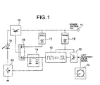
- an illuminance control circuit 10 is provided for generating a light adjustment pulse signal to perform the luminance control of a light emitting diode.
- a pulse amplitude stabilizing circuit 12 is a circuit for stabilizing an amplitude of the received light adjustment pulse signal.
- a pulse width adjusting circuit 13 is a circuit for changing a pulse time width of the pulse signal whose amplitude has been stabilized to a constant amplitude by the pulse amplitude stabilizing circuit 12 to a predetermined value.
- a power voltage Vcc is supplied to a power input terminal 11 from a power source unit (not shown) of a vehicle.
- a constant voltage driving circuit 15 functions as a constant voltage source for supplying a predetermined forward current to a light emitting diode 16 as a load by using the power voltage.
- a forward current interrupting circuit 20 is operative to interrupt (switch) the forward current flowing in the light emitting diode 16 as a load in response to the pulses generated from the pulse width adjusting circuit 13.
- the illuminance control circuit 10 a light adjustment pulse signal for performing the luminance control of the light emitting diode 16 is generated.
- the illuminance control circuit which is used for illuminating a console panel or the like of a vehicle is constructed by an extremely simple pulse generating circuit using an astable multivibrator.
- a duty factor of the light adjustment pulse signal which is generated from the circuit that is, a relative time width between the "1 level” and the "0 level” of the pulse or a frequency of the light adjustment pulse signal changes.
- the light adjustment pulse signal from the illuminance control circuit 10 is shaped into a pulse signal having a predetermined amplitude by the pulse amplitude stabilizing circuit 12.
- the pulse signal whose amplitude has been stabilized by the pulse amplitude stabilizing circuit 12 is supplied to the pulse width adjusting circuit 13.
- the circuit 13 is a circuit for adjusting the relative time width between the "1 level” and the "0 level” of the pulse signal.
- the adjustment of the time width is not uniformly determined but decided in dependence on characteristics of the light emitting diode 16 which is used in the circuit of the embodiment. That is, an adjustment is performed in a manner that the time width at the "1 level” in the pulse signal supplied to the circuit 13 is increased (or the time width at the "0 level” is reduced) in the case of a certain kind of light emitting diode. When using another kind of light emitting diode, the time width at the "1 level” in the pulse signal is reduced (or the time width at the "0 level” is increased).
- the DC voltage as an output from the smoothing circuit 14 is supplied to the control voltage input terminal of the constant voltage driving circuit 15 via the control voltage switching circuit 19.
- the constant voltage driving circuit 15 functions as a constant voltage source which is controlled by the output voltage from the smoothing circuit 14 and supplies the forward current according to the constant voltage to the light emitting diode 16 as a load.
- a process for smoothing the pulse signal as mentioned above is substantially equivalent to a process for integrating the pulse signal and obtaining its mean value, that is, a value of the DC voltage included in the pulse signal.
- the time width of the "1 level” in the pulse signal is constant, therefore, the level of the DC voltage obtained by smoothing the pulse signal raises as the frequency of the pulse signal increases.
- the value of the DC voltage obtained after the smoothing decreases as the frequency of the pulse signal decreases.
- the frequency of the pulse signal is constant, the larger the time width of the "1 level” in the pulse signal is than that of the "0 level", the higher the value of the DC voltage obtained in the case of smoothing the pulse signal is.
- the duty factor of the light adjustment pulse signal which is supplied to the circuit in Fig. 1, that is, the relative time width between the "1 level” and the "0 level” of the pulse or a frequency of the light adjustment pulse signal changes.
- the value of the DC output voltage from the smoothing circuit 14 changes and a luminance adjustment of the light emitting diode 16 is made.
- the relative time width between the "1 level” and the "0 level” of the pulse signal can be adjusted by the pulse width adjusting circuit 13 in accordance with the characteristics of the light emitting diode 16 as a load which is used.
- the motion of the illuminance adjustment knob therefore, can be adapted to the luminance change of the light emitting diode 16 which is actually used.
- the minimum voltage generating circuit 17 is provided and generates the minimum control voltage Vmin which is necessary when the constant voltage driving circuit 15 supplies the current IFmin.
- the switching position of the control voltage which is applied to the control voltage input of the constant voltage driving circuit 15 is not limited to a connecting position shown in Fig. 1.
- the control voltage switching circuit 19 can be also provided for an input unit of the smoothing circuit 14 as shown in Fig. 2.
- the voltage at a higher level is applied between the pulse signal voltage which is supplied from the pulse width adjusting circuit 13 and the output voltage from the minimum voltage generating circuit 17. That is, the voltage value Vmin from the minimum voltage generating circuit 17 is always applied to the control voltage input of the constant voltage driving circuit 15 and, in the voltage at the "1 level" of the pulse signal from the pulse width adjusting circuit 13, the voltage over Vmin is multiplexed to the voltage value Vmin.
- the output pulse signal from the pulse width adjusting circuit 13 is also supplied to the forward current interrupting circuit 20.
- the circuit 20 is a circuit for switching the forward current flowing in the light emitting diode 16 synchronously with the pulse signal. By directly switching the forward current by the pulse signal, the forward current also becomes a pulse signal synchronized with the pulse waveform.
- the mean value of the switched forward current therefore, differs in accordance with the frequency of the pulse signal or the relative time width between the "1 level” and the "0 level” in the pulse signal. That is, the luminance adjustment of the light emitting diode 16 can be also made by the switching process by the forward current interrupting circuit 20.
- the pulse signal which is supplied to the forward current interrupting circuit 20 is not limited to the output pulses from the pulse width adjusting circuit 13 but, for example, the light adjustment pulse signal from the illuminance control circuit 10 can be also directly used in accordance with the characteristics of the light emitting diode 16 which is used.
- mainly three functional circuits such as pulse width adjusting circuit 13, minimum voltage generating circuit 17, and forward current interrupting circuit 20 are provided.
- the luminance adjusting circuit of the invention it is not always necessary to provide all of those three functional circuits. That is, by combining at least two of those three functional circuits in accordance with the characteristics of the light emitting diode which is actually used as a load, a luminance change of the light emitting diode which is approximate to that of the conventional lamp can be obtained.
- FIG. 3 An example of a specific circuit construction regarding the embodiment is shown in Fig. 3.
- the pulse amplitude stabilizing circuit 12 comprises resistors R7 to R10 and transistors Q3 and Q4.
- the maximum voltage generating circuit 18 comprises a resistor R1 and a Zener diode ZD1.
- the resistor R1 and Zener diode ZD1 are serially connected and one end of the resistor R1 is connected to the power voltage Vcc.
- An anode of the Zener diode ZD1 is connected to the ground.
- Vmax as an output voltage of the maximum voltage generating circuit 18 is generated from a node of resistor R1 and Zener diode ZD1 (a cathode of the Zener diode ZD1).
- the minimum voltage generating circuit 17 comprises a resistor R2 and a Zener diode ZD2.
- the resistor R2 and Zener diode ZD2 are serially connected and one end of the resistor R2 is connected to the power voltage Vcc.
- An anode of the Zener diode ZD2 is connected to the ground.
- Vmin as an output voltage of the minimum voltage generating circuit 17 is generated from a node of resistor R2 and Zener diode ZD2 (a cathode of the Zener diode ZD2).
- the control voltage switching circuit 19 comprises diodes D1 and D2. Cathodes of those diodes are connected and a node thereof is used as an output of the control voltage switching circuit 19. An anode of the diode D1 is connected to an output of the minimum voltage generating circuit 17 (the cathode of the Zener diode ZD2). An anode of the diode D2 is connected to the collector of the transistor Q5 as an output of the pulse width adjusting circuit 13.
- the smoothing circuit 14 locating at the next stage of the control voltage switching circuit 19 comprises resistors R3 to R5 and capacitors C1 and C2.
- each of the resistors R3 and R5 is connected to an output of the control voltage switching circuit 19.
- the other end of the resistor R3 is connected to one end of each of the resistor R4 and capacitor C1.
- the other end of the resistor R4 is connected to one end of the capacitor C2 and used as an output of the smoothing circuit 14. All of the other ends of the resistor R5 and capacitors C1 and C2 are connected to the ground.
- the example of the specific circuit shown in Fig. 3 corresponds to the block diagram of Fig. 2 in which the positions of the smoothing circuit 14 and control voltage switching circuit 19 are opposite to those in the block diagram of Fig. 1.
- the control voltage which is formed from the pulse signal and generated from the illuminance control circuit can be also compared with the minimum control voltage Vmin after the pulse signal was smoothed.
- the smoothing circuit 14 shown in Fig. 3 is provided between the pulse width adjusting circuit 13 and control voltage switching circuit 19.
- the constant voltage driving circuit 15 comprises a resistor R6, transistors Q1 and Q2, and a diode D4.
- the output of the smoothing circuit 14 at the front stage is connected to a base of the transistor Q2.
- a collector of the transistor Q2 is connected to a base of the transistor Q1.
- An emitter of the transistor Q2 is connected to one end of the resistor R6 and a cathode of the diode D4, respectively.
- the other end of the resistor R6 is connected to the ground.
- An anode of the diode D4 is connected to a collector of the transistor Q1 as an output of the constant voltage driving circuit 15.
- the power voltage Vcc is supplied to an emitter of the transistor Q1.
- One end of the resistor R19 is connected to the output of the pulse width adjusting circuit 13 through a diode D3.
- the other end of the resistor R19 is connected to one end of the resistor R20 and a base of the transistor Q8.
- the other end of the resistor R20 and an emitter of the transistor Q8 are connected to the ground, respectively.
- a collector of the transistor Q8 is connected to the cathode of the light emitting diode LED 1 as a load.
- the output pulse from the pulse amplitude stabilizing circuit 12 is divided by the resistors R14 and R13 and applied to the base of the transistor Q7.
- the transistor Q7 is, therefore, turned on synchronously with the "1 level" of the input pulse signal. Since the input pulse signal is also applied to the serial circuit of the resistor R12 and capacitor C3, the capacitor C3 is charged to the voltage value Vmax corresponding to the amplitude of the "1 level" of the pulse signal through the resistor R12.
- the electric potential of the capacitor C3 decreases gradually.
- the connection between the capacitor C3 and the base of the transistor Q7 is disconnected.
- the base potential of the transistor Q7 is set to the "0 level" synchronously with the input pulse signal, and the transistor Q7 turns off.
- a circuit comprising the resistors R15 to R18 and transistors Q5 and Q6 in a range from the collector of the transistor Q7 to the post stage constructs a waveform shaping circuit.
- a pulse waveform whose amplitude is equal to the voltage Vmax as an output from the maximum voltage generating circuit is generated from the collector of the transistor Q5 in response to ON/OFF of the transistor Q7.
- the relative time width between the "1 level” and the "0 level” in the output pulse signal from the pulse amplitude stabilizing circuit 12 can be adjusted to a desired value.
- Figs. 4A to 4C show a voltage waveform at each point to which each of symbols ( a ) to ( c ) corresponds in the circuit diagram of Fig. 3. That is, Fig. 4A shows an input pulse waveform to the pulse width adjusting circuit 13. Fig. 4B shows a base potential of the transistor Q7 which changes slowly by the discharge of the capacitor C3. Fig. 4C shows an output pulse waveform from the pulse width adjusting circuit 13.
- the time width of the pulse which is extended can be set to a desired value by adjusting a time constant of a discharging circuit comprising the resistors R12 and R11 and capacitor C3 or a value of each constant in the pulse width adjusting circuit 13 such as a Zener voltage value of the Zener diode ZD3 or the like.
- the operation for shortening the time width of the "1 level" of the pulse signal in a manner opposite to that in the embodiment can be also easily realized by changing the construction and the connection of the charging/discharging circuit.
- the pulse width adjusting circuit 13 has been constructed by independent circuit parts, it can be also realized by an integrated circuit including a microcomputer which is driven by a software program.
- the kind of light emitting diode which is used as a load can be set by input means such as a dip switch.
- the pulse signal suitable for the luminance control of the light emitting diode which is actually used can be also easily generated without changing the circuit elements and circuit pattern.
- the output voltage Vmin from the minimum voltage generating circuit 17 is supplied to the anode of the diode D1.
- the output pulse signal from the pulse width adjusting circuit 13 is supplied to the anode of the diode D2. While the output pulse signal from the pulse width adjusting circuit 13 is at the "1 level”, therefore, the voltage value Vmax appears on the common cathode side of the control voltage switching circuit 19 due to the relation of Vmax > Vmin. While the pulse signal is at the "0 level", the voltage value Vmin appears on the common cathode side due to the relation of Vmin > 0. That is, in the case of the circuit shown in Fig. 3, the voltage waveform obtained by multiplexing the minimum control voltage Vmin to the output pulse signal from the pulse width adjusting circuit 13 appears as an output of the control voltage switching circuit 19.
- the smoothing circuit 14 constructs a ladder type smoothing circuit (integrating circuit) comprising the resistors R3 to R5 and capacitors C1 and C2.
- the voltage waveform obtained by smoothing (integrating) the input voltage that is, the DC voltage proportional to the mean value of the input voltage, therefore, appears as an output of the smoothing circuit 14.
- Figs. 5A to 5D show a voltage waveform at each point to which each of symbols ( c ) to ( f ) in the circuit diagram of Fig. 3 corresponds. That is, Fig. 5A shows an output pulse waveform from the pulse width adjusting circuit 13. Fig. 5B shows the output voltage Vmin from the minimum voltage generating circuit 17. Fig. 5C shows the output voltage of the control voltage switching circuit 19. Fig. 5D shows the output voltage of the smoothing circuit 14.
- the constant voltage driving circuit 15 is a constant voltage circuit comprising the transistors Q1 and Q2 and the like and generates a predetermined constant voltage from the power voltage Vcc. By the constant voltage, a predetermined forward current is supplied to the light emitting diodes 16 as a load serially connected to the constant voltage driving circuit 15.
- the constant voltage which is generated by the constant voltage driving circuit 15 is controlled in accordance with the control voltage which is applied to the base of the transistor Q2. That is, when the constant voltage which is applied to the base of the transistor Q2 is equal to the maximum control voltage Vmax, the constant voltage which enables the forward current IFmax to flow is generated by the constant voltage driving circuit 15. In the case of the minimum control voltage Vmin, the constant voltage which enables the forward current IFmin to flow is generated.
- the output pulse signal from the pulse width adjusting circuit 13 is also supplied to the forward current interrupting circuit 20 through the diode D3.
- the pulse signal is divided by the resistors R19 and R20 and applied to the base of the transistor Q8. That is, the transistor Q8 repeats the ON/OFF state synchronously with the input pulse signal.
- the light emitting diode 16 as a load is connected to the collector of the transistor Q8, the forward currents flowing in the light emitting diodes LED1 and LED2 are also interrupted by it.
- the pulse signal which is supplied to the forward current interrupting circuit 20 is not limited to the output from the pulse width adjusting circuit 13 but, for example, the light adjustment pulse signal from the illuminance control circuit 10 can be also directly used in accordance with the characteristics of the light emitting diode which is used.
- the luminance control circuit and the devices which are used can be reduced in size and the life span of the light source can be extended.
Landscapes
- Circuit Arrangement For Electric Light Sources In General (AREA)
- Led Devices (AREA)
- Control Of Indicators Other Than Cathode Ray Tubes (AREA)
Abstract
Description
Claims (5)
- A light emitting diode driving circuit comprising:a control pulse signal generator for generating a control pulse signal having a variable duty factor;a smoothing circuit for smoothing said control pulse signal to generate a control voltage;a driving circuit for generating a driving voltage according to said control voltage and supplying a forward current to said light emitting diode; anda switching circuit for interrupting the forward current of said light emitting diode in response to said control pulse signal.
- A circuit according to claim 1, wherein said control pulse signal generator comprises:a light adjustment pulse signal generating circuit for generating a light adjustment pulse signal of a duty factor according to a light adjustment amount; anda control pulse signal generating circuit for setting a pulse signal obtained by adjusting the duty factor of said light adjustment pulse signal to said control pulse signal.
- A circuit according to claim 2, wherein said switching circuit interrupts the forward current of said light emitting diode in response to said light adjustment pulse signal in place of said control pulse signal.
- A circuit according to any one of claims 1 to 3, further comprising:a minimum control voltage generating circuit for generating a predetermined minimum control voltage; anda control voltage switching circuit for setting said minimum control voltage to the control voltage of said driving circuit in place of said control voltage when said control voltage drops to a predetermined value or lower.
- A light emitting diode driving circuit comprising:a control pulse signal generator for generating a control pulse signal having a variable duty factor;a smoothing circuit for smoothing said control pulse signal to generate a control voltage;a driving circuit for generating a driving voltage according to said control voltage and supplying a forward current to said light emitting diode;a minimum control voltage generating circuit for generating a predetermined minimum control voltage; anda control voltage switching circuit for setting said minimum control voltage to the control voltage of said driving circuit in place of said control voltage when said control voltage drops to a predetermined value or lower,wherein said control pulse signal generator includesa light adjustment pulse signal generating circuit for generating a light adjustment pulse signal of a duty factor according to a light adjustment amount, anda control pulse adjusting circuit for adjusting change characteristics of the duty factor of said light adjustment pulse signal and generating said control pulse signal.
Applications Claiming Priority (2)
| Application Number | Priority Date | Filing Date | Title |
|---|---|---|---|
| JP2001027776A JP2002231470A (en) | 2001-02-05 | 2001-02-05 | Light emitting diode drive circuit |
| JP2001027776 | 2001-02-05 |
Publications (2)
| Publication Number | Publication Date |
|---|---|
| EP1229764A2 true EP1229764A2 (en) | 2002-08-07 |
| EP1229764A3 EP1229764A3 (en) | 2002-11-06 |
Family
ID=18892380
Family Applications (1)
| Application Number | Title | Priority Date | Filing Date |
|---|---|---|---|
| EP02001972A Ceased EP1229764A3 (en) | 2001-02-05 | 2002-02-04 | Light emitting diode driving circuit |
Country Status (3)
| Country | Link |
|---|---|
| US (1) | US6950079B2 (en) |
| EP (1) | EP1229764A3 (en) |
| JP (1) | JP2002231470A (en) |
Cited By (5)
| Publication number | Priority date | Publication date | Assignee | Title |
|---|---|---|---|---|
| WO2003009654A1 (en) * | 2001-07-19 | 2003-01-30 | Lumileds Lighting U.S., Llc | Led switching arrangement |
| WO2003009653A1 (en) * | 2001-07-19 | 2003-01-30 | Lumileds Lighting Us., Llc | Led switching arrangement |
| EP1689213A1 (en) * | 2005-02-02 | 2006-08-09 | Samsung Electronics Co., Ltd. | LED Driver circuit |
| WO2007148298A1 (en) * | 2006-06-22 | 2007-12-27 | Koninklijke Philips Electronics N.V. | Drive circuit for driving a load with pulsed current |
| CN107484299A (en) * | 2017-09-11 | 2017-12-15 | 四川蓝景光电技术有限责任公司 | LED degree of lightening toning temperature control circuit and its implementation method based on single channel PWM |
Families Citing this family (25)
| Publication number | Priority date | Publication date | Assignee | Title |
|---|---|---|---|---|
| US9153168B2 (en) * | 2002-07-09 | 2015-10-06 | Semiconductor Energy Laboratory Co., Ltd. | Method for deciding duty factor in driving light-emitting device and driving method using the duty factor |
| JP2005099349A (en) * | 2003-09-24 | 2005-04-14 | Pentax Corp | Lighting device |
| US6873203B1 (en) | 2003-10-20 | 2005-03-29 | Tyco Electronics Corporation | Integrated device providing current-regulated charge pump driver with capacitor-proportional current |
| KR100741963B1 (en) * | 2003-11-27 | 2007-07-23 | 삼성에스디아이 주식회사 | LCD and its driving method |
| JP4481083B2 (en) * | 2004-05-24 | 2010-06-16 | 三菱電機株式会社 | Light source drive voltage controller |
| KR100810516B1 (en) * | 2005-07-01 | 2008-03-10 | 삼성전자주식회사 | Load driving device and its load driving method |
| JP4267647B2 (en) * | 2006-08-10 | 2009-05-27 | 林化学工業株式会社 | Light emitting device |
| US8203260B2 (en) * | 2007-04-13 | 2012-06-19 | Intematix Corporation | Color temperature tunable white light source |
| US7703943B2 (en) * | 2007-05-07 | 2010-04-27 | Intematix Corporation | Color tunable light source |
| JP5144194B2 (en) * | 2007-09-25 | 2013-02-13 | パナソニック株式会社 | Lighting device and lighting apparatus |
| JP2009124027A (en) * | 2007-11-16 | 2009-06-04 | Sanyo Electric Co Ltd | Light emitting element driving circuit and mobile phone |
| JP5174529B2 (en) * | 2008-05-15 | 2013-04-03 | パナソニック株式会社 | LED dimming lighting device, vehicle lighting device, lighting fixture |
| US8836532B2 (en) * | 2009-07-16 | 2014-09-16 | Gentex Corporation | Notification appliance and method thereof |
| TW201111982A (en) * | 2009-09-29 | 2011-04-01 | Pegatron Corp | Displaying module, electronic apparatus and displaying method thereof |
| JP5405357B2 (en) * | 2010-03-04 | 2014-02-05 | 新電元工業株式会社 | Semiconductor lighting dimmer and integrated circuit |
| EP2410821B1 (en) | 2010-07-20 | 2014-01-08 | Panasonic Corporation | Lighting device of semiconductor light-emitting element and illumination fixture using the same |
| US8198832B2 (en) * | 2010-08-13 | 2012-06-12 | Linear Technology Corporation | Method and system for extending PWM dimming range in LED drivers |
| JP5691495B2 (en) * | 2010-12-24 | 2015-04-01 | 株式会社村田製作所 | LED driving power supply device and LED lighting device |
| TW201230866A (en) * | 2011-01-11 | 2012-07-16 | Top Energy Saving System Corp | Lighting device |
| FR2976150B1 (en) * | 2011-06-01 | 2013-06-14 | Thales Sa | DEVICE FOR CONTROLLING VERY LUMINOUS DYNAMIC LIGHT-EMITTING DIODES FOR DISPLAY SCREEN |
| JP2011187460A (en) * | 2011-07-01 | 2011-09-22 | Panasonic Electric Works Co Ltd | Lighting-up device for led dimming, vehicular lighting system, and lighting fixture |
| JP5853145B2 (en) * | 2011-07-26 | 2016-02-09 | パナソニックIpマネジメント株式会社 | LED lighting device and lighting apparatus using the same |
| TWI449287B (en) * | 2011-12-19 | 2014-08-11 | Lextar Electronics Corp | Over voltage protection circuit and driver circuit using the same |
| KR101365307B1 (en) * | 2012-04-20 | 2014-02-19 | 김영안 | Switching power supply circuit for LED lighting equipment |
| JP6769154B2 (en) * | 2016-07-27 | 2020-10-14 | 日本精機株式会社 | Head-up display |
Family Cites Families (23)
| Publication number | Priority date | Publication date | Assignee | Title |
|---|---|---|---|---|
| US3787752A (en) * | 1972-07-28 | 1974-01-22 | Us Navy | Intensity control for light-emitting diode display |
| JPS5636718A (en) | 1979-09-03 | 1981-04-10 | Matsushita Electric Works Ltd | Constant voltage circuit |
| JPS5837484B2 (en) * | 1979-09-25 | 1983-08-16 | 日産自動車株式会社 | Automotive electronic meter brightness control device |
| DE3339391A1 (en) | 1983-10-29 | 1985-05-09 | Robert Bosch Gmbh, 7000 Stuttgart | Electronically stabilised DC voltage power supply unit |
| US5068570A (en) * | 1989-01-26 | 1991-11-26 | Koito Manufacturing Co., Ltd. | Lamp lighting circuit with an overload protection capability |
| JPH02247688A (en) | 1989-03-20 | 1990-10-03 | Yokogawa Electric Corp | Luminance control circuit for led |
| CA2040626C (en) * | 1990-08-02 | 1995-05-23 | Shigeo Hayashi | Light emitting element drive circuit |
| JPH05158430A (en) * | 1991-12-03 | 1993-06-25 | Rohm Co Ltd | Display device |
| JPH05327450A (en) * | 1992-05-26 | 1993-12-10 | Alps Electric Co Ltd | Light emitting diode drive circuit |
| JPH0677534A (en) | 1992-08-25 | 1994-03-18 | Canon Inc | Recording device |
| US5978009A (en) * | 1992-10-14 | 1999-11-02 | Oki Electric Industry Co., Ltd. | Driving control circuit for an LED head |
| US5457450A (en) * | 1993-04-29 | 1995-10-10 | R & M Deese Inc. | LED traffic signal light with automatic low-line voltage compensating circuit |
| JP3294020B2 (en) * | 1994-10-31 | 2002-06-17 | エヌイーシー三菱電機ビジュアルシステムズ株式会社 | Power control circuit and power supply system |
| US5661645A (en) * | 1996-06-27 | 1997-08-26 | Hochstein; Peter A. | Power supply for light emitting diode array |
| JPH10135520A (en) | 1996-10-30 | 1998-05-22 | N O Ke G & G Opt Electron Kk | Light emitting rivet, its control system and use method of light emitting rivet |
| US5783909A (en) * | 1997-01-10 | 1998-07-21 | Relume Corporation | Maintaining LED luminous intensity |
| JPH10243171A (en) * | 1997-02-25 | 1998-09-11 | Brother Ind Ltd | Image reading device |
| US5850126A (en) * | 1997-04-11 | 1998-12-15 | Kanbar; Maurice S. | Screw-in led lamp |
| JPH11109919A (en) | 1997-09-30 | 1999-04-23 | Toyota Motor Corp | PWM driving method and circuit |
| US6236331B1 (en) * | 1998-02-20 | 2001-05-22 | Newled Technologies Inc. | LED traffic light intensity controller |
| US6111739A (en) * | 1999-08-11 | 2000-08-29 | Leotek Electronics Corporation | LED power supply with temperature compensation |
| DE10013208A1 (en) | 2000-03-17 | 2001-09-20 | Tridonic Bauelemente Gmbh Dorn | Control of light-emitting diodes (leds) |
| DE10025821A1 (en) * | 2000-05-25 | 2002-07-25 | Sickinger Monika | LED light source |
-
2001
- 2001-02-05 JP JP2001027776A patent/JP2002231470A/en active Pending
-
2002
- 2002-02-01 US US10/060,398 patent/US6950079B2/en not_active Expired - Fee Related
- 2002-02-04 EP EP02001972A patent/EP1229764A3/en not_active Ceased
Cited By (8)
| Publication number | Priority date | Publication date | Assignee | Title |
|---|---|---|---|---|
| WO2003009654A1 (en) * | 2001-07-19 | 2003-01-30 | Lumileds Lighting U.S., Llc | Led switching arrangement |
| WO2003009653A1 (en) * | 2001-07-19 | 2003-01-30 | Lumileds Lighting Us., Llc | Led switching arrangement |
| EP1689213A1 (en) * | 2005-02-02 | 2006-08-09 | Samsung Electronics Co., Ltd. | LED Driver circuit |
| US7295176B2 (en) | 2005-02-02 | 2007-11-13 | Samsung Electronics Co., Ltd. | LED driver with constant current offset unit |
| WO2007148298A1 (en) * | 2006-06-22 | 2007-12-27 | Koninklijke Philips Electronics N.V. | Drive circuit for driving a load with pulsed current |
| US8063581B2 (en) | 2006-06-22 | 2011-11-22 | Koninklijke Philips Electronics N.V. | Drive circuit for driving a load with pulsed current |
| CN107484299A (en) * | 2017-09-11 | 2017-12-15 | 四川蓝景光电技术有限责任公司 | LED degree of lightening toning temperature control circuit and its implementation method based on single channel PWM |
| CN107484299B (en) * | 2017-09-11 | 2024-04-19 | 四川蓝景光电技术有限责任公司 | LED lamp brightness and color temperature adjusting control circuit based on one-way PWM and implementation method thereof |
Also Published As
| Publication number | Publication date |
|---|---|
| US6950079B2 (en) | 2005-09-27 |
| EP1229764A3 (en) | 2002-11-06 |
| JP2002231470A (en) | 2002-08-16 |
| US20020105487A1 (en) | 2002-08-08 |
Similar Documents
| Publication | Publication Date | Title |
|---|---|---|
| EP1229764A2 (en) | Light emitting diode driving circuit | |
| US7463070B2 (en) | Switching device for driving LED array by pulse-shaped current modulation | |
| US8248001B2 (en) | LED control circuit and method, and insect resistive LED lamp | |
| US6867557B2 (en) | Lighting circuit | |
| RU2416179C2 (en) | Apparatus for supplying luminous elements with energy and method of powering luminous elements | |
| US7750579B2 (en) | LED driving device with variable light intensity | |
| US6127786A (en) | Ballast having a lamp end of life circuit | |
| CN102833909B (en) | Light-emitting device and the lighting apparatus with light-emitting device | |
| KR20090093949A (en) | A switched light element array and method of operation | |
| WO2006043636A1 (en) | Power supply for semiconductor light emitting element and lighting equipment | |
| JP3939517B2 (en) | Dimming control circuit | |
| US7755304B2 (en) | Three-way dimming ballast circuit | |
| JP2012146646A (en) | Led light-emitting device, terminal number converter and lighting apparatus | |
| CN108633124B (en) | Dimmable LED lamp, operation method thereof and lamp driver for dimmable LED lamp | |
| KR100953009B1 (en) | Remote control transmitter | |
| KR102052852B1 (en) | High power factor three step dimming converter for led lighting apparatus | |
| CN215187479U (en) | Light modulation circuit | |
| JP3680561B2 (en) | Inverter device | |
| CN113411932A (en) | Constant-brightness LED circuit and electronic equipment | |
| CN108668400B (en) | LED lamp | |
| JP2004134580A (en) | Driver circuit for light emitting diode | |
| KR102460625B1 (en) | Device for flicker-free and lighting apparatus including the same | |
| CN221043270U (en) | Color mixing LED lighting system and dimming control circuit thereof | |
| CN111385485A (en) | Image acquisition equipment and electronic device | |
| JP2004328949A (en) | Switching constant current power supply |
Legal Events
| Date | Code | Title | Description |
|---|---|---|---|
| PUAI | Public reference made under article 153(3) epc to a published international application that has entered the european phase |
Free format text: ORIGINAL CODE: 0009012 |
|
| AK | Designated contracting states |
Kind code of ref document: A2 Designated state(s): AT BE CH CY DE DK ES FI FR GB GR IE IT LI LU MC NL PT SE TR |
|
| AX | Request for extension of the european patent |
Free format text: AL;LT;LV;MK;RO;SI |
|
| PUAL | Search report despatched |
Free format text: ORIGINAL CODE: 0009013 |
|
| AK | Designated contracting states |
Kind code of ref document: A3 Designated state(s): AT BE CH CY DE DK ES FI FR GB GR IE IT LI LU MC NL PT SE TR |
|
| AX | Request for extension of the european patent |
Free format text: AL;LT;LV;MK;RO;SI |
|
| 17P | Request for examination filed |
Effective date: 20021115 |
|
| AKX | Designation fees paid |
Designated state(s): DE FR GB |
|
| 17Q | First examination report despatched |
Effective date: 20040401 |
|
| APBN | Date of receipt of notice of appeal recorded |
Free format text: ORIGINAL CODE: EPIDOSNNOA2E |
|
| APBR | Date of receipt of statement of grounds of appeal recorded |
Free format text: ORIGINAL CODE: EPIDOSNNOA3E |
|
| APAF | Appeal reference modified |
Free format text: ORIGINAL CODE: EPIDOSCREFNE |
|
| APBT | Appeal procedure closed |
Free format text: ORIGINAL CODE: EPIDOSNNOA9E |
|
| STAA | Information on the status of an ep patent application or granted ep patent |
Free format text: STATUS: THE APPLICATION HAS BEEN WITHDRAWN |
|
| 18W | Application withdrawn |
Effective date: 20080423 |
|
| 18R | Application refused |
Effective date: 20080423 |