EP1229618A2 - Discharge gap apparatus - Google Patents
Discharge gap apparatus Download PDFInfo
- Publication number
- EP1229618A2 EP1229618A2 EP01121856A EP01121856A EP1229618A2 EP 1229618 A2 EP1229618 A2 EP 1229618A2 EP 01121856 A EP01121856 A EP 01121856A EP 01121856 A EP01121856 A EP 01121856A EP 1229618 A2 EP1229618 A2 EP 1229618A2
- Authority
- EP
- European Patent Office
- Prior art keywords
- discharge
- gap
- terminal
- sections
- primary
- Prior art date
- Legal status (The legal status is an assumption and is not a legal conclusion. Google has not performed a legal analysis and makes no representation as to the accuracy of the status listed.)
- Granted
Links
Images


Classifications
-
- H—ELECTRICITY
- H05—ELECTRIC TECHNIQUES NOT OTHERWISE PROVIDED FOR
- H05K—PRINTED CIRCUITS; CASINGS OR CONSTRUCTIONAL DETAILS OF ELECTRIC APPARATUS; MANUFACTURE OF ASSEMBLAGES OF ELECTRICAL COMPONENTS
- H05K1/00—Printed circuits
- H05K1/02—Details
- H05K1/0213—Electrical arrangements not otherwise provided for
- H05K1/0254—High voltage adaptations; Electrical insulation details; Overvoltage or electrostatic discharge protection ; Arrangements for regulating voltages or for using plural voltages
- H05K1/0257—Overvoltage protection
- H05K1/026—Spark gaps
-
- H—ELECTRICITY
- H01—ELECTRIC ELEMENTS
- H01T—SPARK GAPS; OVERVOLTAGE ARRESTERS USING SPARK GAPS; SPARKING PLUGS; CORONA DEVICES; GENERATING IONS TO BE INTRODUCED INTO NON-ENCLOSED GASES
- H01T4/00—Overvoltage arresters using spark gaps
- H01T4/08—Overvoltage arresters using spark gaps structurally associated with protected apparatus
-
- H—ELECTRICITY
- H05—ELECTRIC TECHNIQUES NOT OTHERWISE PROVIDED FOR
- H05K—PRINTED CIRCUITS; CASINGS OR CONSTRUCTIONAL DETAILS OF ELECTRIC APPARATUS; MANUFACTURE OF ASSEMBLAGES OF ELECTRICAL COMPONENTS
- H05K2201/00—Indexing scheme relating to printed circuits covered by H05K1/00
- H05K2201/10—Details of components or other objects attached to or integrated in a printed circuit board
- H05K2201/10007—Types of components
- H05K2201/10015—Non-printed capacitor
Definitions
- This invention relates to a discharge gap apparatus favorably adopted in a power receiving section for receiving power particularly from a commercial AC power supply in a printed circuit board used in TV sets, videotape recorders, and electronic equipment such as communications equipment.
- a power receiving section includes a lightning-stroke protection circuit.
- This circuit aims at releasing a lightning voltage guided to an external antenna and supplying the resultant lightning voltage toward an external commercial AC power supply. This technique is disclosed in Jpn. Pat. Appln. KOKAI Publication No. 2000-69666.
- the lightning-stroke protection circuit includes a discharge gap circuit, and a discharge gap is discharged when lightning strikes. Paying attention to the discharge gap circuit, it is preferable to reduce the discharge gap and drop a lightning surge discharge start voltage in order to smoothly discharge the discharge gap when lightning strikes.
- Individual countries set their respective standards for safety for the discharge gap circuit. In other words, a distance between the primary and secondary parts (conductors) of the circuit is defined. Because of the standards for safety, the gap cannot be decreased carelessly. The distance between the primary and secondary conductors, which conforms to the standards for safety, contradicts with a reduction in the discharge gap to lower the lightning surge discharge start voltage.
- a discharge gap apparatus comprises a discharge gap section including first and second conductive patterns arranged on an insulating substrate at regular intervals and a third conductive pattern arranged thereon close to the first and second conductive patterns, a first gap being formed between the first and third conductive patterns, and a second gap being formed between the second and third conductive patterns; connecting terminal sections provided in the second and third conductive patterns, respectively and located away from the second gap, an interval between the connecting terminal sections being greater than the second gap; and a capacitor connected between the connecting terminal sections.
- a discharge gap apparatus comprises a primary terminal having a first discharge section; a secondary terminal having a second discharge section and arranged at a given distance from the primary terminal; a third terminal provided close to the first discharge section and the second discharge section and having third and fourth discharge sections opposed to the first and second discharge sections, respectively, a first gap being formed between the first and third discharge sections, and a second gap being formed between the second and fourth discharge sections; connecting terminal sections provided in the secondary and third terminals, respectively and located away from the second gap, an interval between the connecting terminal sections being greater than the second gap; and a capacitor connected between the connecting terminal sections.
- the capacitor fulfills a function of inducing discharge.
- the discharge start voltage can thus be lowered to obtain smooth discharge.
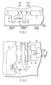
- FIG. 1 illustrates a basic structure of a discharge gap apparatus according to a first embodiment of the present invention.
- reference numeral 100 indicates a printed wiring board.
- Primary and secondary terminals 11 and 22 are printed by patterning on the printed wiring board 100.
- the primary terminal 11 includes a primary discharge section 1 for discharge, while the secondary terminal 22 includes a secondary discharge section 2 for discharge.
- a floating-point terminal 33 is printed by patterning between the primary and secondary terminals 11 and 22.
- This terminal 33 has first and second floating-point discharge sections 31 and 32 on a line connecting the primary and secondary discharge sections 1 and 2. These sections 31 and 32 are integrated as one component.
- a capacitor 44 for connecting the floating-point terminal 33 and the secondary terminal 22 is provided away from the line connecting the sections 1 and 2.
- the capacitor 44 is located in a space having a distance L3 (e.g., 7.5 mm) that is greater than the shortest distance between the terminals 22 and 33.
- the terminals 22 and 33 have their extended terminal portions 24 and 34, respectively.
- the foregoing discharge gap apparatus has a two-stage discharge gap structure.
- a first discharge gap is formed between the primary discharge section 1 and the first floating-point discharge section 31 and a second discharge gap is formed between the second floating-point discharge sections 32 and the secondary discharge section 2.
- the capacitor 44 (which satisfies a standard for withstand voltages) is connected between the secondary terminal 22 and the floating-point terminal 33 to lower a lightning surge discharge start voltage.
- the total of the first discharge gap L1 (e.g., 3.5 mm) and the second discharge gap L2 (e.g., 3 mm) is 6 mm or more. This value satisfies standards for safety (IEC, UL, CSA, and the Electrical Appliance and Material Control Law) that define a gap between the primary and secondary conductors.
- standards for safety IEC, UL, CSA, and the Electrical Appliance and Material Control Law
- a given gap should be set between the primary and secondary terminals.
- the capacitor 44 is connected between the secondary terminal 22 and the floating-point terminal 33 which are separated from each other with a gap of 3 mm therebetween.
- the capacitor 44 conforms to the standards for safety and satisfies an insulating function under the standards.
- a line bypass capacitor (popularly called a Y capacitor) is adopted to satisfy the standards for safety in each country.
- the capacitor Under the IEC standard, the capacitor is classified as IEC 384-14, second edition, class II. Under the UL and CSA standards, it is classified as IEC 348-14, second edition, class I (or class II). Under the Electrical Appliance and Material Control Law, it is classified as IEC 348-14, second edition, class I or class II. The design standard is therefore satisfied even though the capacitor 44 is provided.
- the capacitor 44 Since the capacitor 44 is connected between the floating-point terminal 33 and the secondary terminal 22, these terminals are insulated from each other at the same potential in the early stage. If a lightning voltage is guided, discharge (a short circuit) is caused between the primary discharge section 1 of the primary terminal 11 and the first floating-point discharge section 31 of the floating-point terminal 33 and then between the second floating-point discharge section 32 of the floating-point terminal 33 and the secondary discharge section 2 of the secondary terminal 22. Consequently, the primary and secondary terminals are discharged.
- the capacitor 44 allows a lightning surge discharge start voltage to drop when lightning strikes.
- the capacitor 44 Since the lightning voltage has a high frequency, the capacitor 44 is considered to be short-circuited when lightning strikes. This situation is equal to the application of a lightning voltage only between the primary terminal 11 and the floating-point terminal 33. The narrower the gap, the lower the discharge start voltage. Thus, the discharge start voltage in the above apparatus is lower than that in an apparatus having no capacitors.
- Discharge means that an insulator is punctured and short-circuited.
- the short-circuited portion is located between the primary discharge section 1 and the first floating-point discharge section 31 and between the second floating-point discharge section 32 and the secondary discharge section 2.
- Discharge current flows through the short-circuited portion and not through the capacitor 44. This phenomenon depends upon the connecting position of the capacitor 44.
- the capacitor 44 is located at a distance from the line connecting the primary and secondary discharge sections 1 and 2, and connects the secondary discharge section 2 and the second floating-point discharge section 32 in a space whose width L3 is greater than the shortest distance L2.
- FIG. 2 illustrates a charge gap apparatus according to a second embodiment of the present invention.
- the constituting elements of the apparatus which correspond to those of the first embodiment, will be described with the same reference numerals assigned thereto.
- reference numeral 100 indicates a printed wiring board on which terminals (described below) are printed by patterning.
- Reference numeral 51 denotes a plug connected to a commercial AC power supply.
- One line (A pole) of the plug is connected to an A-pole primary terminal 11a and the other line (B pole) thereof is connected to a B-pole primary terminal 11b.
- the A-pole primary terminal 11a includes a primary discharge section 1a for discharge, while a secondary terminal 22 includes a secondary discharge section 2a for discharge.
- the B-pole primary terminal 11b includes a primary discharge section 1b for discharge, while the secondary terminal 22 includes a secondary discharge section 2b for discharge.
- the primary terminals 11a and 11b are arranged in parallel with and independently of each other.
- a floating-point terminal 33 is printed by patterning between the primary terminals 11a and 11b and the secondary terminal 22.
- the terminal 33 includes a first floating-point discharge section 31a and a second floating-point discharge section 32a on a line connecting the primary and secondary discharge sections 1a and 2a.
- the discharge sections 31a and 32a are integrated as one component.
- the terminal 33 also includes a first floating-point discharge section 31b and a second floating-point discharge section 32b on a line connecting the primary and secondary discharge sections 1b and 2b.
- the discharge sections 31b and 32b are integrated as one component.
- a capacitor 44 for connecting the secondary terminal 22 and the floating-point terminal 33 is provided at a distance from the primary discharge sections 1a and 1b and the secondary discharge sections 2a and 2b.
- the capacitor 44 is located in a space having a distance L3 (e.g., 7.5 mm) that is greater than the shortest distance between the terminals 22 and 33.
- L3 e.g., 7.5 mm
- the secondary terminal 22 has a notch 253 such that a portion 251 of the terminal 22, which is connected to the capacitor 44, separates from an edge 252 of the secondary terminal 22 through which a discharge current is easy to flow.
- the notch 253 is effective in preventing a discharge current from flowing into the capacitor 44 when lightning strikes.
- the board 100 has a slit-like opening 55.
- the discharge sections 1a, 1b, 31a, 32a, 31b, 32b, 2a and 2b each have a pair of pointed projections toward a discharge gap.
- the second embodiment fulfills the same function as that of the first embodiment described above.
- FIG. 3 depicts a charge gap apparatus according to a third embodiment of the present invention.
- the constituting elements of the apparatus which correspond to those of the second embodiment, will be described with the same reference numerals assigned thereto.
- an A-pole line of a plug 51 is connected to a primary terminal 11a via a printed pattern 61, while a B-pole line thereof is connected to another primary terminal 11b via a printed pattern 62, a fuse 63, a printed pattern 64, and a jumper wire 65.
- the other elements are almost the same as those of the apparatus shown in FIG. 2.
- Each of discharge sections 1a, 1b, 31a, 32a, 31b, 32b, 2a and 2b are thickened because solder is attached thereto. Thus, the discharge sections can maintain their durability even though they are cut by discharge. While the thickness of a printed wiring pattern is 35 microns, that of the thickest solder portion of each discharge section is about 0.5 mm.
- FIG. 4 is a circuit diagram simply showing a power receiving section to which the present invention is applied.
- the constituents corresponding to those of the above embodiments are denoted by the same reference numerals.
- A-pole of a power line is connected to a printed pattern 61 and a B-pole thereof is connected to another printed pattern 62.
- a capacitor 71 is an insulating capacitor connected between A-pole and B-pole lines.
- Diodes 72 and 73 are connected in series between these lines as protection circuits.
- Numeral 74 indicates a transformer for transforming an input voltage. It is discharge sections 75 and 76 that the present invention is applied to.
- the discharge gap apparatus is provided on a printed wiring board having a power receiving section and a secondary terminal integrally as one component.
- the elements as shown in FIGS. 1, 2 and 3 can be constituted as a single component.
- distance W between the primary and secondary terminals 11 and 22 each constituting a discharge section under the standards of the Electrical Appliance and Material Control Law, UL, CSA and IEC-65.
- the distance W is 2.0 mm or longer under the standard of the Electrical Appliance and Material Control Law, 3.2 mm or longer under the UL standard, 3.0 mm or longer under the CSA standard, and 6.0 mm or longer under the IEC-65 standard.
- Providing a floating-point terminal 33 as in the present invention, its position has to be determined so as to satisfy the distance W. In other words, distance W1 should be set between the discharge sections 1 and 31 and so should be distance W2 between the discharge sections 32 and 2.
- distance W1 is 1.0 mm to 2.8 mm (preferably 2.0 mm) and distance W2 is 1.0 mm to 2.1 mm (preferably 1.5 mm).
- the standard of the Electrical Appliance and Material Control Law is therefore satisfied when distance W is 2 mm or longer.
- distance W1 is 1.0 mm to 3.5 mm (preferably 2.0 mm) and distance W2 is 1.0 mm to 2.0 mm (preferably 1.5 mm).
- the UL standard is therefore satisfied when distance W is 3.2 mm to 4.0 mm.
- distance W1 is 1.0 mm to 3.3 mm (preferably 2.0 mm) and distance W2 is 1.0 mm to 2.0 mm (preferably 1.5 mm). The CSA standard is therefore satisfied when distance W is 3.0 mm to 4.0 mm.
- distance W1 is 3.0 mm to 4.5 mm (preferably 3.5 mm) and distance W2 is 2.0 mm to 4.5 mm (preferably 3.0 mm). The IEC-65 standard is therefore satisfied when distance W is 6.0 mm to 8.0 mm.
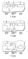
- the pattern of the discharge gap apparatus of the present invention is not limited to those shown in FIGS. 1 to 3.
- the apparatus can be constituted in the patterns as illustrated in FIGS. 5A to 5E.
- the primary terminal 11, secondary terminal 22 and floating-point terminal 33 are arranged linearly.
- Terminal portions 24 and 34 are located at a distance from a gap formed between discharge sections 2 and 32. The interval between the terminal portions 24 and 34 is greater than the gap.
- the secondary terminal 22 and the floating-point terminal 33 are arranged in parallel with a given gap therebetween.
- the terminal portions 24 and 34 are located at a distance from a gap formed between the discharge sections 2 and 32. The interval between the terminal portions 24 and 34 is greater than the gap.
- a gap between the discharge sections 1 and 31 and a gap between the discharge sections 2 and 32 are displaced up and down from each other.
- the terminal portions 24 and 34 are located at a distance from the gap formed between the discharge sections 2 and 32. The interval between the terminal portions 24 and 34 is greater than the gap.
- a terminal portion 14 is provided at the primary terminal 11 and a capacitor 44 is connected between the terminal portion 14 and the terminal portion 34 of the floating-point terminal 33.
- the terminal portions 14 and 34 are located at a distance from a gap formed between the discharge sections 1 and 31. The interval between the terminal portions 14 and 34 is greater than the gap.
- the primary and secondary terminals 11 and 22 are arranged up and down, and a floating-point terminal 33 is provided opposite to the discharge sections 1 and 2.
- Discharge sections 31 and 32 are formed at the terminal 33 so as to face the discharge sections 1 and 2.
- the terminal portions 24 and 34 are located a distance from a gap formed between the discharge sections 2 and 32, and the interval between the terminal portions 24 and 34 is greater than the gap.
Landscapes
- Engineering & Computer Science (AREA)
- Microelectronics & Electronic Packaging (AREA)
- Emergency Protection Circuit Devices (AREA)
- Structure Of Printed Boards (AREA)
- Coupling Device And Connection With Printed Circuit (AREA)
Abstract
Description
Claims (24)
- A discharge gap apparatus characterized by comprising:a discharge gap section including first and second conductive patterns (11, 22) arranged on an insulating substrate at regular intervals and a third conductive pattern (33) arranged thereon close to the first and second conductive patterns (11, 22), a first gap (L1) being formed between the first and third conductive patterns, and a second gap (L2) being formed between the second and third conductive patterns;connecting terminal sections (24, 34) provided in the second and third conductive patterns, respectively and located away from the second gap (L2), an interval between the connecting terminal sections being greater than the second gap; anda capacitor (44) connected between the connecting terminal sections.
- The discharge gap apparatus according to claim 1, characterized in that a total (L1 + L2) of the first gap and the second gap is set to satisfy an insulation standard.
- The discharge gap apparatus according to claim 1, characterized in that the first conductive pattern (11) is connected to a commercial AC power supply constituting a primary circuit and the second conductive pattern (22) is connected to a connection point of a secondary circuit.
- The discharge gap apparatus according to claim 1, characterized in that the third conductive pattern (33) is provided between the first conductive pattern (11) and the second conductive pattern (22).
- The discharge gap apparatus according to claim 4, characterized in that the first gap (L1) and the second gap (L2) are arranged linearly.
- A discharge gap apparatus characterized by comprising:a primary terminal (11) having a first discharge section (1);a secondary terminal (22) having a second discharge section (2) and arranged at a given distance from the primary terminal;a third terminal (33) provided close to the first discharge section (1) and the second discharge section (2) and having third and fourth discharge sections (31, 32) opposed to the first and second discharge sections (1, 2), respectively, a first gap (L1) being formed between the first and third discharge sections, and a second gap (L2) being formed between the second and fourth discharge sections;connecting terminal sections (24, 34) provided in the secondary and third terminals, respectively and located away from the second gap (L2), an interval between the connecting terminal sections being greater than the second gap; anda capacitor (44) connected between the connecting terminal sections.
- The discharge gap apparatus according to claim 6, characterized in that the primary terminal (11), the secondary terminal (22) and the third terminal (33) are printed on a printed wiring board (100).
- The discharge gap apparatus according to claim 6, characterized in that a total (L1 + L2) of the first gap (L1) and the second gap (L2) is set to satisfy an insulation standard.
- The discharge gap apparatus according to claim 6, characterized in that the primary terminal (11) is connected to a commercial AC power supply constituting a primary circuit and the secondary terminal (22) is connected to a connection point of a secondary circuit.
- The discharge gap apparatus according to claim 6, characterized in that solder is attached to the first, second, third and fourth discharge sections.
- The discharge gap apparatus according to claim 6, characterized in that the discharge sections (1, 31; 2, 32) opposed to each other each have a plurality of pointed projections.
- The discharge gap apparatus according to claim 6, characterized in that a slit (55) is formed in a lower part of at least one of the first and second gaps.
- The discharge gap apparatus according to claim 6, characterized in that when the first gap is W1 and the second gap is W2, W1 = 3.0 mm to 4.5 mm (preferably 3.5 mm), W2 = 2.0 mm to 4.5 mm (preferably 3.0 mm), and W1 + W2 = 6.0 mm to 8.0 mm.
- The discharge gap apparatus according to claim 6, characterized in that when the first gap is W1 and the second gap is W2, W1 = 1.0 mm to 2.8 mm (preferably 2.0 mm), W2 = 1.0 mm to 2.1 mm (preferably 1.5 mm), and W1 + W2 = 2.0 mm or more.
- The discharge gap apparatus according to claim 6, characterized in that when the first gap is W1 and the second gap is W2, W1 = 1.0 mm to 3.5 mm (preferably 2.0 mm), W2 = 1.0 mm to 2.0 mm (preferably 1.5 mm), and W1 + W2 = 3.2 mm to 4.0 mm.
- The discharge gap apparatus according to claim 6, characterized in that when the first gap is W1 and the second gap is W2, W1 = 1.0 mm to 3.3 mm (preferably 2.0 mm), W2 = 1.0 mm to 2.0 mm (preferably 1.5 mm), and W1 + W2 = 3.0 mm to 4.0 mm.
- The discharge gap apparatus according to claim 6, characterized in that the primary terminal (11) includes a pair of terminals (11a, 11b) each having a primary discharge section, the secondary terminal (22) includes a pair of second discharge sections (2a, 2b), and the third terminal (33) includes pairs of third and fourth discharge sections (31a, 31b; 32a, 32b).
- The discharge gap apparatus according to claim 17, characterized in that an interval between the terminals of the primary terminal is set at 3 mm or more.
- A discharge gap apparatus characterized by comprising:a primary terminal (11) having a first discharge section;a secondary terminal (22) arranged at a given distance from the primary terminal and having a second discharge section opposed to the first discharge section;a floating-point terminal (33) arranged between the first and second discharge sections and having third and fourth discharge sections opposed to the first and second discharge sections, respectively, a first gap (L1) being formed between the first and third discharge sections and a second gap (L2) being formed between the second and fourth discharge sections;connecting terminals (24, 34) provided in the secondary terminal and the floating-point terminal, respectively and located away from the second gap (L2), an interval between the connecting terminals being greater than the second gap; anda capacitor (44) connected between the connecting terminals.
- The discharge gap apparatus according to claim 19, characterized in that the first gap and the second gap are arranged linearly.
- A discharge gap apparatus formed on a printed wiring board, characterized by comprising:a first primary pattern (11a) including a first discharge section (1a) having a plurality of pointed projections;a second primary pattern (11b) including a second discharge section (1b) having a plurality of pointed projections and formed at a given distance from the first primary pattern (11a);a secondary pattern (22) formed at a distance from the first and second primary patterns (11a, 11b) and including a pair of third discharge sections (2a, 2b) opposed to the first and second discharge sections;a floating-point pattern (33) arranged between the primary patterns (11a, 11b) and the secondary pattern (22), and including a pair of fourth discharge sections (31a, 31b) opposed to the first and second discharge sections (1a, 1b), respectively and a pair of fifth discharge sections (32a, 32b) opposed to the third discharge sections (2a, 2b), respectively, a first gap being formed between the first and second discharge sections and the fourth discharge sections, and a second gap being formed between the third discharge sections and the fifth discharge sections;connecting terminals (24, 34) provided in the secondary pattern (22) and the floating-point pattern (33), respectively and located away from the second gap, an interval between the connecting terminals being greater than the second gap; anda discharge-inducing capacitor (44) connected between the connecting terminals (24, 34).
- The discharge gap apparatus according to claim 21, characterized in that a slit (55) is formed in the board where at least one of the first gap and the second gap is located.
- The discharge gap apparatus according to claim 21, characterized in that a total of the first gap and the second gap is set to satisfy an insulation standard.
- The discharge gap apparatus according to claim 21, characterized in that solder is attached to the first, second, third, fourth and fifth discharge sections.
Applications Claiming Priority (2)
| Application Number | Priority Date | Filing Date | Title |
|---|---|---|---|
| JP2001023968A JP3626414B2 (en) | 2001-01-31 | 2001-01-31 | Discharge gap device |
| JP2001023968 | 2001-01-31 |
Publications (3)
| Publication Number | Publication Date |
|---|---|
| EP1229618A2 true EP1229618A2 (en) | 2002-08-07 |
| EP1229618A3 EP1229618A3 (en) | 2004-05-12 |
| EP1229618B1 EP1229618B1 (en) | 2008-02-13 |
Family
ID=18889175
Family Applications (1)
| Application Number | Title | Priority Date | Filing Date |
|---|---|---|---|
| EP20010121856 Expired - Lifetime EP1229618B1 (en) | 2001-01-31 | 2001-09-11 | Discharge gap apparatus |
Country Status (5)
| Country | Link |
|---|---|
| EP (1) | EP1229618B1 (en) |
| JP (1) | JP3626414B2 (en) |
| CN (1) | CN1316701C (en) |
| DE (1) | DE60132759T2 (en) |
| SG (1) | SG90783A1 (en) |
Cited By (5)
| Publication number | Priority date | Publication date | Assignee | Title |
|---|---|---|---|---|
| EP1612898A1 (en) * | 2004-06-30 | 2006-01-04 | Research In Motion Limited | Spark gap apparatus and method for electrostatic discharge protection |
| EP1612897A1 (en) * | 2004-06-30 | 2006-01-04 | Research In Motion Limited | Spark gap apparatus and method for electrostatic discharge protection |
| US7161784B2 (en) | 2004-06-30 | 2007-01-09 | Research In Motion Limited | Spark gap apparatus and method for electrostatic discharge protection |
| US7508644B2 (en) | 2004-06-30 | 2009-03-24 | Research In Motion Limited | Spark gap apparatus and method for electrostatic discharge protection |
| EP2051339A1 (en) * | 2007-08-21 | 2009-04-22 | Giga-Byte Technology Co., Ltd. | Connector and printed circuit board |
Families Citing this family (5)
| Publication number | Priority date | Publication date | Assignee | Title |
|---|---|---|---|---|
| KR100700692B1 (en) | 2004-10-04 | 2007-03-27 | 주식회사 대우일렉트로닉스 | Patterning method of printed circuit board |
| JP5289697B2 (en) * | 2006-10-03 | 2013-09-11 | 株式会社キッツ | Switching power supply and electric valve actuator |
| WO2008090842A1 (en) * | 2007-01-24 | 2008-07-31 | Daikin Industries, Ltd. | Terminal table |
| JP2010021209A (en) * | 2008-07-08 | 2010-01-28 | Mitsumi Electric Co Ltd | Discharge gap pattern and power source device |
| JP5304997B2 (en) * | 2008-10-09 | 2013-10-02 | 三菱マテリアル株式会社 | surge absorber |
Family Cites Families (6)
| Publication number | Priority date | Publication date | Assignee | Title |
|---|---|---|---|---|
| JPH0422086A (en) * | 1990-05-17 | 1992-01-27 | Cosel Usa Inc | Protection circuit against surge voltage |
| SE9701195L (en) * | 1997-04-02 | 1998-10-03 | Ericsson Telefon Ab L M | Device for protection against electrostatic discharge in electrical appliances |
| TW371371B (en) * | 1998-04-10 | 1999-10-01 | United Microelectronics Corp | Electrostatic discharge protection circuit with tip discharge |
| JPH11329660A (en) * | 1998-05-19 | 1999-11-30 | Sony Corp | Discharge mechanism |
| JP3858470B2 (en) * | 1998-08-21 | 2006-12-13 | ソニー株式会社 | Lightning strike protection circuit |
| JP2000307201A (en) * | 1999-04-23 | 2000-11-02 | Denso Corp | Circuit board |
-
2001
- 2001-01-31 JP JP2001023968A patent/JP3626414B2/en not_active Expired - Fee Related
- 2001-09-11 EP EP20010121856 patent/EP1229618B1/en not_active Expired - Lifetime
- 2001-09-11 SG SG200105528A patent/SG90783A1/en unknown
- 2001-09-11 DE DE2001632759 patent/DE60132759T2/en not_active Expired - Fee Related
- 2001-09-18 CN CNB011406216A patent/CN1316701C/en not_active Expired - Fee Related
Cited By (7)
| Publication number | Priority date | Publication date | Assignee | Title |
|---|---|---|---|---|
| EP1612898A1 (en) * | 2004-06-30 | 2006-01-04 | Research In Motion Limited | Spark gap apparatus and method for electrostatic discharge protection |
| EP1612897A1 (en) * | 2004-06-30 | 2006-01-04 | Research In Motion Limited | Spark gap apparatus and method for electrostatic discharge protection |
| US7161784B2 (en) | 2004-06-30 | 2007-01-09 | Research In Motion Limited | Spark gap apparatus and method for electrostatic discharge protection |
| US7369388B2 (en) | 2004-06-30 | 2008-05-06 | Research In Motion Limited | Spark gap apparatus and method for electrostatic discharge protection |
| US7508644B2 (en) | 2004-06-30 | 2009-03-24 | Research In Motion Limited | Spark gap apparatus and method for electrostatic discharge protection |
| US7869180B2 (en) | 2004-06-30 | 2011-01-11 | Research In Motion Limited | Spark gap apparatus and method for electrostatic discharge protection |
| EP2051339A1 (en) * | 2007-08-21 | 2009-04-22 | Giga-Byte Technology Co., Ltd. | Connector and printed circuit board |
Also Published As
| Publication number | Publication date |
|---|---|
| EP1229618A3 (en) | 2004-05-12 |
| DE60132759D1 (en) | 2008-03-27 |
| SG90783A1 (en) | 2002-08-20 |
| CN1316701C (en) | 2007-05-16 |
| JP2002232091A (en) | 2002-08-16 |
| EP1229618B1 (en) | 2008-02-13 |
| DE60132759T2 (en) | 2009-02-05 |
| CN1368770A (en) | 2002-09-11 |
| JP3626414B2 (en) | 2005-03-09 |
Similar Documents
| Publication | Publication Date | Title |
|---|---|---|
| JP4484564B2 (en) | Electrostatic protection circuit and high-frequency circuit device including the same | |
| US7221550B2 (en) | Surge protection device and method | |
| US7054134B2 (en) | Stacked capacitor | |
| US8638536B2 (en) | Electrostatic discharge conducting pathway having a noise filter spark gap | |
| JP2008047517A (en) | Connection apparatus | |
| CN101689750A (en) | Spark gap for electrostatic discharge protection | |
| EP1229618B1 (en) | Discharge gap apparatus | |
| EP2773004B1 (en) | Connection apparatus circuit and high voltage surge protection method thereof | |
| US6178078B1 (en) | Discharge gap device and its mounting structure | |
| US6606231B2 (en) | Integrated telephony subscriber line protection and filter device | |
| US10743406B2 (en) | Galvanic isolation for isolation transformer | |
| JP4737196B2 (en) | Portable electronic devices | |
| JPH0422086A (en) | Protection circuit against surge voltage | |
| CN110190592B (en) | Communication control device | |
| JPH1050453A (en) | Circuit protection instrument and printed substrate | |
| US10270284B2 (en) | Semiconductor chip and solar system | |
| JP3518802B2 (en) | Power supply device and optical fiber fusion splicing device having the same | |
| JP2005142345A (en) | Semiconductor device | |
| JP3401707B2 (en) | Lightning arrester | |
| CN119253559A (en) | Surge protection device, apparatus and system | |
| JP2009170212A (en) | Discharge gap device | |
| JP2000082869A (en) | Signal transmission equipment | |
| JP2004363007A (en) | Lightning discharge mechanism | |
| KR20080078264A (en) | Device that protects electronic circuits from electronic devices | |
| JP2014225616A (en) | Printed wiring board |
Legal Events
| Date | Code | Title | Description |
|---|---|---|---|
| PUAI | Public reference made under article 153(3) epc to a published international application that has entered the european phase |
Free format text: ORIGINAL CODE: 0009012 |
|
| 17P | Request for examination filed |
Effective date: 20010911 |
|
| AK | Designated contracting states |
Kind code of ref document: A2 Designated state(s): AT BE CH CY DE DK ES FI FR GB GR IE IT LI LU MC NL PT SE TR |
|
| AX | Request for extension of the european patent |
Free format text: AL;LT;LV;MK;RO;SI |
|
| PUAL | Search report despatched |
Free format text: ORIGINAL CODE: 0009013 |
|
| AK | Designated contracting states |
Kind code of ref document: A3 Designated state(s): AT BE CH CY DE DK ES FI FR GB GR IE IT LI LU MC NL PT SE TR |
|
| AX | Request for extension of the european patent |
Extension state: AL LT LV MK RO SI |
|
| AKX | Designation fees paid |
Designated state(s): DE GB |
|
| 17Q | First examination report despatched |
Effective date: 20070227 |
|
| GRAP | Despatch of communication of intention to grant a patent |
Free format text: ORIGINAL CODE: EPIDOSNIGR1 |
|
| GRAS | Grant fee paid |
Free format text: ORIGINAL CODE: EPIDOSNIGR3 |
|
| GRAA | (expected) grant |
Free format text: ORIGINAL CODE: 0009210 |
|
| AK | Designated contracting states |
Kind code of ref document: B1 Designated state(s): DE GB |
|
| REG | Reference to a national code |
Ref country code: GB Ref legal event code: FG4D |
|
| REF | Corresponds to: |
Ref document number: 60132759 Country of ref document: DE Date of ref document: 20080327 Kind code of ref document: P |
|
| PLBE | No opposition filed within time limit |
Free format text: ORIGINAL CODE: 0009261 |
|
| STAA | Information on the status of an ep patent application or granted ep patent |
Free format text: STATUS: NO OPPOSITION FILED WITHIN TIME LIMIT |
|
| PGFP | Annual fee paid to national office [announced via postgrant information from national office to epo] |
Ref country code: GB Payment date: 20080917 Year of fee payment: 8 |
|
| 26N | No opposition filed |
Effective date: 20081114 |
|
| PGFP | Annual fee paid to national office [announced via postgrant information from national office to epo] |
Ref country code: DE Payment date: 20080926 Year of fee payment: 8 |
|
| GBPC | Gb: european patent ceased through non-payment of renewal fee |
Effective date: 20090911 |
|
| PG25 | Lapsed in a contracting state [announced via postgrant information from national office to epo] |
Ref country code: DE Free format text: LAPSE BECAUSE OF NON-PAYMENT OF DUE FEES Effective date: 20100401 |
|
| PG25 | Lapsed in a contracting state [announced via postgrant information from national office to epo] |
Ref country code: GB Free format text: LAPSE BECAUSE OF NON-PAYMENT OF DUE FEES Effective date: 20090911 |