EP1229606A1 - Connector for memory card - Google Patents
Connector for memory card Download PDFInfo
- Publication number
- EP1229606A1 EP1229606A1 EP01945669A EP01945669A EP1229606A1 EP 1229606 A1 EP1229606 A1 EP 1229606A1 EP 01945669 A EP01945669 A EP 01945669A EP 01945669 A EP01945669 A EP 01945669A EP 1229606 A1 EP1229606 A1 EP 1229606A1
- Authority
- EP
- European Patent Office
- Prior art keywords
- memory card
- connector
- connector pin
- view
- lock
- Prior art date
- Legal status (The legal status is an assumption and is not a legal conclusion. Google has not performed a legal analysis and makes no representation as to the accuracy of the status listed.)
- Granted
Links
Images







Classifications
-
- H—ELECTRICITY
- H01—ELECTRIC ELEMENTS
- H01R—ELECTRICALLY-CONDUCTIVE CONNECTIONS; STRUCTURAL ASSOCIATIONS OF A PLURALITY OF MUTUALLY-INSULATED ELECTRICAL CONNECTING ELEMENTS; COUPLING DEVICES; CURRENT COLLECTORS
- H01R12/00—Structural associations of a plurality of mutually-insulated electrical connecting elements, specially adapted for printed circuits, e.g. printed circuit boards [PCB], flat or ribbon cables, or like generally planar structures, e.g. terminal strips, terminal blocks; Coupling devices specially adapted for printed circuits, flat or ribbon cables, or like generally planar structures; Terminals specially adapted for contact with, or insertion into, printed circuits, flat or ribbon cables, or like generally planar structures
- H01R12/70—Coupling devices
- H01R12/7094—Coupling devices with switch operated by engagement of PCB
-
- H—ELECTRICITY
- H01—ELECTRIC ELEMENTS
- H01R—ELECTRICALLY-CONDUCTIVE CONNECTIONS; STRUCTURAL ASSOCIATIONS OF A PLURALITY OF MUTUALLY-INSULATED ELECTRICAL CONNECTING ELEMENTS; COUPLING DEVICES; CURRENT COLLECTORS
- H01R12/00—Structural associations of a plurality of mutually-insulated electrical connecting elements, specially adapted for printed circuits, e.g. printed circuit boards [PCB], flat or ribbon cables, or like generally planar structures, e.g. terminal strips, terminal blocks; Coupling devices specially adapted for printed circuits, flat or ribbon cables, or like generally planar structures; Terminals specially adapted for contact with, or insertion into, printed circuits, flat or ribbon cables, or like generally planar structures
- H01R12/70—Coupling devices
- H01R12/71—Coupling devices for rigid printing circuits or like structures
- H01R12/72—Coupling devices for rigid printing circuits or like structures coupling with the edge of the rigid printed circuits or like structures
- H01R12/721—Coupling devices for rigid printing circuits or like structures coupling with the edge of the rigid printed circuits or like structures cooperating directly with the edge of the rigid printed circuits
-
- H—ELECTRICITY
- H01—ELECTRIC ELEMENTS
- H01R—ELECTRICALLY-CONDUCTIVE CONNECTIONS; STRUCTURAL ASSOCIATIONS OF A PLURALITY OF MUTUALLY-INSULATED ELECTRICAL CONNECTING ELEMENTS; COUPLING DEVICES; CURRENT COLLECTORS
- H01R12/00—Structural associations of a plurality of mutually-insulated electrical connecting elements, specially adapted for printed circuits, e.g. printed circuit boards [PCB], flat or ribbon cables, or like generally planar structures, e.g. terminal strips, terminal blocks; Coupling devices specially adapted for printed circuits, flat or ribbon cables, or like generally planar structures; Terminals specially adapted for contact with, or insertion into, printed circuits, flat or ribbon cables, or like generally planar structures
- H01R12/70—Coupling devices
- H01R12/82—Coupling devices connected with low or zero insertion force
- H01R12/85—Coupling devices connected with low or zero insertion force contact pressure producing means, contacts activated after insertion of printed circuits or like structures
- H01R12/87—Coupling devices connected with low or zero insertion force contact pressure producing means, contacts activated after insertion of printed circuits or like structures acting automatically by insertion of rigid printed or like structures
-
- H—ELECTRICITY
- H01—ELECTRIC ELEMENTS
- H01R—ELECTRICALLY-CONDUCTIVE CONNECTIONS; STRUCTURAL ASSOCIATIONS OF A PLURALITY OF MUTUALLY-INSULATED ELECTRICAL CONNECTING ELEMENTS; COUPLING DEVICES; CURRENT COLLECTORS
- H01R12/00—Structural associations of a plurality of mutually-insulated electrical connecting elements, specially adapted for printed circuits, e.g. printed circuit boards [PCB], flat or ribbon cables, or like generally planar structures, e.g. terminal strips, terminal blocks; Coupling devices specially adapted for printed circuits, flat or ribbon cables, or like generally planar structures; Terminals specially adapted for contact with, or insertion into, printed circuits, flat or ribbon cables, or like generally planar structures
- H01R12/50—Fixed connections
- H01R12/59—Fixed connections for flexible printed circuits, flat or ribbon cables or like structures
- H01R12/592—Fixed connections for flexible printed circuits, flat or ribbon cables or like structures connections to contact elements
-
- H—ELECTRICITY
- H01—ELECTRIC ELEMENTS
- H01R—ELECTRICALLY-CONDUCTIVE CONNECTIONS; STRUCTURAL ASSOCIATIONS OF A PLURALITY OF MUTUALLY-INSULATED ELECTRICAL CONNECTING ELEMENTS; COUPLING DEVICES; CURRENT COLLECTORS
- H01R13/00—Details of coupling devices of the kinds covered by groups H01R12/70 or H01R24/00 - H01R33/00
- H01R13/40—Securing contact members in or to a base or case; Insulating of contact members
- H01R13/405—Securing in non-demountable manner, e.g. moulding, riveting
- H01R13/41—Securing in non-demountable manner, e.g. moulding, riveting by frictional grip in grommet, panel or base
-
- H—ELECTRICITY
- H01—ELECTRIC ELEMENTS
- H01R—ELECTRICALLY-CONDUCTIVE CONNECTIONS; STRUCTURAL ASSOCIATIONS OF A PLURALITY OF MUTUALLY-INSULATED ELECTRICAL CONNECTING ELEMENTS; COUPLING DEVICES; CURRENT COLLECTORS
- H01R13/00—Details of coupling devices of the kinds covered by groups H01R12/70 or H01R24/00 - H01R33/00
- H01R13/62—Means for facilitating engagement or disengagement of coupling parts or for holding them in engagement
- H01R13/629—Additional means for facilitating engagement or disengagement of coupling parts, e.g. aligning or guiding means, levers, gas pressure electrical locking indicators, manufacturing tolerances
- H01R13/633—Additional means for facilitating engagement or disengagement of coupling parts, e.g. aligning or guiding means, levers, gas pressure electrical locking indicators, manufacturing tolerances for disengagement only
-
- H—ELECTRICITY
- H01—ELECTRIC ELEMENTS
- H01R—ELECTRICALLY-CONDUCTIVE CONNECTIONS; STRUCTURAL ASSOCIATIONS OF A PLURALITY OF MUTUALLY-INSULATED ELECTRICAL CONNECTING ELEMENTS; COUPLING DEVICES; CURRENT COLLECTORS
- H01R13/00—Details of coupling devices of the kinds covered by groups H01R12/70 or H01R24/00 - H01R33/00
- H01R13/62—Means for facilitating engagement or disengagement of coupling parts or for holding them in engagement
- H01R13/629—Additional means for facilitating engagement or disengagement of coupling parts, e.g. aligning or guiding means, levers, gas pressure electrical locking indicators, manufacturing tolerances
- H01R13/633—Additional means for facilitating engagement or disengagement of coupling parts, e.g. aligning or guiding means, levers, gas pressure electrical locking indicators, manufacturing tolerances for disengagement only
- H01R13/635—Additional means for facilitating engagement or disengagement of coupling parts, e.g. aligning or guiding means, levers, gas pressure electrical locking indicators, manufacturing tolerances for disengagement only by mechanical pressure, e.g. spring force
Definitions
- a semiconductor memory for example, such as a recording medium memorizing a plurality of image data taken by a digital camera or a recording medium memorizing a plurality of musical digital data being played on portable musical player has been progressing.
- a plurality of connector pins are juxtaposed at an edge of an inserting direction of an insertion part in which a memory card is inserted. Then, the plurality of connector pins are kept in place by being press-fitted at connector pin inserting holes provided in a connector pin keeping part of the insertion part.
- the arm of the connector pin has a stopper protruding on a side so as to restrict a displacement of the contact part, so that the contact part of the connector pin can be kept at a non-preventing position for inserting of a memory card.
- a step 43 which prevents a wrong insertion of the memory card 12, is formed so as to protrude on the bottom surface 34 of the housing 12.
- the above mentioned connector pins 40 are inserted inside slots 44 formed on the step 43 in a comb shape.
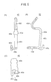
- the press-fitting part 40a is formed with a saw tooth-shape so that a plurality of protruding parts being protruded as triangle structures being press-fitted into the fixing hole 20a from which it would be hard to escape are formed sequentially. Also, after the substrate connector 40b is soldered to a flexible line plate 50, because the substrate connector 40b is bent and manufactured to be small and be U-shaped with a curve, the flexible line plate 50 is kept between the bottom of the housing 12 and the substrate connector 40b.
- the eject operation detecting switch 42 comprises the fixed section (a fixed terminal) 42A to be kept at the connector pin 20 and the mobile section (a mobile terminal) 42B to be kept at the slider 54 described below.
- FIG. 9 is a view that shows a structure of a plate 14, (A) is a bottom plan view of the plate 14, (B) is a front view of the plate 14, (C) is a side view of the plate 14, and (D) is a D-D vertical cross section view of the plate 14.
- Stoppers 14d-14g being press-fitted into the stopper holes 46a-46d of the housing 12 protrude at an under surface of the flat plate part 14a. Also, protruding parts 14h and 14i contacting with the connector pin keeping part 20 of the housing 12 protrude in the plate 14. In addition, not only are the stopper 14d-14g of the plate 14 press-fitted into the stopper hole 46a-46d of the housing 12 but also the protruding part 14h and 14i contact a back surface of the connector pin keeping part 20, and also side plates 14b, 14c contact outer surfaces of the left side part 36 and the right side part 38 so as to be joined with the housing 12.
- a fixing part 14m as a screw stopper is provided on the side plate 14b protruding to a right side direction and a fixing part 14n as a screw stopper is provided on the side plate 14c protruding to left side direction.
- a restriction part 14o restricting lock operation of the lock system 18 protrudes under a surface of the flat plate part 14a. When the insert position of the memory card 24 is an half lock condition as described below, the restriction part 14o does not restrict a cancellation operation of the lock system 18, and when the insert position of the memory card 24 is a full lock condition, the restriction part 14o operates to restrict a cancellation operation of the lock system 18
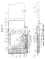
- the lock system 18 has the slider 54, a lock component 56 (a pressured component) to be stopped at the slider 54, a lock pin 58 to be engaged to the slider 54, a plate spring 60 pressing the lock pin 58 to the slider 54 and a coil spring 62 pressing the slider 54 in the eject direction (Yb Direction).
- a lock component 56 a pressured component
- a lock pin 58 to be engaged to the slider 54
- a plate spring 60 pressing the lock pin 58 to the slider 54
- a coil spring 62 pressing the slider 54 in the eject direction (Yb Direction).
- the slider 54 comprises a slide part 54A extending in the inserting direction of a card (Ya direction) and a protruded part 54B protruding from a side of the slider part 54A to the insertion part 22, and formed as one.
- the engagement slot 54b is formed surrounding a heart shaped cum 54e. Then, along with an inserting operation of the memory card 24, the tip 58a of the lock pin 58 slides with tracing the periphery of the heart shaped cum 54e so as to keep the lock component 56 at the full lock position in that the tip 58a of the lock pin 58 is stopped at a concavity 54f of the heart shaped cum 54e. Also, when the full lock condition is cancelled out, the slider 54 slides in the eject direction (Yb direction) pushed by a spring force of a coil spring 62 and the tip 58a of the lock pin 58 passes though the engagement slot 54b and moves to an escape slot 54g, then ejects the memory card 24 to the position as before inserting.
- an escape part 54h that can cancel a lock to the memory card 24 as the lock component 56 of a side surface displaces to the outside is provided on the slider 54.
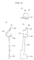
- FIG. 13 is a view that shows a structure of a lock component 56, (A) is a plan view of the lock component 56, (B) is a side view of the lock component 56, and (C) is a rear view of the lock component 56.
- FIG. 14 is a view that shows an inserting position of the memory card 24, (A) is a side section view of a state of the memory card 24 before inserting, (B) is a side sectional view of a state of a half-lock of the memory card 24 after inserting, (C) is a side sectional view of a state of a full-lock of the memory card 24 after inserting, and (D) is a side section view of a state to be inserted where the memory card 24 is inserted into a maximum inserting position.
- a displacement of the lock component 56 to the cancel direction of the lock is not restricted (a direction which the card stopper 56c is separated from the concavity 32 of the memory card 24)
- the card stopper 56c displaces to the direction which is separated from the concavity 32 of the memory card 24 then a stopper according to the lock component 56 is released so as to be able to pull out the memory card 24.
- FIG. 15 is a view that shows a state of the connector for a memory card 11 where the memory card 24 is inserted at the half-lock position
- (A) is a plan view of the connector for a memory card 11
- (B) is a side view of the connector for a memory card 11.
- FIG. 16 is a view which shows a state of the connector for a memory card 11 where the memory card 24 is inserted at the full-lock position
- (A) is a plan view of the connector for a memory card 11
- (B) is a side view of the connector for a memory card 11.
- the slider 54 moves to the eject direction (Yb direction) by a spring force of the coil spring 62 and directly contacts with the step 36b of the housing 12, then the lock component 56 makes the card stopper 56c protrude to a side of the insertion part 22, and the protruded part 56d is stopped at the stopper 48a of the concavity 48 provided on the housing 12. Also, the tip 58a of the lock pin 58 fits into the escape slot 54g of the slider 54.
- the stopper 56e of the lock component 56 is not facing to the restriction part 14o of the plate 14, but faces to the concavity 48 provided on the left side part 36 of the housing 12, and the lock can be released by displacing to an outside direction in order to go into the concavity 48.
- the lock component 56 permits an insertion of the memory card 24 by displacing of the card stopper 56c to a side direction of the insertion part 22, also the lock component 56 guides an inserting operation by pressing a side surface of the memory card 24.
Landscapes
- Coupling Device And Connection With Printed Circuit (AREA)
Abstract
Description
Claims (6)
- A connector for a memory card comprising:a housing forming an insertion part into which a memory card is inserted;a connector pin keeping part provided on a side end of the insertion part of said housing;a connector pin inserting hole being penetrated in a direction of a thickness of said connector pin keeping part; anda connector pin that is formed so as to have one end of said connector pin being extended in the direction of thickness so as to be inserted into said connector pin inserting hole and the other end of said connector pin being extended in a moving direction of the memory card.
- The connector for a memory card as claimed in claim 1, characterized in that said connector pin keeping part is formed so as to be horizontally bridged to the insertion part of said housing and a plurality of connector pin inserting holes are juxtaposed.
- The connector for a memory card as claimed in claim 1, characterized in that said connector pin comprises:a press-fitting part being press-fitted into the connector pin inserting hole of the connector pin keeping part;a substrate connector part provided on a lower end of said press-fitting part;an arm extending in a horizontal direction by being bent at a substantially right angle from the lower end of said press-fitting part; anda contacting part that contacts with a terminal of said memory card by being bent upward from a tip of said arm then bent to be inclined downward.
- The connector for a memory card as claimed in claim 3, characterized in that said substrate connector part is formed so as to be soldered in a state in which a flexible wiring board is held between said housing and the substrate connector part.
- The connector for a memory card as claimed in claim 3, characterized in that said arm has a stopper protruding on a side so as to restrict a displacement of said contact part.
- The connector for a memory card as claimed in claim 1, characterized in comprising:an eject operation detecting switch constituted by a fixed terminal provided on said connector pin keeping part and a movable terminal that contacts with said fixed terminal with said memory card being inserted into a deep part of said insertion part.
Applications Claiming Priority (3)
| Application Number | Priority Date | Filing Date | Title |
|---|---|---|---|
| JP2000199693 | 2000-06-30 | ||
| JP2000199693A JP4714964B2 (en) | 2000-06-30 | 2000-06-30 | Memory card connector |
| PCT/JP2001/005580 WO2002003503A1 (en) | 2000-06-30 | 2001-06-28 | Connector for memory card |
Publications (3)
| Publication Number | Publication Date |
|---|---|
| EP1229606A1 true EP1229606A1 (en) | 2002-08-07 |
| EP1229606A4 EP1229606A4 (en) | 2005-06-08 |
| EP1229606B1 EP1229606B1 (en) | 2006-09-13 |
Family
ID=18697674
Family Applications (1)
| Application Number | Title | Priority Date | Filing Date |
|---|---|---|---|
| EP01945669A Expired - Lifetime EP1229606B1 (en) | 2000-06-30 | 2001-06-28 | Connector for memory card |
Country Status (5)
| Country | Link |
|---|---|
| US (1) | US6619991B2 (en) |
| EP (1) | EP1229606B1 (en) |
| JP (1) | JP4714964B2 (en) |
| DE (1) | DE60123007T2 (en) |
| WO (1) | WO2002003503A1 (en) |
Families Citing this family (17)
| Publication number | Priority date | Publication date | Assignee | Title |
|---|---|---|---|---|
| US7766517B2 (en) | 2001-06-15 | 2010-08-03 | Apple Inc. | Active enclosure for computing device |
| JP3861121B2 (en) | 2002-01-18 | 2006-12-20 | 日本圧着端子製造株式会社 | Card connector |
| JP3830852B2 (en) * | 2002-04-15 | 2006-10-11 | アルプス電気株式会社 | Card connector device |
| USD482692S1 (en) | 2002-04-22 | 2003-11-25 | Mitsumi Electric Co., Ltd. | Electrical connector for memory card |
| USD482364S1 (en) | 2002-04-22 | 2003-11-18 | Mitsumi Electric Co., Ltd. | Attaching device for memory card |
| USD482693S1 (en) | 2002-05-31 | 2003-11-25 | Mitsumi Electric Co., Ltd. | Attaching device for memory card |
| ATE537585T1 (en) * | 2003-02-19 | 2011-12-15 | Hosiden Corp | CARD CONNECTOR |
| KR100619579B1 (en) * | 2003-05-26 | 2006-09-06 | 마츠시다 덴코 가부시키가이샤 | Connector for memory card |
| JP4403040B2 (en) * | 2004-08-19 | 2010-01-20 | 日本圧着端子製造株式会社 | Card holder for SIM socket |
| TWI242315B (en) * | 2004-11-17 | 2005-10-21 | Excel Cell Elect Co Ltd | Terminal stand |
| JP4202337B2 (en) * | 2005-05-09 | 2008-12-24 | モレックス インコーポレーテッド | Card connector |
| US7037125B1 (en) * | 2005-05-17 | 2006-05-02 | L & K Precision Technology Co., Ltd. | Memory card connector |
| US7344402B2 (en) * | 2006-03-16 | 2008-03-18 | Lenovo Pte. Ltd. | Apparatus and method for component module insertion and removal protection |
| US7396245B2 (en) * | 2006-10-13 | 2008-07-08 | Cheng Uei Precision Industry Co., Ltd. | Memory card connector |
| JP4791389B2 (en) * | 2007-02-22 | 2011-10-12 | ユニオンマシナリ株式会社 | Card connector |
| JP5202414B2 (en) * | 2009-03-26 | 2013-06-05 | 京セラ株式会社 | Portable electronic devices |
| US8939791B2 (en) | 2013-01-27 | 2015-01-27 | International Business Machines Corporation | Primary circuit board non-conductive void having different planar dimensions through board thickness to secure non-conducting locking member of holder |
Family Cites Families (10)
| Publication number | Priority date | Publication date | Assignee | Title |
|---|---|---|---|---|
| US3634806A (en) * | 1969-10-31 | 1972-01-11 | Thomas & Betts Corp | Matched impedance connector |
| FR2600675B1 (en) | 1986-06-24 | 1988-08-26 | Pechiney Aluminium | METHOD FOR ADJUSTING THE PIT CONTENT OF ANODES FOR THE PRODUCTION OF ALUMINUM BY ELECTROLYSIS |
| JPH0338956Y2 (en) * | 1986-06-26 | 1991-08-16 | ||
| US5653610A (en) * | 1994-12-01 | 1997-08-05 | The Whitaker Corporation | Smart card connector with card biasing means |
| US5967833A (en) * | 1996-08-20 | 1999-10-19 | North American Specialties Corporation | Circuit connector with multiple contacts and built in strain relief |
| JP3083778B2 (en) * | 1997-03-10 | 2000-09-04 | エスエムケイ株式会社 | IC card connector |
| JP2973402B2 (en) | 1997-05-19 | 1999-11-08 | 山一電機株式会社 | Card end detecting device in memory card reader |
| JPH11154571A (en) * | 1997-11-21 | 1999-06-08 | Alpha Corp | connector |
| FR2773275B1 (en) * | 1997-12-26 | 2000-01-28 | Itt Mfg Enterprises Inc | VERY LOW THICKNESS ELECTRICAL CONNECTOR FOR CONNECTION OF AN ELECTRONIC MEMORY CARD |
| ES1040916Y (en) * | 1998-07-15 | 1999-11-01 | Mecanismos Aux Ind | PERFECTED MICROTERMINAL. |
-
2000
- 2000-06-30 JP JP2000199693A patent/JP4714964B2/en not_active Expired - Fee Related
-
2001
- 2001-06-28 US US10/070,096 patent/US6619991B2/en not_active Expired - Fee Related
- 2001-06-28 WO PCT/JP2001/005580 patent/WO2002003503A1/en not_active Ceased
- 2001-06-28 EP EP01945669A patent/EP1229606B1/en not_active Expired - Lifetime
- 2001-06-28 DE DE60123007T patent/DE60123007T2/en not_active Expired - Lifetime
Also Published As
| Publication number | Publication date |
|---|---|
| EP1229606B1 (en) | 2006-09-13 |
| DE60123007D1 (en) | 2006-10-26 |
| EP1229606A4 (en) | 2005-06-08 |
| JP2002015797A (en) | 2002-01-18 |
| US20020115351A1 (en) | 2002-08-22 |
| JP4714964B2 (en) | 2011-07-06 |
| US6619991B2 (en) | 2003-09-16 |
| WO2002003503A1 (en) | 2002-01-10 |
| DE60123007T2 (en) | 2007-09-20 |
Similar Documents
| Publication | Publication Date | Title |
|---|---|---|
| EP1229606B1 (en) | Connector for memory card | |
| EP1229611A1 (en) | Connector for memory card | |
| US6527590B2 (en) | Card connector having overstroke for card mounting position | |
| US11043764B2 (en) | Flat-conductor connector | |
| CN101305384B (en) | Card connector | |
| JP4168817B2 (en) | Card connector | |
| US7118395B2 (en) | Card connector locking member arrangement | |
| EP1229614B1 (en) | Connector for memory card | |
| JP3996559B2 (en) | Electronic card connector | |
| US8251720B2 (en) | Push-push card connector | |
| US6869017B2 (en) | Card connector | |
| US6816379B2 (en) | External storage device unit, and information processor having the same | |
| JPH10255905A (en) | IC card connector | |
| US6757173B2 (en) | Card connector assembly | |
| JP4425715B2 (en) | Card connector device | |
| CN100593173C (en) | Low Profile Memory Card Connector | |
| JP3983531B2 (en) | Recording media device | |
| JP2007234465A (en) | Card connector | |
| JP2008243461A (en) | Card connector | |
| KR100998174B1 (en) | Electronic device with card insertion slot | |
| JP2007141719A (en) | Energizing mechanism and memory card connector | |
| JP2003142207A (en) | Card connector | |
| JP2007242527A (en) | Card connector device | |
| JP2003086299A (en) | Card connector | |
| JP4291108B2 (en) | Card connector device |
Legal Events
| Date | Code | Title | Description |
|---|---|---|---|
| PUAI | Public reference made under article 153(3) epc to a published international application that has entered the european phase |
Free format text: ORIGINAL CODE: 0009012 |
|
| 17P | Request for examination filed |
Effective date: 20020301 |
|
| AK | Designated contracting states |
Kind code of ref document: A1 Designated state(s): AT BE CH CY DE DK ES FI FR GB GR IE IT LI LU MC NL PT SE TR |
|
| RBV | Designated contracting states (corrected) |
Designated state(s): AT BE CH CY DE FI FR GB LI |
|
| A4 | Supplementary search report drawn up and despatched |
Effective date: 20050426 |
|
| RIC1 | Information provided on ipc code assigned before grant |
Ipc: 7H 01R 12/18 A Ipc: 7G 06K 13/08 B |
|
| 17Q | First examination report despatched |
Effective date: 20050629 |
|
| GRAP | Despatch of communication of intention to grant a patent |
Free format text: ORIGINAL CODE: EPIDOSNIGR1 |
|
| RBV | Designated contracting states (corrected) |
Designated state(s): DE FI FR GB |
|
| GRAS | Grant fee paid |
Free format text: ORIGINAL CODE: EPIDOSNIGR3 |
|
| GRAA | (expected) grant |
Free format text: ORIGINAL CODE: 0009210 |
|
| AK | Designated contracting states |
Kind code of ref document: B1 Designated state(s): DE FI FR GB |
|
| PG25 | Lapsed in a contracting state [announced via postgrant information from national office to epo] |
Ref country code: FI Free format text: LAPSE BECAUSE OF FAILURE TO SUBMIT A TRANSLATION OF THE DESCRIPTION OR TO PAY THE FEE WITHIN THE PRESCRIBED TIME-LIMIT Effective date: 20060913 |
|
| REG | Reference to a national code |
Ref country code: GB Ref legal event code: FG4D |
|
| REF | Corresponds to: |
Ref document number: 60123007 Country of ref document: DE Date of ref document: 20061026 Kind code of ref document: P |
|
| ET | Fr: translation filed | ||
| PLBE | No opposition filed within time limit |
Free format text: ORIGINAL CODE: 0009261 |
|
| STAA | Information on the status of an ep patent application or granted ep patent |
Free format text: STATUS: NO OPPOSITION FILED WITHIN TIME LIMIT |
|
| 26N | No opposition filed |
Effective date: 20070614 |
|
| PGFP | Annual fee paid to national office [announced via postgrant information from national office to epo] |
Ref country code: FR Payment date: 20100709 Year of fee payment: 10 |
|
| PGFP | Annual fee paid to national office [announced via postgrant information from national office to epo] |
Ref country code: GB Payment date: 20100623 Year of fee payment: 10 Ref country code: DE Payment date: 20100625 Year of fee payment: 10 |
|
| GBPC | Gb: european patent ceased through non-payment of renewal fee |
Effective date: 20110628 |
|
| REG | Reference to a national code |
Ref country code: FR Ref legal event code: ST Effective date: 20120229 |
|
| REG | Reference to a national code |
Ref country code: DE Ref legal event code: R119 Ref document number: 60123007 Country of ref document: DE Effective date: 20120103 |
|
| PG25 | Lapsed in a contracting state [announced via postgrant information from national office to epo] |
Ref country code: DE Free format text: LAPSE BECAUSE OF NON-PAYMENT OF DUE FEES Effective date: 20120103 Ref country code: FR Free format text: LAPSE BECAUSE OF NON-PAYMENT OF DUE FEES Effective date: 20110630 |
|
| PG25 | Lapsed in a contracting state [announced via postgrant information from national office to epo] |
Ref country code: GB Free format text: LAPSE BECAUSE OF NON-PAYMENT OF DUE FEES Effective date: 20110628 |