EP1229570A1 - Hot plate - Google Patents
Hot plate Download PDFInfo
- Publication number
- EP1229570A1 EP1229570A1 EP01938699A EP01938699A EP1229570A1 EP 1229570 A1 EP1229570 A1 EP 1229570A1 EP 01938699 A EP01938699 A EP 01938699A EP 01938699 A EP01938699 A EP 01938699A EP 1229570 A1 EP1229570 A1 EP 1229570A1
- Authority
- EP
- European Patent Office
- Prior art keywords
- ceramic substrate
- heating element
- resistance heating
- ceramic
- hot plate
- Prior art date
- Legal status (The legal status is an assumption and is not a legal conclusion. Google has not performed a legal analysis and makes no representation as to the accuracy of the status listed.)
- Withdrawn
Links
Images




Classifications
-
- H—ELECTRICITY
- H10—SEMICONDUCTOR DEVICES; ELECTRIC SOLID-STATE DEVICES NOT OTHERWISE PROVIDED FOR
- H10P—GENERIC PROCESSES OR APPARATUS FOR THE MANUFACTURE OR TREATMENT OF DEVICES COVERED BY CLASS H10
- H10P72/00—Handling or holding of wafers, substrates or devices during manufacture or treatment thereof
- H10P72/04—Apparatus for manufacture or treatment
- H10P72/0431—Apparatus for thermal treatment
- H10P72/0432—Apparatus for thermal treatment mainly by conduction
-
- H—ELECTRICITY
- H05—ELECTRIC TECHNIQUES NOT OTHERWISE PROVIDED FOR
- H05B—ELECTRIC HEATING; ELECTRIC LIGHT SOURCES NOT OTHERWISE PROVIDED FOR; CIRCUIT ARRANGEMENTS FOR ELECTRIC LIGHT SOURCES, IN GENERAL
- H05B3/00—Ohmic-resistance heating
- H05B3/10—Heating elements characterised by the composition or nature of the materials or by the arrangement of the conductor
- H05B3/12—Heating elements characterised by the composition or nature of the materials or by the arrangement of the conductor characterised by the composition or nature of the conductive material
- H05B3/14—Heating elements characterised by the composition or nature of the materials or by the arrangement of the conductor characterised by the composition or nature of the conductive material the material being non-metallic
- H05B3/141—Conductive ceramics, e.g. metal oxides, metal carbides, barium titanate, ferrites, zirconia, vitrous compounds
- H05B3/143—Conductive ceramics, e.g. metal oxides, metal carbides, barium titanate, ferrites, zirconia, vitrous compounds applied to semiconductors, e.g. wafers heating
-
- H—ELECTRICITY
- H05—ELECTRIC TECHNIQUES NOT OTHERWISE PROVIDED FOR
- H05B—ELECTRIC HEATING; ELECTRIC LIGHT SOURCES NOT OTHERWISE PROVIDED FOR; CIRCUIT ARRANGEMENTS FOR ELECTRIC LIGHT SOURCES, IN GENERAL
- H05B3/00—Ohmic-resistance heating
- H05B3/20—Heating elements having extended surface area substantially in a two-dimensional [2D] plane, e.g. plate-heater
- H05B3/22—Heating elements having extended surface area substantially in a two-dimensional [2D] plane, e.g. plate-heater non-flexible
- H05B3/26—Heating elements having extended surface area substantially in a two-dimensional [2D] plane, e.g. plate-heater non-flexible heating conductor mounted on insulating base
- H05B3/265—Heating elements having extended surface area substantially in a two-dimensional [2D] plane, e.g. plate-heater non-flexible heating conductor mounted on insulating base the insulating base being an inorganic material, e.g. ceramic
Definitions
- the present invention relates to a hot plate mainly used for a semiconductor producing/examining device.
- a heater, a wafer prober and the like in which a base material made of metal such as stainless steel, aluminum alloy is used.
- the heater plate is made of metal, the thickness thereof has to be approximately 1.5mm. The reason is that thin metal plate generates warping, strain and the like by thermal expansion due to heating, so that the silicon wafer placed on the metal plate may be damaged or inclined. However, there has been a problem that, when the heater plate is made too thick, the heater becomes too heavy and bulky.
- a temperature of a face for heating an object to be heated, such as a silicon wafer and the like.
- a heating face since the metal plate has a large thickness, there has been a problem that the temperature of the heater plate does not rapidly follow the change of the voltage or the current amount and the temperature cannot be easily controlled.
- JP Kokai Hei 11-40330 proposes a hot plate in which a nitride ceramic or a carbide ceramic having high heat conductivity and strength is used as a substrate and a resistance heating element is provided on a surface of the plate-formed body made of such a ceramic (i.e., the ceramic substrate) by sintering metal particles on the substrate surface.
- JP Kokai Hei 9-48668 discloses an aluminumnitride sintered body containing carbon.
- thermoviewer when a temperature of a surface thereof on which an object to be heated such as a silicon wafer is heated (hereinafter, referred to as a heating face) is measured by a thermoviewer, infrared ray emitted from the heating element is likely to be measured since infrared ray tends to penetrate the ceramic substrate, so that there has been a problem that the temperature at the heating face cannot be measured accurately.
- a ceramic substrate having infrared ray transmittance of 0% or not more than 10% can be produced by incorporating a given amount of carbon in the ceramic substrate, that is, specifically :by degreasing and firing a raw formed body which is made by pressurizing and forming a ceramic powder and a resin, thus decreasing the crystallinity of the carbon and increasing the efficiency of absorbance of infrared ray; or by selecting a resin which is more likely to remain as carbon with low crystallinity in the degreasing process, so that the present invention has been completed.
- the present invention is a hot plate comprising a ceramic substrate and a conductor layer formed on a surface of the ceramic substrate or inside the ceramic substrate, wherein a transmittance of an infrared ray wavelength of 2500 nm, of the ceramic substrate, is 0% or not more than 10%, and desirably a brightness of the ceramic substrate based on JIS Z 8721 is not more than N6.
- the ceramic substrate does not transmit the infrared ray emitted from the heating element, and the infrared ray from the heating element does not disturb the measurement when the surface temperature of the heating face of the hot plate is measured by the thermoviewer.
- a wavelength for measurement of the thermoviewer can be set from around 2500nm, and the infrared ray having a comparatively short wavelength generating at a low temperature can be captured for the measurement, thus a temperature of the heating face can be measured in a wider range from low temperature to high temperature.
- the brightness based on JIS Z 8721 is not more than N6 so that the ceramic substrate is blackened, thus by utilizing black body radiation and obtaining a high radiation heat, the ceramic substrate can be efficiently heated by the resistance heating element and the like.
- the resistance heating element is formed inside the ceramic substrate, the resistance heating element can be shielded.
- the hot plate of the present invention is a hot plate comprising a ceramic substrate and a conductor layer formed on a surface of the ceramic substrate or inside the ceramic substrate, wherein a transmittance of an infrared ray wavelength, of the above-mentioned ceramic substrate, is 0% or not more than 10%.
- the infrared ray wavelength to be measured may be selected from a range of 760 to 2600nm, but desirably is 2500nm. Since the wavelength is in an intermediate region between a near infrared region (760 to 2500nm) and an intermediate infrared region (2500 to 25000nm), it serves as a standard of transmittance of both infrared ray regions.
- the near infrared ray tends to be generated at a relatively low temperature, however, by curbing the transmittance of the near infrared ray region to not more than 10%, a temperature of a heating face, which ranges from a low temperature to a high temperature (100 to 800°C), can be measured by a thermoviewer more accurately.
- the infrared ray transmittance of the ceramic substrate is reduced to 0 or not more than 10% is that, in the case that the transmittance is over 10%, the infrared ray emitted from the heating element affects the measurement by acting as background, whereby the measurement of the temperature in the heating face can no longer be performed accurately and the measured values exhibit errors.
- the transmittance of the ceramic substrate is most preferably not more than 5%.
- the above-mentioned transmittance is a value in a case of measuring an optical transmittance of a ceramic substrate having a thickness of 0.5mm.
- a brightness of the ceramic substrate is preferably not more than N6 when the brightness is measured according to the prescription of JIS Z 8721, because the ceramic substrate having a brightness of such a degree exhibits excellent heat radiation and shielding property. Further, in the ceramic substrate having such properties, the temperature at the surface thereof can be accurately measured by using a thermoviewer and thus the temperature of the face of the ceramic substrate, for heating a silicon wafer and the like (heating face) , can be easily controlled.
- N of the brightness is specifically indicated by the symbols N0 to N10, which represent ten gradient colors of a specific color. These ten gradient colors are obtained by: setting the brightness of ideal black at 0 and that of ideal white at 10; dividing the brightness range of the specific color into ten sections between the brightness of black and that of white in a manner that the difference in brightness perceived between adjacent sections becomes equal; and allocating the symbols N0 to N10 in this order to the obtained sections as the gradient colors.
- the actual measurement of the brightness is carried out by comparing the sample with color cards corresponding to N0 to N10. In the measurement, the number of the first decimal fraction is set at 0 or 5.
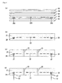
- Fig. 1 is a bottom view which schematically shows one example of a hot plate of the present invention
- Fig. 2 is a partially-enlarged sectional view which schematically shows a part of the hot plate shown in Fig. 1.
- a resistance heating element is formed on the bottom face of the ceramic substrate.
- a ceramic substrate 11 is formed so as to have a disc shape, and at a bottom face 11b of the ceramic substrate 11, a resistance heating element 12a is formed in the vicinity of the peripheral portion of the bottom face and resistance heating elements 12b to 12d are formed at the portion radially inner side of the resistance heating element 12a.
- the resistance heating element 12a is composed of a winding circuit as shown in Fig. 1.
- the resistance heating elements 12b to 12d are composed of circuits having a configuration of substantially concentric circles.
- the ceramic substrate 11 is designed, by combining the above-mentioned circuits, so that the temperature distribution at the heating face 11a is made even.
- a metal covering layer 120 is provided on each of the resistance heating elements 12a to 12d, so that the resistance heating elements are prevented from being oxidized.
- An end portion 13 for input/output is formed at each end of the resistance heating elements 12a to 12d.
- an external terminal 17 is connected to the end portion 13 by solder, as shown in Fig. 2 .
- a socket 170 equipped with wiring is connected to the external terminal 17, whereby the external terminal 17 is connected to a powder source.
- a bottomed hole 14 in which a temperature measuring element 18 is to be inserted is formed at the ceramic substrate 11.
- a through hole 15 through which a lifter pin 16 is to be inserted is formed at a portion near to the center of the ceramic substrate 11.
- the lifter pin 16 is designed so that the lifter pin 16 can be moved in the vertical direction with carrying a silicon wafer 19 put thereon.
- the silicon wafer 19 can be transferred to a carrier machine (not shown) or the silicon wafer 19 can be received from a carrier machine.
- the silicon wafer 19 can be set on a heating face 11a of the ceramic substrate 11 so that the silicon wafer 19 is heated; or the silicon wafer 19 can be supported in a state that the silicon wafer 19 is distanced by the length of 50 to 2000 ⁇ m from the heating face 11a; so that the silicon wafer 19 can be heated.
- the silicon wafer 19 is heated in a state that the silicon wafer 19 is distanced by the length of 50 to 2000 ⁇ m from the heating face 11a by: forming a through hole or a concave portion in the ceramic substrate 11; inserting a supporting pin having a tip end shaped in a form of aspire or semisphere into the through hole or the concave portion; fixedly holding the supporting pin in a state that the supporting pin is slightly projected from the ceramic substrate 11; and supporting the silicon wafer 19 by the supporting pin.
- Fig. 3 is a partially-enlarged sectional view which schematically shows another example of the hot plate of the present invention.
- the resistance heating element is formed inside the ceramic substrate.
- a ceramic substrate 21 is formed so as to have a disc shape (not shown) in a manner similar to that of the ceramic heater shown in Fig. 1.
- a resistance heating element 22 is formed inside the ceramic substrate 21, in the pattern of the combination of concentric circles and winding lines i.e., in the pattern similar to that shown in Fig. 1.
- a conductor-filled through hole 28 is formed right under the end portion of the resistance heating element 22.
- a blind hole 27 is formed on the bottom face 21b of the ceramic substrate 21 such that the conductor-filled through hole 28 is exposed outside.
- An external terminal 23 is inserted in the blind hole 27 and connected thereto by using a brazing-filler 24 and the like.
- a socket having a conductive wire is connected to the external terminal 23 in a manner similar to that in the hot plate shown in Fig. 1.
- the conductive wire is connected to a power source and the like.
- the hot plate of the present invention has a structure shown in each of Figs. 1 to 3, for example.
- Each of the members which compose the above-mentioned hot plate, and the like, will be described one by one in detail hereinafter.
- the ceramic material composing the above-mentioned hot plate is not particularly restricted.
- the ceramic material include nitride ceramic, carbide ceramic, oxide ceramic and the like.
- nitride ceramic examples include metal nitride ceramic such as aluminum nitride, silicon nitride, boronnitride, titanium nitride and the like.
- carbide ceramic examples include metal carbide ceramic such as silicon carbide, zirconium carbide, titanium carbide, tantalum carbide, tungsten carbide and the like.
- oxide ceramic examples include metal oxide ceramic such as alumina, zirconia, cordierite, mullite and the like.
- These ceramics may be used singly or as a combination of 2 or more.
- nitride ceramic and carbide ceramic are more preferable than oxide ceramic, because the heat conductivity of the nitride and carbide ceramics are higher than that of the oxide ceramic.
- the aluminum nitride is the most preferable because the heat conductivity thereof is the highest (180W/m ⁇ K).
- the nitride ceramic contains a metal oxide.
- the metal oxide acts as a sintering aid and thus facilitates the sintering process and reduces the size of the pore present inside the ceramic substrate, whereby the breakdown voltage, the mechanical properties and the like of the ceramic substrate are improved.
- metal oxide examples include yttria (Y 2 O 3 ), alumina (Al 2 O 3 ), rubidium oxide (Rb 2 O), lithium oxide (Li 2 O), calcium oxide (CaCO 3 ) and the like.
- the preferable content of the metal oxide in the nitride ceramic is 1 to 10 parts by weight with respect to 100 parts by weight of the nitride ceramic.
- the infrared ray transmittance is reduced to 0 or not more than 10% and the brightness thereof is not more than N6 when evaluated as the value according to the prescription of JIS Z 8721.
- a ceramic substrate having such properties as described above can be obtained by adding carbon to the ceramic substrate so that the carbon content therein is in a range of 100 to 5000ppm.
- the carbon has two types: amorphous one and crystalline one.
- amorphous carbon is used, the decrease in the volume resistivity of the ceramic substrate at a high temperature can be suppressed.
- amorphous carbon is likely to absorb rays in the infrared region and does not allow such infrared rays to transmit the ceramic substrate. Therefore, amorphous carbon is more advantageously used than crystalline carbon.
- Amorphous carbon can be obtained, for example, by firing in the air a hydrocarbon (preferably a saccharide) which is composed of only C, H and O.
- a hydrocarbon preferably a saccharide
- Examples of crystalline carbon includes graphite powder and the like.
- a ceramic substrate containing carbon can be obtained by heat-decomposing a green sheet lamination and the like which contains an acrylic resin in an inactive atmosphere and then heating and pressurizing the product.
- the degree of crystallinity (or amorphousness) can be adjusted by changing the acid value of the acrylic resin.
- the above-mentioned acrylic resin may be added as a binder.
- acrylic resin binder As the above-mentioned acrylic resin binder, the SA-545 series manufactured by Mitsui Chemicals Co., Ltd., or the KC-600 series manufactured by Kyoeisha Co., Ltd., for example, and the like can be used.
- the porosity of the above-mentioned ceramic substrate is not more than 5% and the diameter of the largest pore in the ceramic substrate is not more than 50 ⁇ m.
- the porosity of the ceramic substrate is preferably 0 or not more than 3%.
- the diameter of the largest pore of the ceramic substrate is preferably 0 or not more than 10 ⁇ m.
- the measurement of the pore diameter of the largest pore is performed by: preparing five samples and polishing the surface thereof into mirror planes; photographing the surface of each sample at ten sites by an electron microscope with 2000 to 5000 magnification; selecting the largest pore diameter from each shot; and regarding the average of the largest pore diameter of the 50 shots as the pore diameter of the largest pore.
- the above-mentioned porosity is measured by the Archimedes' method.
- This method includes the steps of: pulverizing the sintered body and putting the pulverized sample into an organic solvent or mercury, to measure the volume thereof; obtaining the true specific gravity from the weight of the pulverized sample and the volume thereof; and calculating the porosity from the obtained true specific gravity and the apparent specific gravity.
- the hot plate of the present invention is generally provided with a resistance heating element as shown in Fig. 1.
- Examples of the above-mentioned temperature controlling means include a Peltier device, in addition to the resistance heating element.
- the resistance heating element is provided inside the ceramic substrate, plural layers of the resistance heating element may be provided therein.
- the patterns at the layers are designed so that the patterns complement each other, whereby any portion thereof is covered by one of these patterns or layers without leaving any uncovered portion when viewed from the top of the heating face.
- a structure having a staggered arrangement may be used.
- the resistance heating element examples include a sintered body of metal or electrically conductive ceramic, a metal foil, a metal wire and the like.
- a metal sintered body which is composed of at least one type selected from tungsten and molybdenum is preferable, because these metals are relatively less likely to be oxidized and have a sufficient resistance value for generating heat.
- the conductive ceramic at least one type selected from carbides of tungsten and molybdenum may be used.
- the resistance heating element is formed at the bottom face of the ceramic substrate, it is preferable to use noblemental (gold, silver, palladium, platinum) or nickel as the metal sintered body. Specifically, silver, silver-palladium and the like can be preferably used.
- the shape of the metal particles used for producing the metal sintered body may be either spherical or scaly. Alternatively, both spherical particles and scaly particles may be used in a mixed manner.
- a metal oxide may be added to the metal sintered body.
- the metal oxide is used in order to adhere the metal particles to the ceramic substrate.
- the reason why the metal oxide improves the adhesion of the metal particles to the ceramic substrate is not clearly known.
- a thin oxidized film is formed on the surface of the metal particle, and an oxidized film is also formed on the surface of the ceramic substrate, regardless of whether the ceramic substrate is oxide ceramic or non-oxide ceramic. It is thus assumed that the oxidized film of the metal particle and that of the ceramic substrate are integrated to one film when these oxidized films are sintered at the surface of the ceramic substrate by way of the metal oxide, whereby the metal particles tightly adhere to the ceramic substrate.
- the metal oxide at least one type of compound selected from the group consisting of lead oxide, zinc oxide, silica, boron oxide (B 2 O 3 ), alumina, yttria and titania is preferably used, because these oxides can improve adhesion of the metal particles to the ceramic substrate without increasing the resistance value of the resistance heating element.
- the content of the metal oxide is preferably in a range of 0.1 or more and less than 10 parts by weight with respect to 100 parts by weight of the metal particles.
- the contents of lead oxide, zinc oxide, silica, boron oxide (B 2 O 3 ), alumina, yttria and titania are preferably 1 to 10 parts by weight in lead oxide, 1 to 30 parts by weight in silica, 5 to 50 parts by weight in boron oxide, 20 to 70 parts by weight in zinc oxide, 1 to 10 parts by weight in alumina, 1 to 50 parts by weight in yttria and 10 to 50 parts by weight in titania, with respect to the whole weight of the metal oxides expressed as 100 parts by weight. It is preferable that these contents of the metal oxides are adjusted so that the total sum of the metal oxides does not exceed 100 parts by weight, because these metal oxides can especially enhance adhesion to the ceramic substrate in such a range.
- the surface of the resistance heating element 12 is preferably covered with a metal covering layer 120 (refer to Fig. 2).
- a metal covering layer 120 As the resistance heating element 12 is a sintered body of metal particles, the resistance heating element 12 is easily oxidized if it is exposed in the air, and the resistance value thereof changes due to the oxidization. By covering the surface of the resistance heating element 12 with a metal covering layer 120, such oxidization can be prevented.
- the thickness of the metal covering layer 120 is preferably in a range of 0.1 to 10 ⁇ m. When the thickness of the metal covering layer 120 is within this range, the oxidization of the resistance heating element can be prevented without changing the resistance value of the resistance heating element too much.
- the metal used for the metal covering layer is not particularly limited, as long as the metal is non-oxidizable. Specific examples thereof include at least one type of metal selected from the group consisting of gold, silver, palladium, platinum and nickel. Among these examples, nickel is the most preferable.
- the resistance heating element requires a terminal for performing connection of the resistance heating element to the power source, and this terminal is attached to the resistance heating element through solder. Nickel effectively prevents the heat dissipation due to solder.
- a terminal pin made of Kovar can be used as the connection terminal.
- the resistance heating element is formed inside the heater plate, the surface of the resistance heating element is not oxidized and thus no covering by the metal layer is required.
- the resistance heating element is formed inside the heater plate, a portion of the surface of the resistance heating element may be exposed outside of the heater plate.
- the metal foil used as the resistance heating element include a resistance heating element produced by a pattern-forming process, such as etching and the like, of nickel foil or stainless foil.
- the metal foils which have been subjected to the pattern-forming process may be laminated with a resin film and the like.
- Example of the metal wire include a tungsten wire, a molybdenum wire and the like.
- thermocontrol means In a case that a Peltier device is used as the temperature controlling means, either heating or cooling can be performed by the same element by changing the flow direction of the current, which is advantageous.
- the Peltier device is formed by connecting p-type and n-type thermoelectric elements in series and attaching these thermoelectric elements to the ceramic plate and the like.
- Peltier device examples include the silicon/germanium-based Peltier device, the bismuth/antimony-based Peltier device, the lead/tellurium-based Peltier device and the like.
- a connecting unit (a conductor-filled through hole) 28 for performing connection of the resistance heating element 22 to the external terminal is required.
- the conductor-filled through hole 28 is formed by filling a metal having a high melting point such as tungsten paste and molybdenum paste or a conductive ceramic such as tungsten carbide and molybdenum carbide.
- the diameter of the connecting unit (a conductor-filled through holes) 28 is preferably in a range of 0.1 to 10mm, because when the diameter of the connection portion is within this range, not only disconnection of the wire but also generation of cracks or strains can be reliably prevented.
- An external terminal pin 23 is connected thereto through the conductor-filled through hole as a connection pad (refer to Fig. 3).
- connection is carried out by using solder or brazing filler.
- the brazing filler silver braze, palladium braze, aluminum braze and gold braze are preferably used.
- gold braze Au-Ni alloy is preferable because Au-Ni alloy exhibits excellent adhesion property with tungsten.
- the ratio of Au/Ni is preferably [81.5 to 82.5 (% by weight)]/[18.5 to 17.5 (% by weight)].
- the thickness of the Au-Ni layer is preferably in a range of 0.1 to 50 ⁇ m, because the connection property is reliably obtained when the thickness of the Au-Ni layer is within this range.
- the alloy exhibits deterioration when used in a highly vacuumed state of 10 -6 to 10 -5 Pa at a high temperature in a range of 500 to 1000°C.
- the Au-Ni alloy does not exhibit deterioration when the alloy is used in such a harsh condition, which is advantageous.
- the content of the impurity elements contained in the Au-Ni alloy is preferably less than 1 parts by weight when the whole weight of the Au-Ni alloy is expressed as 100 parts by weight.
- thermocouple may be embedded in the bottomed hole 12 of the ceramic substrate 1, according to the necessity.
- the temperature of the resistance heating element can be measured by the thermocouple, so that the temperature of the resistance heating element can be controlled by changing the magnitude of the voltage and the current on the basis of the obtained data.
- the size of the connecting portion of the metal wire of the thermocouple is preferably the same as or larger than the strand diameter of each metal wire, but not more than 0.5mm.
- the heat capacity of the connecting portion is made small by such a structure, whereby the temperature is converted into the current value correctly and rapidly. As a result, the temperature controlling property is improved, whereby the temperature distribution at the heating face of the wafer is made small.
- thermocouple examples include the K-type, the R-type, the B-type, the S-type, the E-type, the J-type and the T-type thermocouples, as is raised in JIS-C-1602 (1980).
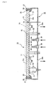
- Fig. 4 is a sectional view which schematically shows a supporting case 30 in which the hot plate (the ceramic substrate) having a structure as described above is fitted.
- the supporting case 30 is designed such that the ceramic substrate 11 is fitted therein through a heat insulator 35 and fixed thereto by a bolt 38 and a holding metal member 37.
- a guide pipe 32 is provided under the portion where the through hole 15 of the ceramic substrate 11 has been formed, so that the guide pipe 32 communicates with the through hole.
- a coolant outlet 30a is formed in the supporting case 31 such that the coolant introduced from a coolant introducing pipe 39 is discharged outside from a coolant outlet 30a. By the action of the coolant, the ceramic substrate 11 can be cooled.
- the resistance heating element is substantially the only component provided on the surface of the ceramic substrate.
- the object to be heated such as a silicon wafer can be heated to a predetermined temperature.
- the hot plate of the present invention is a device mainly used for production/inspection of a semiconductor, which includes as main components a ceramic substrate and a resistance heating element solely provided on the ceramic substrate.
- the device when electrostatic electrodes are provided inside the ceramic substrate, the device functions as an electrostatic chuck.
- a conductor layer is provided on the surface of the ceramic substrate; and a guard electrode and a ground electrode are provided inside the ceramic substrate, the device functions as a wafer prober.
- an electrostatic chuck can be manufactured by providing electrostatic electrodes inside the ceramic substrate, and a wafer prober can be manufactured by providing a chuck top conductor layer at the heating face of the ceramic substrate and also providing a guard electrode and a ground electrode inside the ceramic substrate.
- Equipment of electrodes inside the ceramic substrate can be achieved by embedding a metal foil and the like inside the ceramic substrate.
- a conductor layer can be formed at the surface of the ceramic substrate by using the spattering method or the plating method or employing both of the two methods.
- a hot plate was produced in a manner similar to that of example 2 except that 4 parts by weight of acrylic resin binder (KC-600TM series having the acid value of 17, manufactured by Kyoeisha Co., Ltd.,) was used.
- acrylic resin binder KC-600TM series having the acid value of 17, manufactured by Kyoeisha Co., Ltd.
- examples 4 a hot plate was produced in a manner similar to that of example 2 except that 20 parts by weight of the same acrylic resin binder was used.
- Comparative example 1 was performed in a manner similar to that of example 1 except that the degreasing process was carried out at 600°C for 24 hours and the carbon content was reduced to approximately 100ppm.
- Comparative example 2 was performed in a manner similar to that of example 1 except that crystalline graphite was added.
- the content of the added crystalline graphite in the sintered body was 800ppm.
- the crystallinity of carbon was analyzed by using laser Raman spectrum. A peak was observed at 1580cm -1 . Accordingly, it was confirmed that the carbon was highly crystalline.
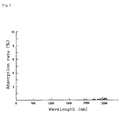
- Fig. 7 shows the transmittance at each wavelength observed in the sintered body (thickness: 0.5mm) of example 1.
- Fig. 8 shows the transmittance at each wavelength observed in the sintered body (thickness: 0.5mm) of comparative example 1.
- t represents the thickness (mm) of the sample.
- S is given by the following formulas (2) and (3).
- r 1 represents the radius of the main electrode
- r 2 represents the inner size (radius) of the guard electrode
- r 3 represents the outer size (radius) of the guard electrode
- D 1 represents the diameter of the main electrode
- D 2 represents the inner size (diameter) of the guard electrode
- D 3 represents the outer size (diameter) of the guard electrode.
- the sintered body according to example 1 hardly has the absorbance of the wavelength in the infrared region, while the sintered body according to comparative example 1 exhibits a quite a high absorption rate of approximately 20% of the wavelength in the infrared region.
- the temperature at the heating face can be accurately measured by a thermoviewer if the transmittance of infrared ray (2500nm) was reduced to not more than 10%.
- the infrared ray transmittance of the ceramic substrate is not more than 10%, this is low. As a result, the temperature at the heating face of the ceramic substrate can be accurately measured by a thermoviewer. Further, in the hot plate according to the present invention, as the ceramic substrate thereof is sufficiently blackened so as to have a brightness of not more than N6, high radiation heat can be obtained.
Landscapes
- Chemical & Material Sciences (AREA)
- Engineering & Computer Science (AREA)
- Ceramic Engineering (AREA)
- Resistance Heating (AREA)
- Surface Heating Bodies (AREA)
- Testing Or Measuring Of Semiconductors Or The Like (AREA)
- Ceramic Products (AREA)
- Physical Vapour Deposition (AREA)
- Chemical Vapour Deposition (AREA)
Abstract
Description
wherein a transmittance of an infrared ray wavelength of 2500 nm, of the ceramic substrate, is 0% or not more than 10%, and desirably a brightness of the ceramic substrate based on JIS Z 8721 is not more than N6.
- 10
- Hot plate
- 11, 21
- Ceramic substrate
- 11a
- Heating face
- 11b, 12b
- Bottom surface
- 12(12a to 12d), 22
- Resistance heating element
- 13
- End portion
- 14
- Bottomed hole
- 15
- Through hole
- 16
- Lifter pin
- 17
- External terminal
- 18
- Temperature measuring element
- 19
- Silicon wafer
- 23
- External terminal
- 24
- Brazing-filler
- 27
- Blind hole
- 28
- Conductor-filled through hole
- 30
- Supporting case
- 32
- Guide pipe
- 35
- Heat insulator
- 37
- Holding metal member
- 38
- Bolt
- 39
- Coolant introducing pipe
| Carbon content (ppm) | Brightness | Transmittance (%) | Volume resistivity (Ω·cm) | Temperature difference (Thermoviewer) (°C) | Temperature difference (Silicon wafer) (°C) | |
| Ex. 1 | 800 | N3.5 | 0.2 | 11×1010 | 5 | 5 |
| Ex. 2 | 900 | N3.5 | 0.1 | 10×1010 | 6 | 6 |
| Ex. 3 | 400 | N3.5 | 5.0 | 13×1010 | 7 | 5 |
| Ex. 4 | 1800 | N3.5 | 0 | 9×10¹⁰ | 6 | 6 |
| Comp. Ex. 1 | 100 | N7.0 | 28 | 18×1010 | 12 | 6 |
| Comp. Ex. 2 | 800 | N3.5 | 15 | 2×10¹⁰ | 11 | 6 |
Claims (3)
- A hot plate comprising a ceramic substrate and a conductor layer formed on a surface of said ceramic substrate or inside said ceramic substrate,
wherein a transmittance of an infrared ray wavelength, of said ceramic substrate, is 0% or not more than 10%. - The hot plate according to claim 1,
wherein a brightness, based on JIS Z 8721, of said ceramic substrate is not more than N6. - The hot plate according to claim 1 or 2,
wherein said infrared ray wavelength is 2500nm.
Applications Claiming Priority (3)
| Application Number | Priority Date | Filing Date | Title |
|---|---|---|---|
| JP2000180321 | 2000-06-15 | ||
| JP2000180321A JP3618640B2 (en) | 2000-06-15 | 2000-06-15 | Hot plate for semiconductor manufacturing and inspection equipment |
| PCT/JP2001/005139 WO2001097263A1 (en) | 2000-06-15 | 2001-06-15 | Hot plate |
Publications (2)
| Publication Number | Publication Date |
|---|---|
| EP1229570A1 true EP1229570A1 (en) | 2002-08-07 |
| EP1229570A4 EP1229570A4 (en) | 2003-02-12 |
Family
ID=18681447
Family Applications (1)
| Application Number | Title | Priority Date | Filing Date |
|---|---|---|---|
| EP01938699A Withdrawn EP1229570A4 (en) | 2000-06-15 | 2001-06-15 | HOTPLATE |
Country Status (4)
| Country | Link |
|---|---|
| US (1) | US20030080110A1 (en) |
| EP (1) | EP1229570A4 (en) |
| JP (1) | JP3618640B2 (en) |
| WO (1) | WO2001097263A1 (en) |
Cited By (1)
| Publication number | Priority date | Publication date | Assignee | Title |
|---|---|---|---|---|
| EP1440957A3 (en) * | 1999-12-28 | 2005-01-05 | Ibiden Co., Ltd. | Ceramic heater |
Families Citing this family (19)
| Publication number | Priority date | Publication date | Assignee | Title |
|---|---|---|---|---|
| US6900149B1 (en) * | 1999-09-06 | 2005-05-31 | Ibiden Co., Ltd. | Carbon-containing aluminum nitride sintered compact and ceramic substrate for use in equipment for manufacturing or inspecting semiconductor |
| WO2001062686A1 (en) * | 2000-02-24 | 2001-08-30 | Ibiden Co., Ltd. | Aluminum nitride sintered compact, ceramic substrate, ceramic heater and electrostatic chuck |
| JP2001247382A (en) * | 2000-03-06 | 2001-09-11 | Ibiden Co Ltd | Ceramic substrate |
| EP1233651A1 (en) * | 2000-04-07 | 2002-08-21 | Ibiden Co., Ltd. | Ceramic heater |
| US7071551B2 (en) * | 2000-05-26 | 2006-07-04 | Ibiden Co., Ltd. | Device used to produce or examine semiconductors |
| JP3516392B2 (en) * | 2000-06-16 | 2004-04-05 | イビデン株式会社 | Hot plate for semiconductor manufacturing and inspection equipment |
| WO2002009171A1 (en) * | 2000-07-25 | 2002-01-31 | Ibiden Co., Ltd. | Ceramic substrate for semiconductor manufacture/inspection apparatus, ceramic heater, electrostatic clampless holder, and substrate for wafer prober |
| US6825448B2 (en) * | 2003-05-01 | 2004-11-30 | Applied Materials, Inc. | Low residual-stress brazed terminal for heater |
| US20060088692A1 (en) * | 2004-10-22 | 2006-04-27 | Ibiden Co., Ltd. | Ceramic plate for a semiconductor producing/examining device |
| US7696455B2 (en) * | 2006-05-03 | 2010-04-13 | Watlow Electric Manufacturing Company | Power terminals for ceramic heater and method of making the same |
| JP4421595B2 (en) | 2006-11-16 | 2010-02-24 | 日本碍子株式会社 | Heating device |
| TWI397967B (en) * | 2010-05-28 | 2013-06-01 | 台灣積體電路製造股份有限公司 | Wafer-level reflow soldering apparatus and method of manufacturing solder sphere and flip chip assembly |
| CN109156050A (en) * | 2016-04-07 | 2019-01-04 | 美题隆公司 | Beryllium oxide integral resistance heater |
| KR102527439B1 (en) * | 2019-03-26 | 2023-04-28 | 니뽄 도쿠슈 도교 가부시키가이샤 | Electrode embedded member and its manufacturing method, electrostatic chuck, ceramic heater |
| DE102019107857A1 (en) * | 2019-03-27 | 2020-10-01 | Aixtron Se | Heating device for a susceptor of a CVD reactor |
| JP7338441B2 (en) * | 2019-12-13 | 2023-09-05 | ウシオ電機株式会社 | light heating device |
| JP7500007B2 (en) * | 2020-03-10 | 2024-06-17 | 日本特殊陶業株式会社 | Holding member and manufacturing method thereof |
| CN113800889B (en) * | 2021-09-10 | 2022-10-28 | 厦门海洋芯科技有限公司 | Carbon Hertz film and application thereof |
| WO2025205677A1 (en) * | 2024-03-29 | 2025-10-02 | リンテック株式会社 | Wiring sheet |
Family Cites Families (11)
| Publication number | Priority date | Publication date | Assignee | Title |
|---|---|---|---|---|
| CN1139117C (en) * | 1995-03-20 | 2004-02-18 | 株式会社东芝 | Silicon nitride circuit substrate |
| EP0757023B1 (en) * | 1995-08-03 | 2000-10-18 | Ngk Insulators, Ltd. | Aluminum nitride sintered bodies and their production method |
| JP3037883B2 (en) * | 1995-08-03 | 2000-05-08 | 日本碍子株式会社 | Aluminum nitride sintered body, method for manufacturing the same and apparatus for manufacturing semiconductor |
| JP3670416B2 (en) * | 1995-11-01 | 2005-07-13 | 日本碍子株式会社 | Metal inclusion material and electrostatic chuck |
| DE19746844C1 (en) * | 1997-10-23 | 1998-12-03 | Schott Glas | Ceramic heating element for electric cooking hob |
| US6077557A (en) * | 1998-11-20 | 2000-06-20 | General Mills, Inc. | Gel products fortified with calcium and method of preparation |
| US6383962B1 (en) * | 1999-03-17 | 2002-05-07 | Asahi Techno Glass Corporation | Aluminum nitride sintered product |
| JP2001118664A (en) * | 1999-08-09 | 2001-04-27 | Ibiden Co Ltd | Ceramic heater |
| US6900149B1 (en) * | 1999-09-06 | 2005-05-31 | Ibiden Co., Ltd. | Carbon-containing aluminum nitride sintered compact and ceramic substrate for use in equipment for manufacturing or inspecting semiconductor |
| JP3228924B2 (en) * | 2000-01-21 | 2001-11-12 | イビデン株式会社 | Ceramic heater for semiconductor manufacturing and inspection equipment |
| JP2001244320A (en) * | 2000-02-25 | 2001-09-07 | Ibiden Co Ltd | Ceramic substrate and method of manufacturing the same |
-
2000
- 2000-06-15 JP JP2000180321A patent/JP3618640B2/en not_active Expired - Lifetime
-
2001
- 2001-06-15 WO PCT/JP2001/005139 patent/WO2001097263A1/en not_active Ceased
- 2001-06-15 EP EP01938699A patent/EP1229570A4/en not_active Withdrawn
- 2001-06-15 US US10/048,979 patent/US20030080110A1/en not_active Abandoned
Cited By (1)
| Publication number | Priority date | Publication date | Assignee | Title |
|---|---|---|---|---|
| EP1440957A3 (en) * | 1999-12-28 | 2005-01-05 | Ibiden Co., Ltd. | Ceramic heater |
Also Published As
| Publication number | Publication date |
|---|---|
| JP3618640B2 (en) | 2005-02-09 |
| JP2001357965A (en) | 2001-12-26 |
| EP1229570A4 (en) | 2003-02-12 |
| WO2001097263A1 (en) | 2001-12-20 |
| US20030080110A1 (en) | 2003-05-01 |
Similar Documents
| Publication | Publication Date | Title |
|---|---|---|
| US20030080110A1 (en) | Hot plate | |
| US6929874B2 (en) | Aluminum nitride sintered body, ceramic substrate, ceramic heater and electrostatic chuck | |
| US6964812B2 (en) | Carbon-containing aluminum nitride sintered compact and ceramic substrate for use in equipment for manufacturing or inspecting semiconductor | |
| EP1435655A2 (en) | Electrostatic chuck | |
| US6849938B2 (en) | Ceramic substrate for semiconductor production and inspection | |
| EP1229571B1 (en) | Hot plate | |
| EP1286390A1 (en) | Ceramic substrate for semiconductor fabricating device | |
| US6884972B2 (en) | Ceramic plate for a semiconductor producing/inspecting apparatus | |
| EP1189274A1 (en) | Ceramic board for semiconductor production and inspection devices | |
| EP1274124A1 (en) | Ceramic substrate | |
| EP1280380A1 (en) | Ceramic board | |
| US20040222211A1 (en) | Carbon-containing aluminum nitride sintered body, and ceramic substrate for a semiconductor producing/examining device | |
| JP2001247382A (en) | Ceramic substrate | |
| JP2001219331A (en) | Electrostatic chuck | |
| EP1440957A2 (en) | Ceramic heater | |
| JP2001319967A (en) | Method for manufacturing ceramic substrate | |
| JP2004214690A (en) | Ceramic substrate for semiconductor manufacturing and inspection device | |
| JP2003208967A (en) | Hot plate | |
| US20060088692A1 (en) | Ceramic plate for a semiconductor producing/examining device | |
| JP2001308168A (en) | Ceramic substrate for semiconductor manufacturing and inspecting device | |
| JP2001313330A (en) | Ceramic board for semiconductor manufacturing-checking apparatus | |
| JP2003100818A (en) | Support container and semiconductor-manufacturing/ inspecting apparatus | |
| JP2003249545A (en) | Ceramic substrate for semiconductor manufacturing and inspection apparatus | |
| JP2002255652A (en) | Ceramic substrate | |
| JP2001345371A (en) | Supporting container, and semiconductor manufacturing and inspecting apparatus |
Legal Events
| Date | Code | Title | Description |
|---|---|---|---|
| PUAI | Public reference made under article 153(3) epc to a published international application that has entered the european phase |
Free format text: ORIGINAL CODE: 0009012 |
|
| 17P | Request for examination filed |
Effective date: 20020311 |
|
| AK | Designated contracting states |
Kind code of ref document: A1 Designated state(s): AT BE CH CY DE DK ES FI FR GB GR IE IT LI LU MC NL PT SE TR |
|
| A4 | Supplementary search report drawn up and despatched |
Effective date: 20030103 |
|
| RIC1 | Information provided on ipc code assigned before grant |
Ipc: 7H 01L 21/00 B Ipc: 7H 05B 3/20 B Ipc: 7H 05B 3/18 B Ipc: 7H 05B 3/16 B Ipc: 7H 01L 21/02 A Ipc: 7H 05B 3/28 B Ipc: 7H 05B 3/26 B Ipc: 7H 05B 3/14 B Ipc: 7H 01L 21/66 B Ipc: 7H 05B 3/10 B |
|
| 17Q | First examination report despatched |
Effective date: 20030521 |
|
| GRAP | Despatch of communication of intention to grant a patent |
Free format text: ORIGINAL CODE: EPIDOSNIGR1 |
|
| STAA | Information on the status of an ep patent application or granted ep patent |
Free format text: STATUS: THE APPLICATION IS DEEMED TO BE WITHDRAWN |
|
| 18D | Application deemed to be withdrawn |
Effective date: 20050609 |