EP1229349A2 - Led illumination device for a scannerless range imaging system - Google Patents
Led illumination device for a scannerless range imaging system Download PDFInfo
- Publication number
- EP1229349A2 EP1229349A2 EP02075242A EP02075242A EP1229349A2 EP 1229349 A2 EP1229349 A2 EP 1229349A2 EP 02075242 A EP02075242 A EP 02075242A EP 02075242 A EP02075242 A EP 02075242A EP 1229349 A2 EP1229349 A2 EP 1229349A2
- Authority
- EP
- European Patent Office
- Prior art keywords
- led
- illumination device
- phase
- illumination
- light emitting
- Prior art date
- Legal status (The legal status is an assumption and is not a legal conclusion. Google has not performed a legal analysis and makes no representation as to the accuracy of the status listed.)
- Withdrawn
Links
Images




Classifications
-
- G—PHYSICS
- G01—MEASURING; TESTING
- G01S—RADIO DIRECTION-FINDING; RADIO NAVIGATION; DETERMINING DISTANCE OR VELOCITY BY USE OF RADIO WAVES; LOCATING OR PRESENCE-DETECTING BY USE OF THE REFLECTION OR RERADIATION OF RADIO WAVES; ANALOGOUS ARRANGEMENTS USING OTHER WAVES
- G01S17/00—Systems using the reflection or reradiation of electromagnetic waves other than radio waves, e.g. lidar systems
- G01S17/87—Combinations of systems using electromagnetic waves other than radio waves
-
- G—PHYSICS
- G01—MEASURING; TESTING
- G01S—RADIO DIRECTION-FINDING; RADIO NAVIGATION; DETERMINING DISTANCE OR VELOCITY BY USE OF RADIO WAVES; LOCATING OR PRESENCE-DETECTING BY USE OF THE REFLECTION OR RERADIATION OF RADIO WAVES; ANALOGOUS ARRANGEMENTS USING OTHER WAVES
- G01S17/00—Systems using the reflection or reradiation of electromagnetic waves other than radio waves, e.g. lidar systems
- G01S17/02—Systems using the reflection of electromagnetic waves other than radio waves
- G01S17/06—Systems determining position data of a target
- G01S17/08—Systems determining position data of a target for measuring distance only
- G01S17/32—Systems determining position data of a target for measuring distance only using transmission of continuous waves, whether amplitude-, frequency-, or phase-modulated, or unmodulated
-
- G—PHYSICS
- G01—MEASURING; TESTING
- G01S—RADIO DIRECTION-FINDING; RADIO NAVIGATION; DETERMINING DISTANCE OR VELOCITY BY USE OF RADIO WAVES; LOCATING OR PRESENCE-DETECTING BY USE OF THE REFLECTION OR RERADIATION OF RADIO WAVES; ANALOGOUS ARRANGEMENTS USING OTHER WAVES
- G01S17/00—Systems using the reflection or reradiation of electromagnetic waves other than radio waves, e.g. lidar systems
- G01S17/88—Lidar systems specially adapted for specific applications
- G01S17/89—Lidar systems specially adapted for specific applications for mapping or imaging
- G01S17/894—Three-dimensional [3D] imaging with simultaneous measurement of time-of-flight at a two-dimensional [2D] array of receiver pixels, e.g. time-of-flight cameras or flash lidar
-
- G—PHYSICS
- G01—MEASURING; TESTING
- G01S—RADIO DIRECTION-FINDING; RADIO NAVIGATION; DETERMINING DISTANCE OR VELOCITY BY USE OF RADIO WAVES; LOCATING OR PRESENCE-DETECTING BY USE OF THE REFLECTION OR RERADIATION OF RADIO WAVES; ANALOGOUS ARRANGEMENTS USING OTHER WAVES
- G01S7/00—Details of systems according to groups G01S13/00, G01S15/00, G01S17/00
- G01S7/48—Details of systems according to groups G01S13/00, G01S15/00, G01S17/00 of systems according to group G01S17/00
- G01S7/481—Constructional features, e.g. arrangements of optical elements
- G01S7/4814—Constructional features, e.g. arrangements of optical elements of transmitters alone
-
- G—PHYSICS
- G01—MEASURING; TESTING
- G01S—RADIO DIRECTION-FINDING; RADIO NAVIGATION; DETERMINING DISTANCE OR VELOCITY BY USE OF RADIO WAVES; LOCATING OR PRESENCE-DETECTING BY USE OF THE REFLECTION OR RERADIATION OF RADIO WAVES; ANALOGOUS ARRANGEMENTS USING OTHER WAVES
- G01S7/00—Details of systems according to groups G01S13/00, G01S15/00, G01S17/00
- G01S7/48—Details of systems according to groups G01S13/00, G01S15/00, G01S17/00 of systems according to group G01S17/00
- G01S7/491—Details of non-pulse systems
- G01S7/4911—Transmitters
Definitions
- the present invention relates to the field of three-dimensional image capture and in particular to a modulated illumination source used in the capture of image depth information with a scannerless range imaging system.
- a scannerless range imaging system having a modulated illumination source and a modulated image receiver.
- a scannerless range imaging system uses an amplitude-modulated high-power laser diode to simultaneously illuminate a target area.
- Conventional optics confine the target beam and image the target onto a receiver, which includes an integrating detector array sensor having hundreds of elements in each dimension.
- the range to a target is determined by measuring the phase shift of the reflected light from the target relative to the amplitude-modulated carrier phase of the transmitted light.
- the gain of an image intensifier within the receiver is modulated at the same frequency as the transmitter, so the amount of light reaching the sensor (a charge-coupled device) is a function of the range-dependent phase difference.
- a second image is then taken without receiver or transmitter modulation and is used to eliminate non-range-carrying intensity information. Both captured images are registered spatially, and a digital processor is used to extract range data from these two frames. Consequently, the range associated with each pixel is essentially measured simultaneously across the whole scene.
- a scannerless ranging system such as the system described above, typically uses a laser for field illumination in order to capture depth information.
- Lasers are capable of high power and very high frequency modulation.
- eye safety which requires proper safety glasses or alternatively requires the laser design to provide added protective measures, e.g., output radiant power limits, safe viewing distance, etc.
- scannerless ranging systems use multimode lasers. Due to their nature, multimode laser diodes typically have significant spatial structure along with astigmatism, speckle and large width-to-height ratios (ellipticity) in the beam. As a result, large non-uniform regions can appear when using the beam to illuminate an object field. The spatial structure can also shift with varying temperatures and drive current.
- optical components e.g., an anamorphic prism
- Diffuser plates are also placed into the beam path to reduce spatial structure in the illumination, to provide beam spreading, and to comply with requirements for eye safety.
- Other optical components could also be used in lieu of a diffuser to produce beam uniformity and spreading.
- the coherency property of a laser provides the advantage of maintaining low dispersion.
- the scannerless range imaging system described in the '616 patent may alternatively use an array of amplitude-modulated light emitting diodes (LEDs) to completely illuminate a target scene.
- LEDs amplitude-modulated light emitting diodes
- Eye exposure to an LED source illumination can be tolerated, as one might expect in a picture-taking scenario where eye sensitivity is present.
- the design for the modulated LED source poses a challenge, particularly as to the scalability and reliability of the design, as well as to operation at the required high modulating frequencies.
- a further objective of the invention is to provide improved eye safety in a scannerless range imaging system, particularly for closer range image capture.
- a further object of the invention is to provide easily scalable, high frequency drive circuitry for an LED illumination source for a scannerless range imaging system
- This invention provides an alternative to the use of laser diodes for depth capture, thereby overcoming some of the disadvantages presented by the use of a laser for field illumination, namely: eye safety, beam structure, speckle, high threshold currents, additional optics and cost.
- range imaging devices employing laser illuminators and capture devices including image intensifiers and electronic sensors are well known, the present description will be directed in particular to elements forming part of, or cooperating more directly with, apparatus in accordance with the present invention. Elements not specifically shown or described herein may be selected from those known in the art. Certain aspects of the embodiments to be described may be provided in software. Given the system as shown and described according to the invention in the following materials, software not specifically shown, described or suggested herein that is useful for implementation of the invention is conventional and within the ordinary skill in such arts.
- a range imaging system 10 is shown as a laser radar that is used to illuminate a scene 12 and then to capture an image bundle comprising a minimum of three images of the scene 12.
- An illuminator 14 emits a beam of electromagnetic radiation whose frequency is controlled by a modulator 16.
- the illuminator 14 is a laser device which includes an optical diffuser in order to effect a wide-field illumination.
- the modulator 16 provides an amplitude varying sinusoidal modulation.
- the modulation frequency is sufficiently high (e.g., 12.5 MHz) to attain sufficiently accurate range estimates.
- the output beam 18 is directed toward the scene 12 and a reflected beam 20 is directed back toward a receiving section 22.
- the reflected beam 20 is a delayed version of the transmitted output beam 18, with the amount of phase delay being a function of the distance of the scene 12 from the range imaging system.
- the reflected beam 20 strikes a photocathode 24 within an image intensifier 26, thereby producing a modulated electron stream proportional to the input amplitude variations.
- the purpose of the image intensifier is not only to intensify the image, but also to act as a frequency mixer and shutter. Accordingly, the image intensifier 26 is connected to the modulator 16, causing the gain of a microchannel plate 30 to modulate.
- the electron stream from the photocathode 24 strikes the microchannel plate 30 and is mixed with a modulating signal from the modulator 16.
- the modulated electron stream is amplified through secondary emission by the microchannel plate 30.
- the intensified electron stream bombards a phosphor screen 32, which converts the energy into a visible light image.
- the intensified light image signal is captured by a capture mechanism 34, such as a charge-coupled device (CCD).
- CCD charge-coupled device
- the captured image signal is applied to a range processor 36 to determine the phase delay at each point in the scene.
- a reference image is captured during which time the micro-channel plate is not modulated, but rather kept at a mean response.
- the range is estimated for each pixel by recovering the phase term as a function of the value of the pixel in the reference image and the phase image.
- phase term ⁇ is not directly accessible from a single image.
- equation (6) there are three unknown values and the form of the equation is quite simple.
- an image bundle shall be understood to constitute a collection of images which are of the same scene, but with each image having a distinct phase offset obtained from the modulation applied to the intensifier 26.
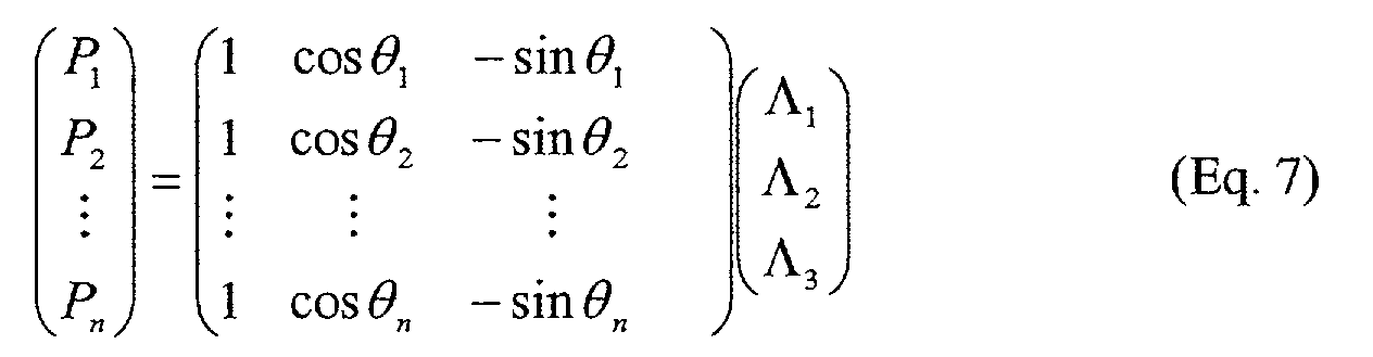
- an analogous analysis can be performed by phase shifting the illuminator 14 instead of the intensifier 26. If an image bundle comprising more than three images is captured, then the estimates of range can be enhanced by a least squares analysis using a singular value decomposition (see, e.g., W.H. Press, B.P. Flannery, S.A. Teukolsky and W.T. Vetterling, Numerical Recipes (the Art of Scientific Computing), Cambridge University Press, Cambridge, 1986).
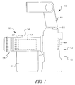
- the first component is an image capture device 40, preferably a single lens reflex (SLR) camera body 42 having an image capture element 44; a typical capture element could be a photosensitive film (which would be used in a range imaging system as described in the aforementioned U.S. Patent No. 6,118,946) or an electronic sensor, such as a charged-coupled-device (CCD).
- SLR single lens reflex
- CCD charged-coupled-device
- the image capture device 40 is able to capture a plurality of range images, i.e., the aforementioned bundle of images.
- the image capture device 40 would include image storage means (not shown) to store all the range images in the image bundle, as well as, e.g., a color texture image in addition to the range images.
- image storage means such as a an internal memory together with output connections to, e.g., a PCMCIA card or a floppy disk (not shown) for receiving images from the internal memory.
- an on-camera storage means such as a an internal memory together with output connections to, e.g., a PCMCIA card or a floppy disk (not shown) for receiving images from the internal memory.
- a means for advancing, or driving, the image capture device 40 to prepare for a successive image capture must be available. Such capabilities are well known in relation to such image capture devices, and will not be described in detail.
- the second component is an illumination device 46 for producing high-frequency amplitude modulated illumination of a desired average amplitude, amplitude modulus and frequency.
- the illumination device 46 is configured as a removable unit 48 that is attached to the camera body 42 via a conventional hot shoe connection 50. It is also desirable that the illumination device 46 includes the capability of shifting the phase of the amplitude modulation between a set of prescribed phase offsets (alternatively, this function may be performed by modulation of the reflected illumination in the optical portion of the scannerless range imaging system). It is also useful for the illumination device 46 to have a preferred operating wavelength, such as in the infrared region of the spectrum.
- the illumination device 46 has the primary purpose of producing amplitude-modulated illumination with its phase controllable for generating a shift in the transmitted wave pattern for each range image in the image bundle (although, as mentioned before, this function may be performed by modulation of the reflected illumination).
- the illumination device 46 includes a light emitting diode (LED) light source and a modulation circuit for generating the requisite modulation signals of predetermined frequency with a set of predetermined phase offsets.
- a controlled angle diffusion sheet such as the Light Shaping Diffuser® from Physical Optics Corporation, is positioned in front of the light source in order to spread the modulated light across the desired field of view as uniformly as possible.
- the illumination device 46 may also include a standard wide-band illumination source that is not modulated.
- This illumination source is used for intensity (non-ranging) photographic images, and may be based on a commonly known and understood flash of a standard camera system, e.g., a commonly available electronic flash of the type useful with photographic cameras.
- the intensity illumination could be provided by separate LEDs, e.g., red, green and blue LEDs, that are chosen so as to provide a white illumination similar to an electronic flash.
- One approach would be to cluster the RGB LEDs in and around each modulated (IR) LED used for ranging. There are many possibilities for such "clustering"; for example, as shown in Figure 11A, an LED cluster could be constituted by one each of RGB and IR LEDs.
- RGB LEDs could be clustered around each IR LED in a hexagonal layout. In either case, the layout shown would be replicated as necessary to provide the needed illumination. Source color temperature could be controlled by the current through each color group. And, whatever the layout, it would be superimposed upon the layouts that will be described for the modulated (IR) LEDs in connection with Figures 9 and 10.
- the illumination device 46 would operate in either of the following modes: a) a first mode in which the light source is operated to illuminate the scene with a plurality (bundle) of exposures, each with a unique phase offset applied to its modulated frequency; and b) a second mode in which the standard wide-band illumination device is operated during capture of an intensity image, e.g., a color texture image. If ambient light is sufficient, of course, it may be unnecessary for the illumination device to operate in the second mode in order to capture an intensity image; in that case, the image capture device would be instructed to operate without flash. Moreover, the sequence of image capture may be reversed, that is, the second mode may be engaged before the first mode or, indeed, the second mode might in specific situations be engaged between the several exposures of the first mode.
- the third component is an optical assembly 52, which includes a lens 54 and a depth capture optical tube 56.
- the optical tube 56 incorporates a modulating element 58, such as the intensifier 26 (see Figure 8), for modulating the incoming reflected scene light that is directed toward the capture element 44 in the camera body 42.
- the optical tube 56 also includes an IR bandpass filter 59 in order to eliminate background illumination, and may incorporate other opto-mechanical elements, such as a shutter 57.
- the optical assembly 52 is shown as a removable optical element that is connected to the image capture device 40 by means of a lens mount 60 on the camera body 42. This is to further emphasize that the image capture device 40 may be based on a conventional camera body that could otherwise be fitted with a standard family of lenses for conventional photography.
- the fourth component is a controller 62, which manages the overall image capture process of the range imaging system, including the operation of the illumination device 46, the image capture device 40, and the optical assembly 52.
- the controller 62 includes the necessary drivers and other circuitry (not shown) for operating the modulating element 58 in proper synchronism with an image capture event.
- the controller 62 could be part of, or attached to, the camera body 42, and the necessary electrical linkages to the optical assembly could be made directly through the camera body 42, e.g., through contacts in the lens mount 60.
- the illumination device 46 comprises three primary assemblies: an illumination section 70, an LED driver stage 72 and a power and control interface 74.
- the illumination device 46 also includes electrical connectors 76 and 78 for an exposure control signal input and a power input, a display and user control section 80 for displaying status indicators and providing one or more switches for on/off and other functions, and a camera mount 82 for attaching the device 46 to the hot shoe connector 50 on the camera body 42.
- the illumination device 46 may be configured in two connected parts 46a and 46b, where the upper part 46a with the illumination section 70 can articulate about a pivot 46c for better aiming, etc.
- the entire illumination device 46 is intended to be a self contained unit that attaches to the hot shoe connector 50 of the camera body 42 via the camera mount 82. This is to further emphasize that the illumination device 46 may be based on a conventional flash body that could be fitted to a standard camera body.
- the illumination section 70 contains a plurality of light emitting diodes (LEDs) 84 mounted onto a heat sink (copper bar) 86, a diffuser plate 88 (preferably a Holographic Light Shaping Diffuser® from Physical Optics Corporation) at the illumination exit port of the illumination section 70, and a thin layer of insulation material 90 (preferably a material identified as Sil-PADTM available from Bergquist Co., Chanhassen, Minnesota) placed between the diodes 84 and the copper heat sink 86 to provide electrical isolation and good thermal conductivity.
- the circuit traces connecting the LEDs are completed on a printed circuit board 91 on the backside of the heat sink 86.
- infrared LEDs are available (e.g.
- part number CLE330E from Clairex Technologies Inc., which have a peak emission at 850 nm.) which can be modulated at frequencies sufficient for depth capture (e.g. 12.5 MHz.).
- High current threshold is not an issue with LEDs, which can provide illumination from a very low current (10's of milliamperes) to a high continuous current (100 milliamperes ) to a very high current ( amperes ) in a pulsed mode.
- the non-coherency property of the LED provides inherent dispersion that can be controlled using simple lenses mounted directly onto the LED at the time of manufacturing.
- Ample illumination is obtained by using multiple LEDs. While only one LED 84 is shown in Figure 3 for clarity of illustration, it should be understood that a plurality of LEDs are mounted through four rows 85 and 87 of hole perforations in the insulation material 90 and the heat sink 86, respectively.
- five LED diodes which are termed an "LED bank” are connected together on the printed circuit board 91 to operate in series; eight banks (i.e., forty LEDs) are contained in the illumination device 46. Grouping the LEDs 84 in this fashion provides a good compromise between the number of driver circuits required and the driver capability. Nonetheless, these numbers of LEDs and banks are not to be seen as limitations, and a greater or fewer number of diodes, or diodes per bank, may be used in other embodiments according to the invention.
- the LED diodes 84 are mounted on the circuit board 90 in a dispersed fashion so that a bank failure would have minimal impact on the distribution of the illumination.
- the LED diodes 84 are mounted in a regular pattern, which is helpful in more easily maintaining uniform trace lengths and thereby avoiding any phase discrepancy between the LED banks.
- rows of LED diodes 84 are arranged using an offset placement pattern to provide more uniform distribution of the output illumination.
- the radiating full angle provides wide and reasonably uniform field illumination, especially at a short distance.
- the diffuser 88 is used to provide an additional but small amount of diffusion (10°) of the LED output; this further enhances uniformity for close field illumination.
- the diffuser material also provides protection for the interior of the illumination compartment, which encases the LED driver circuitry.
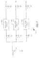
- an LED driver circuit 100 provides controlled current drive for a bank 92 of LEDs 84. Eight of these driver circuits 100 are contained within the LED driver section 72 of the illumination device 46 in order to drive eight banks of LEDs.
- Current through each of the LEDs 84 in the bank 92 is established via the input voltage Vmod x to a first stage amplifier 102.
- the input voltage Vmod x controls the level of illumination generated by the bank of LEDs, i.e., both as to the mean level and the peak to peak modulation.
- a second stage amplifier 104 using the reference voltage Vref, overcomes the offset forward bias needed by the LEDs, which is approximately +8.5Vdc depending upon the diodes chosen and the operating current through the diodes.
- the effective gain on the first stage 102 is approximately 16 depending upon the diodes and trim circuit 112.
- a second amplifier stage 104 By using a second amplifier stage 104, the dynamic range of the first stage is preserved for the range of the amplified output, that is, ⁇ 16 x Vmod x .
- An R-C network 106 provides pole-zero compensation for loop stability and a unity gain buffer amplifier 110 delivers the high current needed to drive the LED bank 92.
- a trim potentiometer P in a current trim circuit 112 provides a limited adjustment in the load resistor R L , such that the LED banks 92 have matching diode radiance for a given input voltage Vmod x .
- a FET switch 108 controls the on/off state of the LED bank 92 in response to an LED On signal derived within the power and control interface circuitry 74.
- the bank 92 is turned on during the exposure period of the camera and gated off otherwise; in this embodiment, the bank 92 is also gated on during camera focus.
- the interface portion of the circuitry 74 establishes the on state of all LED banks 92 in response to a received exposure control signal input to the illumination device 46 through the exposure control signal input connection 76 (see Figure 2).
- This exposure control signal is based on a clock signal generated by the controller 62 (see Figure 1) when the controller references an actual camera exposure signal (the "camera exposure signal” shown in Figures 6A and 6B) generated by the camera body 42 at the beginning of an exposure period.
- the exposure control signal may either be optically coupled through a fiber optic receiver 116 or wire coupled through a coax connector 118. The optical coupling enables control of the light illumination device 46 either locally or remotely while providing good common mode immunity to system noise.
- the exposure control signal is coupled to a signal conditioner and amplifier 120, which functions as a differential receiver, particularly for the differential fiber optic signal, and produces a clock signal 122 (the "received clock signal” shown in Figures 6A and 6B).
- the duration of the exposure control signal is equal to the exposure period with the addition of a 12 ms precursor time interval.
- the precursor time interval is established by firmware within the camera itself. The precursor interval accommodates the initiation of electrical-mechanical operations, such as shutter opening in the depth capture optical tube 56, prior to image exposure.
- the received clock signal 122 is active for the duration of the exposure time established by the camera, as indicated by the camera exposure signal seen in Figures 6A and 6B.
- the received clock signal 122 appears as a 12.5 MHz. clock occurring for the duration of the input exposure control signal. From this clock signal, the interface circuit generates the input modulation signal Vmod x used to drive the eight LED banks 92.
- the input clock signal also performs the following functions: a) it establishes the modulation frequency (e.g.
- the intensifier modulation signal shown in Figures 6A and 6B is the modulation signal applied to the intensifier 26 shown in Figure 8.
- the clock signal 122 is filtered through a resonant LC filter 124 and produces a sinusoidal output voltage 126.
- the sinusoidal signal 126 when added in a summing amplifier 128 to a selected dc offset voltage V op becomes the controlling voltage for the LED bank 92, i.e. the voltage signal Vmod x .
- the level of LED illumination follows Vmod x , both in amplitude and phase.
- the input clock phase of Vmod x is shifted with respect to the phase of the intensifier modulation in accordance with preset phase increment values, as explained in connection with Figure 8.
- FIG. 6B shows the phase of input voltage signal Vmod x for the second frame shifted by t 2 relative to the first frame shown in Figure 6A.
- the interface circuitry 74 activates the LED bank 92 only when the transmitted modulation signal is sufficiently present.
- a detection circuit 132 monitors the received clock signal 122. If the received clock signal 122 is present for more than a predetermined time period (e.g., 1.28 ⁇ s or 16 clock cycles), the detection circuit 132 generates the LED On signal and the LED drive current is activated (see Figure 4); if the received clock signal 122 is absent for a predetermined time (e.g., 0.16 ⁇ s or 2 clock cycles), the detection circuit 132 disables the LED On signal and the LED drive current is deactivated.
- the detection circuit can take a variety of conventional forms, such as a logical counter, an R-C network with a comparator, or one-shot circuitry, depending upon the precision needed.
- the power and control interface circuitry 74 includes power conditioning circuitry 140, which receives an external supply (e.g., +18Vdc) through the power input connector 78. Then, through the use of internal regulators 142a, 142b and 142c, the power conditioning circuitry 140 establishes the +/- dc supplies (e.g., +V s , -V s , +V c ) needed for the other circuitry in the illumination circuit 46. Levels for the three supplies are typically +15Vdc, -15Vdc, +5Vdc, respectively. Since the supply regulation is conventional, the particular designs for conditioning and regulation of the supplies are readily understood by one of ordinary skill in this art and will not be further described.
- an external supply e.g., +18Vdc
- the power conditioning circuitry 140 establishes the +/- dc supplies (e.g., +V s , -V s , +V c ) needed for the other circuitry in the illumination circuit 46.
Landscapes
- Engineering & Computer Science (AREA)
- Physics & Mathematics (AREA)
- Computer Networks & Wireless Communication (AREA)
- General Physics & Mathematics (AREA)
- Radar, Positioning & Navigation (AREA)
- Remote Sensing (AREA)
- Electromagnetism (AREA)
- Studio Devices (AREA)
- Length Measuring Devices By Optical Means (AREA)
- Circuit Arrangement For Electric Light Sources In General (AREA)
- Optical Radar Systems And Details Thereof (AREA)
- Facsimile Scanning Arrangements (AREA)
Abstract
Description

Claims (6)
- A light emitting diode (LED) illumination device for generating modulated light for a scannerless range imaging system, said illumination device comprising:circuitry for generating a drive signal having given phase and frequency characteristics;a plurality of light emitting diodes arranged in a plurality of LED banks, wherein each LED bank comprises a plurality of light emitting diodes connected in series to the circuitry to receive the drive signal; anda switching stage for simultaneously activating the plurality of LED banks such that the LED banks generate the modulated light according to the phase and frequency characteristics of the drive signal.
- The illumination device as claimed in claim 1 wherein the plurality of LED banks are arranged on a circuit board in a dispersed fashion such that a bank failure would have minimal impact on the distribution of the illumination.
- The illumination device as claimed in claim 1 wherein the plurality of LED banks are arranged on a circuit board with the light emitting diodes in a offset placement pattern to provide a more uniform distribution of the output illumination.
- The illumination device as claimed in claim 1 wherein the light emitting diodes have a peak emission in the infrared region of the spectrum.
- A light emitting diode (LED) illumination device for generating modulated light for a scannerless range imaging system in response to an exposure control signal, said illumination device comprising:an interface circuit for generating a modulating signal in response to the exposure control signal, said modulating signal having given phase and frequency characteristics;a plurality of drive circuits for generating a plurality of drive signals from the modulating signal, whereby each drive signal has the given phase and frequency characteristics; anda plurality of light emitting diodes arranged in a plurality of LED banks, wherein each LED bank comprises a smaller plurality of light emitting diodes connected in series to a given one of the drive circuits to generate the modulated light according to the phase and frequency characteristics of the modulating signal.
- The illumination device as claimed in claim 5 further comprising a switching stage responsive to the exposure control signal for activating the plurality of drive circuits, thereby activating the plurality of LED banks such that they generate the modulated light according to the phase and frequency characteristics of the modulating signal.
Applications Claiming Priority (2)
| Application Number | Priority Date | Filing Date | Title |
|---|---|---|---|
| US776286 | 2001-02-02 | ||
| US09/776,286 US6584283B2 (en) | 2001-02-02 | 2001-02-02 | LED illumination device for a scannerless range imaging system |
Publications (2)
| Publication Number | Publication Date |
|---|---|
| EP1229349A2 true EP1229349A2 (en) | 2002-08-07 |
| EP1229349A3 EP1229349A3 (en) | 2003-04-23 |
Family
ID=25106964
Family Applications (1)
| Application Number | Title | Priority Date | Filing Date |
|---|---|---|---|
| EP02075242A Withdrawn EP1229349A3 (en) | 2001-02-02 | 2002-01-21 | Led illumination device for a scannerless range imaging system |
Country Status (4)
| Country | Link |
|---|---|
| US (1) | US6584283B2 (en) |
| EP (1) | EP1229349A3 (en) |
| JP (1) | JP2002323302A (en) |
| IL (1) | IL147028A0 (en) |
Cited By (1)
| Publication number | Priority date | Publication date | Assignee | Title |
|---|---|---|---|---|
| WO2013026679A1 (en) * | 2011-08-25 | 2013-02-28 | Ifm Electronic Gmbh | Time-of-flight camera with signal path monitoring |
Families Citing this family (45)
| Publication number | Priority date | Publication date | Assignee | Title |
|---|---|---|---|---|
| US20050174473A1 (en) * | 1999-11-18 | 2005-08-11 | Color Kinetics, Inc. | Photography methods and systems |
| JP4288553B2 (en) | 2000-07-25 | 2009-07-01 | 富士フイルム株式会社 | Camera strobe device |
| FI111417B (en) * | 2001-06-01 | 2003-07-15 | Nokia Corp | Control of flash light in a digital camera |
| US6707054B2 (en) * | 2002-03-21 | 2004-03-16 | Eastman Kodak Company | Scannerless range imaging system having high dynamic range |
| JP2004071807A (en) * | 2002-08-06 | 2004-03-04 | Sharp Corp | Lighting device, camera device, and portable device |
| WO2005012997A2 (en) * | 2003-07-25 | 2005-02-10 | Color Kinetics, Inc. | Photography methods and systems |
| JP4227491B2 (en) * | 2003-09-09 | 2009-02-18 | 株式会社リコー | Power supply circuit for digital camera |
| JP4542773B2 (en) * | 2003-12-22 | 2010-09-15 | Hoya株式会社 | Lighting control device |
| US7643084B2 (en) * | 2003-12-22 | 2010-01-05 | Hoya Corporation | Lighting control apparatus |
| JP4495448B2 (en) * | 2003-12-22 | 2010-07-07 | Hoya株式会社 | Lighting control device |
| US20050243302A1 (en) * | 2004-01-20 | 2005-11-03 | Bedabrata Pain | Two dimensional range-imaging |
| JP2006337286A (en) * | 2005-06-03 | 2006-12-14 | Ricoh Co Ltd | Shape measuring device |
| TWI391600B (en) * | 2005-09-27 | 2013-04-01 | Koninkl Philips Electronics Nv | Led lighting fixtures |
| US20070225778A1 (en) * | 2006-03-23 | 2007-09-27 | Heacock Gregory L | PDT apparatus with an addressable LED array for therapy and aiming |
| JP5124864B2 (en) * | 2006-06-07 | 2013-01-23 | 本田技研工業株式会社 | Optical device and moving device |
| US7995191B1 (en) * | 2006-06-29 | 2011-08-09 | Sandia Corporation | Scannerless laser range imaging using loss modulation |
| US7495748B1 (en) * | 2007-08-20 | 2009-02-24 | Sandia Corporation | Scannerless loss modulated flash color range imaging |
| US7420656B1 (en) * | 2007-08-20 | 2008-09-02 | Sandia Corporation | Scannerless loss modulated flash color range imaging |
| CN101453659B (en) * | 2007-12-04 | 2010-12-29 | 深圳Tcl新技术有限公司 | Lighting system and its method of operation in a video display unit |
| CN101453620A (en) * | 2007-12-04 | 2009-06-10 | 深圳Tcl新技术有限公司 | Method and electronic device for providing popular program |
| CN101452192B (en) * | 2007-12-04 | 2010-09-08 | 深圳Tcl新技术有限公司 | Lighting system and its method of operation in a video display unit |
| CN101451674B (en) * | 2007-12-04 | 2011-01-19 | 深圳Tcl新技术有限公司 | Lighting system and operation mode thereof in video display unit |
| CN101469829A (en) * | 2007-12-25 | 2009-07-01 | 深圳Tcl新技术有限公司 | Illuminating system and operation method thereof |
| CN101498404A (en) * | 2008-02-03 | 2009-08-05 | 深圳Tcl新技术有限公司 | Illuminating system, operation method thereof in video display unit |
| US8497478B2 (en) * | 2009-03-31 | 2013-07-30 | Osram Sylvania Inc. | High voltage supply to increase rise time of current through light source in an optical sensor system |
| US8194149B2 (en) * | 2009-06-30 | 2012-06-05 | Cisco Technology, Inc. | Infrared-aided depth estimation |
| KR101648353B1 (en) * | 2009-09-25 | 2016-08-17 | 삼성전자 주식회사 | Image sensor having depth sensor |
| JP5338773B2 (en) * | 2010-08-26 | 2013-11-13 | パナソニック株式会社 | Component mounting apparatus, imaging illumination apparatus, and illumination method |
| EP2667218B1 (en) * | 2010-11-15 | 2017-10-18 | Cedes AG | Energy efficient 3D sensor |
| US9697588B2 (en) | 2010-11-15 | 2017-07-04 | Intuitive Surgical Operations, Inc. | System and method for multi-resolution sharpness transport across color channels |
| DE102011078307A1 (en) * | 2011-06-29 | 2013-01-03 | Ifm Electronic Gmbh | Lighting for a light runtime camera |
| GB2492833A (en) * | 2011-07-14 | 2013-01-16 | Softkinetic Sensors Nv | LED boost converter driver circuit for Time Of Flight light sources |
| KR20130101836A (en) * | 2012-03-06 | 2013-09-16 | 삼성전자주식회사 | Lighting device and photographing system including the same |
| EP2842330B1 (en) | 2012-04-13 | 2018-08-29 | Red.Com, Llc | Video projector system |
| US9025086B2 (en) | 2012-04-13 | 2015-05-05 | Red.Com, Inc. | Video projector system |
| US9071763B1 (en) | 2012-09-26 | 2015-06-30 | Google Inc. | Uniform illumination image capture |
| WO2014178047A1 (en) | 2013-04-30 | 2014-11-06 | Inuitive Ltd. | System and method for video conferencing |
| JP2016031291A (en) * | 2014-07-29 | 2016-03-07 | Fdk株式会社 | Optical sensor module, power storage module, and distance measuring method |
| US11428786B2 (en) | 2017-12-03 | 2022-08-30 | Munro Design & Technologies, Llc | Dual waveforms for three-dimensional imaging systems and methods thereof |
| US10721393B2 (en) * | 2017-12-29 | 2020-07-21 | Axis Ab | Laser ranging and illumination |
| DE102018203352B4 (en) * | 2018-03-07 | 2026-02-05 | Robert Bosch Gmbh | Transmitter unit and LIDAR device for scanning a scanning area |
| CN113545169B (en) * | 2019-01-14 | 2025-04-22 | 亮锐控股有限公司 | Lighting equipment for FM transmission |
| CN111178108B (en) * | 2020-01-21 | 2025-04-25 | 东莞华贝电子科技有限公司 | Scanning module and data collection terminal |
| US11579449B2 (en) * | 2020-05-29 | 2023-02-14 | Microsoft Technology Licensing, Llc | Systems and methods for providing mixed-reality experiences under low light conditions |
| US12376208B2 (en) | 2023-06-16 | 2025-07-29 | Omron Corporation | Controlling energy efficiency in LED drive circuits |
Family Cites Families (7)
| Publication number | Priority date | Publication date | Assignee | Title |
|---|---|---|---|---|
| US4891624A (en) | 1987-06-12 | 1990-01-02 | Stanley Electric Co., Ltd. | Rearward vehicle obstruction detector using modulated light from the brake light elements |
| US4935616A (en) | 1989-08-14 | 1990-06-19 | The United States Of America As Represented By The Department Of Energy | Range imaging laser radar |
| US6088086A (en) | 1995-09-11 | 2000-07-11 | Sandia Corporation | Range determination for scannerless imaging |
| US5877851A (en) * | 1997-09-24 | 1999-03-02 | The United States Of America As Represented By The Secretary Of The Army | Scannerless ladar architecture employing focal plane detector arrays and FM-CW ranging theory |
| US6876392B1 (en) | 1998-12-22 | 2005-04-05 | Matsushita Electric Industrial Co., Ltd. | Rangefinder for obtaining information from a three-dimensional object |
| WO2000049332A1 (en) | 1999-02-16 | 2000-08-24 | Tokheim Corporation | Led backlighting apparatus for use in fuel dispensers |
| US6118946A (en) | 1999-06-29 | 2000-09-12 | Eastman Kodak Company | Method and apparatus for scannerless range image capture using photographic film |
-
2001
- 2001-02-02 US US09/776,286 patent/US6584283B2/en not_active Expired - Lifetime
- 2001-12-11 IL IL14702801A patent/IL147028A0/en unknown
-
2002
- 2002-01-21 EP EP02075242A patent/EP1229349A3/en not_active Withdrawn
- 2002-02-01 JP JP2002026047A patent/JP2002323302A/en active Pending
Cited By (3)
| Publication number | Priority date | Publication date | Assignee | Title |
|---|---|---|---|---|
| WO2013026679A1 (en) * | 2011-08-25 | 2013-02-28 | Ifm Electronic Gmbh | Time-of-flight camera with signal path monitoring |
| CN103608695A (en) * | 2011-08-25 | 2014-02-26 | Ifm电子股份有限公司 | Time-of-flight camera with signal path monitoring |
| CN103608695B (en) * | 2011-08-25 | 2016-01-20 | Ifm电子股份有限公司 | There is the time-of-flight camera of signal path monitoring |
Also Published As
| Publication number | Publication date |
|---|---|
| US20020172514A1 (en) | 2002-11-21 |
| JP2002323302A (en) | 2002-11-08 |
| US6584283B2 (en) | 2003-06-24 |
| IL147028A0 (en) | 2002-08-14 |
| EP1229349A3 (en) | 2003-04-23 |
Similar Documents
| Publication | Publication Date | Title |
|---|---|---|
| US6584283B2 (en) | LED illumination device for a scannerless range imaging system | |
| US20030147002A1 (en) | Method and apparatus for a color sequential scannerless range imaging system | |
| US5903996A (en) | Day/night viewing device with laser range finder utilizing two wavelengths of laser light, and method of its operation | |
| US5870180A (en) | Time measurement device and method useful in a laser range camera | |
| US6707054B2 (en) | Scannerless range imaging system having high dynamic range | |
| US7119842B2 (en) | Image capturing device including a spectrally-selectively transmissive diaphragm | |
| US7319557B2 (en) | Fused thermal and direct view aiming sight | |
| US9451240B2 (en) | 3-dimensional image acquisition apparatus and 3D image acquisition method for simultaneously obtaining color image and depth image | |
| EP1178333A2 (en) | Method and apparatus for a color scannerless range imaging system | |
| JP2938912B2 (en) | Imaging Rider System | |
| EP3401631B1 (en) | Thermal reflex sight | |
| US4642452A (en) | Semiactive night viewing system | |
| US6507706B1 (en) | Color scannerless range imaging system using an electromechanical grating | |
| US6349174B1 (en) | Method and apparatus for a color scannerless range imaging system | |
| US5434612A (en) | Duo-frame normalization technique | |
| EP3543742B1 (en) | A 3d imaging system and method of 3d imaging | |
| Gerken et al. | Military reconnaissance platform for the spectral range from the visible to the MWIR | |
| US11172108B2 (en) | Imaging device | |
| US20200252535A1 (en) | Heterodyne starring array active imager with spread spectrum illuminator | |
| WO2006090356A1 (en) | Add-on laser gated imaging device for associating with an optical assembly | |
| JPH07318814A (en) | Microphotographic device | |
| CN101681777A (en) | System for artificially enhancing image display contrast | |
| Stann et al. | Chirped amplitude modulation ladar for range and Doppler measurements and 3-D imaging | |
| US10587347B1 (en) | Heterodyne starring array active imager | |
| KR102926361B1 (en) | Active imaging system |
Legal Events
| Date | Code | Title | Description |
|---|---|---|---|
| PUAI | Public reference made under article 153(3) epc to a published international application that has entered the european phase |
Free format text: ORIGINAL CODE: 0009012 |
|
| AK | Designated contracting states |
Kind code of ref document: A2 Designated state(s): AT BE CH CY DE DK ES FI FR GB GR IE IT LI LU MC NL PT SE TR |
|
| AX | Request for extension of the european patent |
Free format text: AL;LT;LV;MK;RO;SI |
|
| PUAL | Search report despatched |
Free format text: ORIGINAL CODE: 0009013 |
|
| AK | Designated contracting states |
Designated state(s): AT BE CH CY DE DK ES FI FR GB GR IE IT LI LU MC NL PT SE TR |
|
| AX | Request for extension of the european patent |
Extension state: AL LT LV MK RO SI |
|
| RIC1 | Information provided on ipc code assigned before grant |
Ipc: 7G 03B 7/00 B Ipc: 7G 01S 17/32 B Ipc: 7G 01S 17/87 B Ipc: 7G 01S 7/491 B Ipc: 7G 01S 17/89 A |
|
| AKX | Designation fees paid | ||
| REG | Reference to a national code |
Ref country code: DE Ref legal event code: 8566 |
|
| STAA | Information on the status of an ep patent application or granted ep patent |
Free format text: STATUS: THE APPLICATION IS DEEMED TO BE WITHDRAWN |
|
| 18D | Application deemed to be withdrawn |
Effective date: 20031024 |