EP1227664A1 - Photosensor array using segmented charge transfer gates to improve processing time for small images - Google Patents
Photosensor array using segmented charge transfer gates to improve processing time for small images Download PDFInfo
- Publication number
- EP1227664A1 EP1227664A1 EP02250341A EP02250341A EP1227664A1 EP 1227664 A1 EP1227664 A1 EP 1227664A1 EP 02250341 A EP02250341 A EP 02250341A EP 02250341 A EP02250341 A EP 02250341A EP 1227664 A1 EP1227664 A1 EP 1227664A1
- Authority
- EP
- European Patent Office
- Prior art keywords
- charges
- photosensors
- charge
- shift register
- charge transfer
- Prior art date
- Legal status (The legal status is an assumption and is not a legal conclusion. Google has not performed a legal analysis and makes no representation as to the accuracy of the status listed.)
- Withdrawn
Links
Images


Classifications
-
- H—ELECTRICITY
- H04—ELECTRIC COMMUNICATION TECHNIQUE
- H04N—PICTORIAL COMMUNICATION, e.g. TELEVISION
- H04N25/00—Circuitry of solid-state image sensors [SSIS]; Control thereof
- H04N25/70—SSIS architectures; Circuits associated therewith
- H04N25/701—Line sensors
-
- H—ELECTRICITY
- H04—ELECTRIC COMMUNICATION TECHNIQUE
- H04N—PICTORIAL COMMUNICATION, e.g. TELEVISION
- H04N25/00—Circuitry of solid-state image sensors [SSIS]; Control thereof
- H04N25/40—Extracting pixel data from image sensors by controlling scanning circuits, e.g. by modifying the number of pixels sampled or to be sampled
- H04N25/44—Extracting pixel data from image sensors by controlling scanning circuits, e.g. by modifying the number of pixels sampled or to be sampled by partially reading an SSIS array
- H04N25/443—Extracting pixel data from image sensors by controlling scanning circuits, e.g. by modifying the number of pixels sampled or to be sampled by partially reading an SSIS array by reading pixels from selected two-dimensional [2D] regions of the array, e.g. for windowing or digital zooming
Definitions
- This invention relates generally to photosensor arrays used for optical image scanners and cameras, and more specifically to line arrays commonly used for optical image scanners.
- Image scanners convert a visible image on a document or photograph, or an image in a transparent medium, into an electronic form suitable for copying, storing or processing by a computer.
- An image scanner may be a separate device or an image scanner may be a part of a copier, part of a facsimile machine, or part of a multipurpose device.
- Reflective image scanners typically have a controlled source of light, and light is reflected off the surface of a document, through an optics system, and onto an array of photosensitive devices. The photosensitive devices convert received light intensity into an electronic signal.
- Transparency image scanners pass light through a transparent image, for example a photographic positive slide, through an optics system, and then onto an array of photosensitive devices.
- image scanners use an optical lens system to focus an image onto an array of photosensors.
- the line array in conjunction with the scanner optics system, defines a scanline on the document being scanned.
- Photosensor arrays typically have thousands of individual photosensitive elements. Each photosensitive element, in conjunction with the scanner optics system, measures light intensity from an effective area on the document defining a picture element (pixel) on the image being scanned.
- CCD Charge Coupled Devices
- CID Charge Injection Devices
- CMOS Complementary-Metal-Oxide
- solar cells typically, for a CID or a CMOS array, each photosensitive element is addressable.
- CCD line arrays commonly serially transfer all the charges, bucket-brigade style, from each line array of photosensitive elements to a small number of sense nodes for conversion of charge into a measurable voltage.
- serial charge shift registers also called charge transfer registers or serial readout registers.
- a document, or photograph, or other image being scanned is substantially smaller than the maximum size that the scanner is capable of scanning.
- a scanner capable of scanning a document that is about 220 mm wide may be used to scan a film negative or slide that is about 35 mm wide.
- a scanner capable of scanning U.S. "B" size documents or Metric A3 documents may also routinely be used to scan U.S. "A” size documents or Metric A4 documents.
- scanners commonly provide a preview function, where an entire page is scanned at a low resolution, and a scanner operator then selects a small portion of the page for a final scan at high resolution.
- the scanner converts charges to digital values for the maximum number of pixels in a scanline, and then discards the unwanted digital values. A substantial amount of time is spent generating digital data that is never used. For high-resolution scanning of small images or small portions of a page, scanning speed may be limited by conversion of data that is never used. There is a need for decreasing the time required for scanning an area having a width that is relatively small compared to the maximum scan width for a scanner.
- a photosensor assembly has charge transfer gates that are segmented into multiple sections. Individual sections can be controlled. For a small image, only the appropriate sections of the charge transfer gates are used to transfer charges from the photosensors to charge shift registers. The charge shift registers shift the charges toward a node for analog-to-digital conversion. When all the charges have been shifted beyond the appropriate sections of the charge transfer gates, the appropriate sections of the charge transfer gates can be activated again. As a result, multiple partial scanlines may be multiplexed onto the charge shift register. In the steady state, only the charges from a small section of the image are converted, thereby reducing processing time. If overall scanning time is limited by exposure time, then the shift rate can be decreased as a result of shifting fewer charges, thereby improving charge transfer efficiency. Accumulated charges in photosensors that are not being used are drained into overflow drains.
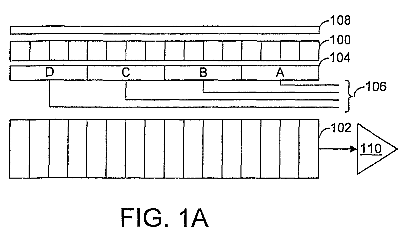
- a photosensor assembly includes a line array of photosensors 100, and a charge shift register 102.
- a charge transfer gate 104 is segmented into multiple sections. As depicted in the example of figure 1A, the charge transfer gate 104 is segmented into four equal-length sections, labeled A, B, C, and D, with each section separately controllable by control lines 106. After exposure, control of the sections of the charge transfer gate 104 determines which charges from the line array of photosensors are transferred to the charge shift register 102. For example, all four sections of the charge transfer gate 104 may be activated, so that the maximum width scanline is captured, or half the width may be captured, or any other combination of fourths.
- a lateral overflow drain 108 prevents excess charge from accumulating.
- charges in the charge shift register 102 are shifted to an amplifier 110 for analog-to-digital conversion (A/D converter not illustrated).
- processing time (which consists of shift time and A/D conversion time) is reduced to about one-fourth of the processing time required for full width scanlines.
- processing time is reduced to about one-fourth of the processing time required for full width scanline, regardless of which section of the charge transfer gate is used.
- the only variable is how many partial scanlines are multiplexed. For example, if only section A of the charge shift register is used, then processing time is reduced by about a factor of four, with no multiplexing. If only section B of the charge shift register is used, then processing time is reduced by about a factor of four, with two partial scanlines multiplexed.
- CTE Charge Transfer Efficiency
- TTE Total Transfer Efficiency
- segmented charge transfer gates With segmented charge transfer gates, fewer charges are processed during the next exposure time, so the clock rate for the charge transfer gate can be decreased, thereby improving CTE and TTE.
- both benefits may be obtained. For example, in a hypothetical scanner, assume that for full width scans the processing time for each scanline is twice the exposure time. Use of a four-segment charge transfer gate can reduce processing time by a factor of four, thereby making the exposure time twice the processing time. The shift rate can then be reduced by a factor of two, making processing time and exposure time equal, with the end result that scanning time is improved by a factor of two, and CTE and TTE are also improved.
- FIG. 2 illustrates use of bilinear readout with segmented charge transfer gates in accordance with the invention.
- a line array 200 transfers charges, through a first charge transfer gate 202, to a first charge shift register 204, and through a second charge transfer gate 208, to a second charge shift register 210.
- Charge shift register 204 shifts charges to amplifier 206
- charge shift register 210 shifts charges to amplifier 212.
- charge transfer gates 202 and 210 are segmented into four equal-length sections. As depicted in figure 2, one-fourth of the charges in line array 200 are transferred to charge shift registers 204 and 210. Within each charge shift register, there is a block of charges (214, 216) that can be multiplexed with charges from successive scanlines. In the example of figure 2, if one-fourth of the charges are transferred, in the steady state after transferred charges reach the amplifiers, one-fourth of the charges in the charge shift registers are being processed while the next scanline is being exposed. Therefore, processing time is reduced to about one-fourth of the processing time required for full width scanlines. Note that in the configuration illustrated in figure 2, there is no room for lateral overflow drains adjacent to the photosensor line array. Accordingly, vertical overflow drains may be implemented beneath the photosensor line array.
- FIG. 3A and 3B illustrate an alternative configuration, with staggered CCD arrays, in which rows of photosensors from two different staggered line arrays share a charge shift register. Sharing a charge shift register is the subject of a separate patent application. However, the configuration in figures 3A and 3B also includes segmented charge transfer gates in accordance with the invention.
- Photosensor row 300 is staggered relative to photosensor row 304.
- Two additional rows of photosensors (312 and 316) share a lateral overflow drain 314.
- Photosensor row 312 is staggered relative to photosensor row 316.
- Photosensor rows 304 and 312 share a charge shift register 308.
- Charge shift registers for photosensor rows 300 and 316 are not illustrated.
- Photosensor row 304 transfers charges, through a charge transfer gate 306, to the charge shift register 308.
- Photosensor row 312 transfers charges, through a charge transfer gate 310, to the charge shift register 308.
- charge transfer gates 306 and 310 are divided into four equal-length sections. Charges in the charge shift register 308 are shifted to an amplifier 318.
- the charge shift register 308 is used twice for each exposure.
- photosensor row 304 may transfer a block of charges to the charge shift register 308 first.
- photosensor row 312 may transfer a block of charges to the charge shift register 308.
- the charges from photosensor rows 304 and 312 may be multiplexed.
- Figures 4A and 4B illustrate example configurations in which segmented charge transfer gates have sections with unequal lengths.
- a row of photosensors 400 transfers charges, through a charge transfer gate 402, to a charge shift register 404. Excess charges from the photosensors are drained to an overflow drain 408.
- the charge transfer gate 402 is divided in two sections, labeled A and B. Section A is longer than section B.
- a specific example is a scanner capable of scanning U.S. "B" size documents or metric A3 documents, where the scanner is also routinely used to scan U.S. "A" size documents or metric A4 documents.
- section A may correspond to a partial-width scanline having a width of about 8.5 inches (U.S.
- Sections A plus B combined may correspond to a full-width scanline having a width of about 11.0 inches (U.S. size "B”), or about 297 mm (metric size A3).
- narrow documents U.S. "A” or metric A4 are placed so that resulting charges are transferred by section A of the charge transfer gate 402.
- both sections A and B of the charge transfer gate 402 are enabled.
- Figure 4B has the same overall configuration as figure 4A, except the charge transfer gate is segmented into three sections, labeled A, B, and C. Section B is smaller than sections A and C, and section B is located near the center of the overall scanline.
- a specific example is a scanner capable of scanning full width documents, but is also used to scan 35 mm slides or film negatives.
- Some light sources commonly used in optical image scanners, for example fluorescent lamps, are brighter near the center of the lamp than at the ends of the lamps. Accordingly, for such lamps, it is preferable to place slides or other small images near the center of the illumination.
- section B of the charge transfer gate 410 is located near the center of the charge transfer gate.
- processing times are compared for: (1) conventional photosensor assemblies without segmented charge transfer gates, and with normal shifting speeds; (2) rapid-shift, and (3) use of segmented charge transfer gates.
- N number of photosensors per row
- T s time to shift from one stage of the charge shift register to the next stage
- T c analog-to-digital conversion time for one voltage measurement, including some signal settling time.
- charges are transferred once in parallel, and then shifted and converted serially. Given a large number of pixels, the one charge transfer time is relatively insignificant compared to total shift time and total A/D conversion time.
- the total time required to process one scanline in conventional configurations is then approximately N*(T S + T C ). If N increases, and all other parameters remain constant, then the time required to process each scanline increases. Typically, one scanline is being exposed while the previous scan line is being converted.
- processing time is cut in half to 2.0 msec, because of the parallel charge shift registers and parallel analog-to-digital conversion.
- total processing time relative to conventional processing is cut in half to 0.875 msec.
- charge transfer gates can be divided into equal-length sections, or non-equal-length sections, with each section separately controllable.
- segmented charge transfer gates enable a decreased scanning time for small partial scanlines within longer scanlines, and improved signal accuracy (improved charge transfer efficiency).
- processing time can be reduced to 1/M times the conventional processing time.
- the location of the image within the charge shift register affects how many partial scanlines are multiplexed, but not the steady state processing time.
Landscapes
- Engineering & Computer Science (AREA)
- Multimedia (AREA)
- Signal Processing (AREA)
- Facsimile Heads (AREA)
- Solid State Image Pick-Up Elements (AREA)
- Automatic Focus Adjustment (AREA)
- Transforming Light Signals Into Electric Signals (AREA)
- Facsimile Scanning Arrangements (AREA)
Abstract
Description
- This invention relates generally to photosensor arrays used for optical image scanners and cameras, and more specifically to line arrays commonly used for optical image scanners.
- Image scanners convert a visible image on a document or photograph, or an image in a transparent medium, into an electronic form suitable for copying, storing or processing by a computer. An image scanner may be a separate device or an image scanner may be a part of a copier, part of a facsimile machine, or part of a multipurpose device. Reflective image scanners typically have a controlled source of light, and light is reflected off the surface of a document, through an optics system, and onto an array of photosensitive devices. The photosensitive devices convert received light intensity into an electronic signal. Transparency image scanners pass light through a transparent image, for example a photographic positive slide, through an optics system, and then onto an array of photosensitive devices.
- In general, image scanners use an optical lens system to focus an image onto an array of photosensors. For line arrays of photosensors, the line array, in conjunction with the scanner optics system, defines a scanline on the document being scanned. Photosensor arrays typically have thousands of individual photosensitive elements. Each photosensitive element, in conjunction with the scanner optics system, measures light intensity from an effective area on the document defining a picture element (pixel) on the image being scanned.
- Common photosensor technologies include Charge Coupled Devices (CCD), Charge Injection Devices (CID), Complementary-Metal-Oxide (CMOS) devices, and solar cells. Typically, for a CID or a CMOS array, each photosensitive element is addressable. In contrast, CCD line arrays commonly serially transfer all the charges, bucket-brigade style, from each line array of photosensitive elements to a small number of sense nodes for conversion of charge into a measurable voltage. The present patent document is primarily concerned with photosensor arrays having serial charge shift registers, also called charge transfer registers or serial readout registers.
- Sometimes, a document, or photograph, or other image being scanned, is substantially smaller than the maximum size that the scanner is capable of scanning. For example, a scanner capable of scanning a document that is about 220 mm wide may be used to scan a film negative or slide that is about 35 mm wide. Alternatively, a scanner capable of scanning U.S. "B" size documents or Metric A3 documents, may also routinely be used to scan U.S. "A" size documents or Metric A4 documents. Finally, scanners commonly provide a preview function, where an entire page is scanned at a low resolution, and a scanner operator then selects a small portion of the page for a final scan at high resolution.
- Typically, the scanner converts charges to digital values for the maximum number of pixels in a scanline, and then discards the unwanted digital values. A substantial amount of time is spent generating digital data that is never used. For high-resolution scanning of small images or small portions of a page, scanning speed may be limited by conversion of data that is never used. There is a need for decreasing the time required for scanning an area having a width that is relatively small compared to the maximum scan width for a scanner.
- A photosensor assembly has charge transfer gates that are segmented into multiple sections. Individual sections can be controlled. For a small image, only the appropriate sections of the charge transfer gates are used to transfer charges from the photosensors to charge shift registers. The charge shift registers shift the charges toward a node for analog-to-digital conversion. When all the charges have been shifted beyond the appropriate sections of the charge transfer gates, the appropriate sections of the charge transfer gates can be activated again. As a result, multiple partial scanlines may be multiplexed onto the charge shift register. In the steady state, only the charges from a small section of the image are converted, thereby reducing processing time. If overall scanning time is limited by exposure time, then the shift rate can be decreased as a result of shifting fewer charges, thereby improving charge transfer efficiency. Accumulated charges in photosensors that are not being used are drained into overflow drains.
-
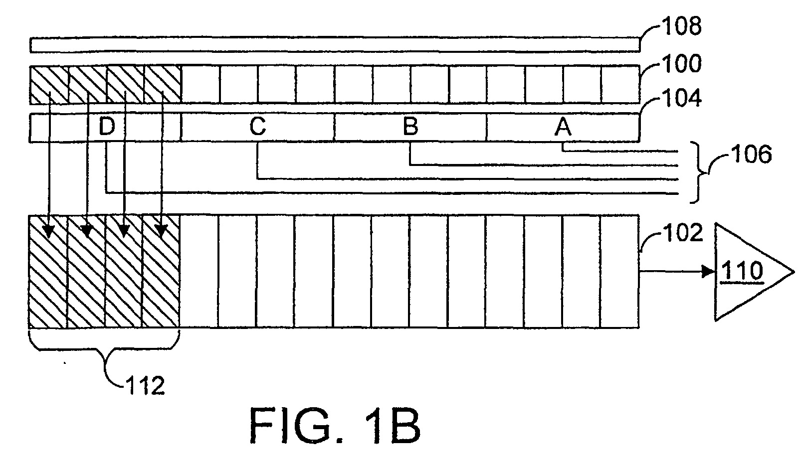
- Figures 1A - 1C are block diagrams of a photosensor assembly with a segmented charge transfer gate in accordance with the invention.
- Figure 2 is a block diagram of an alternative configuration for a photosensor assembly in accordance with the invention.
- Figure 3A and 3B are block diagrams of an additional alternative configuration for a photosensor assembly in accordance with the invention.
- Figures 4A and 4B are block diagrams of additional alternative configurations for segmented charge transfer gates in accordance with the invention.
-
- In figure 1A, a photosensor assembly includes a line array of
photosensors 100, and acharge shift register 102. Acharge transfer gate 104 is segmented into multiple sections. As depicted in the example of figure 1A, thecharge transfer gate 104 is segmented into four equal-length sections, labeled A, B, C, and D, with each section separately controllable bycontrol lines 106. After exposure, control of the sections of thecharge transfer gate 104 determines which charges from the line array of photosensors are transferred to thecharge shift register 102. For example, all four sections of thecharge transfer gate 104 may be activated, so that the maximum width scanline is captured, or half the width may be captured, or any other combination of fourths. With repeated exposures, photosensors having charge that is not transferred will saturate, and charge may overflow to adjacent photosensors. In figure 1A, alateral overflow drain 108 prevents excess charge from accumulating. In figure 1A, charges in thecharge shift register 102 are shifted to anamplifier 110 for analog-to-digital conversion (A/D converter not illustrated). - Assume that only one-fourth of the available scanline width is actually needed. In figure 1B, only one section (section D) of the
charge transfer gate 104 is activated, and a block of charges comprising one-fourth of the charges (112) from theline array 100 are transferred to thecharge shift register 102. The remaining stages in the charge shift register are not affected by this transfer, and are discussed in more detail below. Thecharge shift register 102 shifts thecharges 112 to theamplifier 110 for A/D conversion. - In figure 1C, during a second exposure, charges in the
charge shift register 102 are shifted toward theamplifier 110. After four shifts, thecharge shift register 102 is ready to receive another block of charges from theline array 100. One section (section D) of the charge shift register is again activated, and a block ofcharges 114 comprising one-fourth of the charges from thephotosensor array 100 are transferred to thecharge shift register 102. As discussed above, accumulated charges in the remainder of thephotosensor array 100 are drained to theoverflow drain 108. Note that charges from two different exposures are now multiplexed into thecharge shift register 102. In the example illustrated in figure 1C, if the image of interest is in the charge shift register stages that are the greatest distance from the amplifier, then four partial scanlines, from a small image contained in the one-fourth scanline being captured, can be multiplexed onto thecharge shift register 102. - Once charges that are transferred into the
charge shift register 102 reach the end closest to the amplifier, one-fourth of the charges in the charge shift register are being processed while the next scanline is being exposed. Therefore, in the steady state, processing time (which consists of shift time and A/D conversion time) is reduced to about one-fourth of the processing time required for full width scanlines. Note that with a charge transfer gate divided into four equal-length sections, once transferred charges reach the amplifier, processing time is reduced to about one-fourth of the processing time required for full width scanline, regardless of which section of the charge transfer gate is used. The only variable is how many partial scanlines are multiplexed. For example, if only section A of the charge shift register is used, then processing time is reduced by about a factor of four, with no multiplexing. If only section B of the charge shift register is used, then processing time is reduced by about a factor of four, with two partial scanlines multiplexed. - Typically, charges for one exposure are being processed during the subsequent exposure. Overall scanning time may be limited by processing time or exposure time. If overall scanning time is limited by exposure time, then decreasing processing time does improve overall scanning time. However, segmented charge transfer gates may also be used to improve accuracy. Charge Transfer Efficiency (CTE) is the fraction of a charge that is transferred during one shift cycle. Total Transfer Efficiency (TTE) is a measure of the total charge remaining in a shift register stage after being clocked through the entire shift register. Low CTE and TTE values result in smearing, where light areas of an image tend to smear into dark areas. CTE and TTE are affected by shift time, and in particular, CTE and TTE improve with longer shift times. With segmented charge transfer gates, fewer charges are processed during the next exposure time, so the clock rate for the charge transfer gate can be decreased, thereby improving CTE and TTE. In some configurations, both benefits may be obtained. For example, in a hypothetical scanner, assume that for full width scans the processing time for each scanline is twice the exposure time. Use of a four-segment charge transfer gate can reduce processing time by a factor of four, thereby making the exposure time twice the processing time. The shift rate can then be reduced by a factor of two, making processing time and exposure time equal, with the end result that scanning time is improved by a factor of two, and CTE and TTE are also improved.
- It is known to provide two charge shift registers for one photosensor line array. The arrangement is sometimes called bilinear readout. Typically, even numbered photosensors transfer charge to a first charge shift register and odd numbered photosensors transfer charge to a second charge shift register. Then, shifting and analog-to-digital conversion time is cut in half by shifting and converting in parallel. Figure 2 illustrates use of bilinear readout with segmented charge transfer gates in accordance with the invention. In figure 2, a
line array 200 transfers charges, through a firstcharge transfer gate 202, to a firstcharge shift register 204, and through a secondcharge transfer gate 208, to a secondcharge shift register 210.Charge shift register 204 shifts charges toamplifier 206, andcharge shift register 210 shifts charges toamplifier 212. Again, as in figures 1A - 1C,charge transfer gates line array 200 are transferred to chargeshift registers - It is known to stagger CCD photosensors (alternate photosensor elements are offset in opposite directions from a centerline, and offset in a direction parallel to the centerline) to increase sampling rate while maintaining photosite size. Staggered photosensors typically require dual-sided charge shift registers (one charge shift register on each side of the staggered line array). Figures 3A and 3B illustrate an alternative configuration, with staggered CCD arrays, in which rows of photosensors from two different staggered line arrays share a charge shift register. Sharing a charge shift register is the subject of a separate patent application. However, the configuration in figures 3A and 3B also includes segmented charge transfer gates in accordance with the invention.
- In figure 3A, two rows of photosensors (300 and 304) share a
lateral overflow drain 302.Photosensor row 300 is staggered relative tophotosensor row 304. Two additional rows of photosensors (312 and 316) share alateral overflow drain 314.Photosensor row 312 is staggered relative tophotosensor row 316.Photosensor rows charge shift register 308. Charge shift registers forphotosensor rows Photosensor row 304 transfers charges, through acharge transfer gate 306, to thecharge shift register 308.Photosensor row 312 transfers charges, through acharge transfer gate 310, to thecharge shift register 308. For illustration purposes,charge transfer gates charge shift register 308 are shifted to anamplifier 318. - In operation, the
charge shift register 308 is used twice for each exposure. For example, as depicted in figure 3A, for one exposure,photosensor row 304 may transfer a block of charges to thecharge shift register 308 first. Then, as depicted in figure 3B, after the charges fromphotosensor row 304 are shifted,photosensor row 312 may transfer a block of charges to thecharge shift register 308. With segmented charge transfer gates, the charges fromphotosensor rows amplifier 318, then four partial scanlines (two fromphotosensor array 304, and two from photosensor array 312) can be multiplexed onto thecharge shift register 308. In the example of figures 3A and 3B, if one-fourth of the charges are transferred, in the steady state after transferred charges reach the amplifier, one-half of the charges in the charge shift register are being processed during the next exposure. Note that processing time is still reduced by a factor of four, because for full-width scanlines, thecharge shift register 308 must be emptied twice while the next scanline is being exposed. - Figures 4A and 4B illustrate example configurations in which segmented charge transfer gates have sections with unequal lengths. In figure 4A, a row of
photosensors 400 transfers charges, through acharge transfer gate 402, to acharge shift register 404. Excess charges from the photosensors are drained to anoverflow drain 408. Thecharge transfer gate 402 is divided in two sections, labeled A and B. Section A is longer than section B. A specific example is a scanner capable of scanning U.S. "B" size documents or metric A3 documents, where the scanner is also routinely used to scan U.S. "A" size documents or metric A4 documents. For example, section A may correspond to a partial-width scanline having a width of about 8.5 inches (U.S. size "A"), or about 210 mm (metric A4). Sections A plus B combined may correspond to a full-width scanline having a width of about 11.0 inches (U.S. size "B"), or about 297 mm (metric size A3). In the embodiment illustrated in figure 4A, narrow documents (U.S. "A" or metric A4) are placed so that resulting charges are transferred by section A of thecharge transfer gate 402. For wider documents, both sections A and B of thecharge transfer gate 402 are enabled. - Figure 4B has the same overall configuration as figure 4A, except the charge transfer gate is segmented into three sections, labeled A, B, and C. Section B is smaller than sections A and C, and section B is located near the center of the overall scanline. A specific example is a scanner capable of scanning full width documents, but is also used to scan 35 mm slides or film negatives. Some light sources commonly used in optical image scanners, for example fluorescent lamps, are brighter near the center of the lamp than at the ends of the lamps. Accordingly, for such lamps, it is preferable to place slides or other small images near the center of the illumination. In figure 4B, section B of the
charge transfer gate 410 is located near the center of the charge transfer gate. For full-width scanlines, all three sections (A, B, and C) of the charge transfer gate may be used. For slides and film negatives, just section B may be used. Of course, all other combinations (A, C, A+B, B+C) are also possible. - As an alternative to segmented charge transfer gates, for reducing processing time for small images, unwanted charges could be shifted at a higher than normal shift rate, simply discarding unwanted charges with no analog-to-digital conversion. In particular, if charges are not needed, signal settling times, amplifier delays, and analog-to-digital conversion time can be ignored, and processing time is just the time required to transfer and shift. In the following discussion, this technique will be referred to as "rapid-shift". For example, in figure 1B, between
charges 112 and the output amplifier, there are 12 charges that are not needed. Similarly, in figure 4B, there are eight charges ahead of the charges of interest, and eight charges after the charges of interest, that are not needed. In general, with small images, rapid-shift can substantially reduce overall processing time. However, as shown below, multiplexing reduces processing time even more, by eliminating the time required to shift unwanted charges. - In the follow discussion, for each of the example configurations of figures 1A - 1C, 2, 3A-3B, 4A, and 4B, processing times are compared for: (1) conventional photosensor assemblies without segmented charge transfer gates, and with normal shifting speeds; (2) rapid-shift, and (3) use of segmented charge transfer gates. Let N = number of photosensors per row, Ts = time to shift from one stage of the charge shift register to the next stage, and Tc = analog-to-digital conversion time for one voltage measurement, including some signal settling time. Typically, charges are transferred once in parallel, and then shifted and converted serially. Given a large number of pixels, the one charge transfer time is relatively insignificant compared to total shift time and total A/D conversion time. After exposure, the total time required to process one scanline in conventional configurations is then approximately N*(T S + T C ). If N increases, and all other parameters remain constant, then the time required to process each scanline increases. Typically, one scanline is being exposed while the previous scan line is being converted. The following specifications do not necessarily correspond to any particular commercially available photosensor array, but are representative of the technology: assume N= 10,000, Ts = 100 nsec, Tc = 300 nsec.
- First, consider a configuration as in figures 1A - 1C, but with 10,000 photosensors. For a conventional prior art assembly, without segmented charge transfer gates, processing time per scanline is approximately 10,000*(100+300)*10- 6 msec = 4.0 msec. If one-fourth of the charges are needed, and the needed charges are at the greatest distance from the amplifier, for rapid-shift, the processing time is approximately 7,500*(100)*10-6 msec + 2,500*(100+300)*10-6 msec = 1.75 msec. With segmented charge transfer gates, with four equal-length sections as illustrated, in the steady state, processing time is 2,500*(100+300)*10-6 msec = 1.0 msec.
- Next, consider a configuration as in figure 2, but with 10,000 photosensors. With conventional processing, processing time is cut in half to 2.0 msec, because of the parallel charge shift registers and parallel analog-to-digital conversion. Similarly, with rapid-shift, total processing time relative to conventional processing is cut in half to 0.875 msec. With segmented charge transfer gates, in the steady state, processing time is 1,250*(100+300)*10-6 msec = 0.5 msec.
- Next, consider a configuration as in figures 3A-3B, but with 5,000 photosensors for each half of each pair of staggered rows. For conventional processing, the charge shift register must be emptied twice, for 10,000 total charges, so processing time is the same as for a conventional array (4.0 msec). Similarly, processing time for rapid-shift is 1.75 msec, and processing time with segmented charge transfer gates is 1.0 msec.
- Next, consider a configuration as in figure 4A, but with section A transferring charges for 7,500 photosensors, section B transferring charges for 2,500 photosensors, and an image of interest that is in the 7,500 charge shift register stages closest to the amplifier. For conventional processing, all 10,000 charges must be processed, so the total processing time is approximately 4.0 msec. For rapid-shift, the total processing time is approximately 7,500*(100+300)*10-6 msec + 2,500*(100)*10-6 msec = 3.25 msec. With a segmented-gate as illustrated, total processing time is approximately 7,500*(100+300)*10-6 msec = 3.0 msec.
- Finally, consider a configuration as in figure 4B, but with sections A and C each transferring charges for 4,000 photosensors, and section B transferring charges for 2,000 photosensors, with an image of interest that is in the 2,000 photosensors corresponding to section B of the charge transfer gate. For conventional processing, all 10,000 charges must be processed, so the total processing time is approximately 4.0 msec. For rapid-shift, the total processing time is approximately 2,000*(100+300)*10-6 msec + 8,000*(100)*10-6 msec = 1.6 msec. With a segmented-gate as illustrated, total processing time in the steady state is approximately 2,000*(100+300)*10-6 msec = 0.8 msec.
- In summary, charge transfer gates can be divided into equal-length sections, or non-equal-length sections, with each section separately controllable. In general, for equal-length or non-equal-length sections, segmented charge transfer gates enable a decreased scanning time for small partial scanlines within longer scanlines, and improved signal accuracy (improved charge transfer efficiency). Given a charge transfer gate that is divided into M equal-length sections, processing time can be reduced to 1/M times the conventional processing time. The location of the image within the charge shift register affects how many partial scanlines are multiplexed, but not the steady state processing time. When segmented charge transfer gates are compared to rapid-shift, segmented charge transfer gates can eliminate the time required to shift unwanted charges.
- The foregoing description of the present invention has been presented for purposes of illustration and description. It is not intended to be exhaustive or to limit the invention to the precise form disclosed, and other modifications and variations may be possible in light of the above teachings. The embodiment was chosen and described in order to best explain the principles of the invention and its practical application to thereby enable others skilled in the art to best utilize the invention in various embodiments and various modifications as are suited to the particular use contemplated. It is intended that the appended claims be construed to include other alternative embodiments of the invention except insofar as limited by the prior art.
Claims (8)
- A method of scanning, comprising:exposing, an array of photosensors (100, 200), to light, a first time;transferring charges (112, 214, 216), from a block of photosensors in the array of photosensors, to a charge shift register (102, 204, 210), wherein the block comprises less than all the photosensors, and only the charges from the block are transferred;exposing, the array of photosensors, to light, a second time;transferring charges (114), from the block of photosensors in the array of photosensors, to the charge shift register, where only the charges from the block are transferred, so that charges from the block of photosensors, from more than one exposure, are multiplexed onto the charge shift register.
- The method of claim 1, the steps of transferring charges further comprising:transferring charges (112, 114) from a block of contiguous photosensors.
- The method of claim 1, the steps of transferring charges further comprising:transferring charges (214, 216) from alternate photosensors within a block of contiguous photosensors.
- The method of claim 1, further comprising:shifting charges, within the charge shift register, at a lower than normal shift rate.
- A method of scanning, comprising:exposing, a first and second array of photosensors (304, 312), to light, a first time; transferring charges, from a first block of photosensors in the first array (304) of photosensors, to a charge shift register (308), wherein the first block comprises less than all the photosensors in the first array of photosensors, and only charges from the first block are transferred;transferring charges, from a second block of photosensors in the second array of photosensors (312), to the charge shift register, where only the charges from the second block are transferred, so that charges from blocks from more than one array of photosensors are multiplexed onto the charge shift register.
- The method of claim 5, further comprising:shifting charges, within the charge shift register, at a lower than normal shift rate.
- A method of scanning, comprising:transferring charges, from a block of photosensors in an array of photosensors (400), to a charge shift register (404), wherein the block comprises less than all the photosensors, and only the charges from the block are transferred;repeating the step of transferring charges until the charge shift register is filled with charges only from the block of photosensors.
- The method of claim 7, further comprising:shifting charges, within the charge shift register, at a lower than normal shift rate.
Applications Claiming Priority (2)
| Application Number | Priority Date | Filing Date | Title |
|---|---|---|---|
| US769721 | 2001-01-25 | ||
| US09/769,721 US20020097330A1 (en) | 2001-01-25 | 2001-01-25 | Photosensor array using segmented charge transfer gates to improve processing time for small images |
Publications (1)
| Publication Number | Publication Date |
|---|---|
| EP1227664A1 true EP1227664A1 (en) | 2002-07-31 |
Family
ID=25086329
Family Applications (1)
| Application Number | Title | Priority Date | Filing Date |
|---|---|---|---|
| EP02250341A Withdrawn EP1227664A1 (en) | 2001-01-25 | 2002-01-18 | Photosensor array using segmented charge transfer gates to improve processing time for small images |
Country Status (4)
| Country | Link |
|---|---|
| US (1) | US20020097330A1 (en) |
| EP (1) | EP1227664A1 (en) |
| JP (1) | JP4045104B2 (en) |
| TW (1) | TW540219B (en) |
Cited By (1)
| Publication number | Priority date | Publication date | Assignee | Title |
|---|---|---|---|---|
| WO2007043252A1 (en) * | 2005-10-05 | 2007-04-19 | Matsushita Electric Industrial Co., Ltd. | Solid-state imaging device, imaging apparatus and driving method for the same |
Families Citing this family (5)
| Publication number | Priority date | Publication date | Assignee | Title |
|---|---|---|---|---|
| TWI220093B (en) * | 2003-07-21 | 2004-08-01 | Avision Inc | Image sensing device and its method |
| JP2008066402A (en) * | 2006-09-05 | 2008-03-21 | Fujifilm Corp | Imaging device and imaging apparatus |
| JP2011097632A (en) * | 2011-01-07 | 2011-05-12 | Panasonic Corp | Solid-state imaging apparatus, and imaging apparatus |
| FR2990299B1 (en) * | 2012-05-03 | 2014-05-09 | E2V Semiconductors | MATRIX IMAGE SENSOR WITH TWO-WAY CHARGING TRANSFER WITH DISSYMETRIC GRIDS |
| US9217717B2 (en) * | 2012-12-17 | 2015-12-22 | Kla-Tencor Corporation | Two dimensional optical detector with multiple shift registers |
Citations (1)
| Publication number | Priority date | Publication date | Assignee | Title |
|---|---|---|---|---|
| JPH10256522A (en) * | 1996-07-12 | 1998-09-25 | Sony Corp | Solid-state imaging device and camera using the same |
Family Cites Families (12)
| Publication number | Priority date | Publication date | Assignee | Title |
|---|---|---|---|---|
| US4974093A (en) * | 1987-12-22 | 1990-11-27 | Fuji Photo Film Co., Ltd. | Solid state image-pickup device with expanded dynamic range |
| US5196939A (en) * | 1989-12-28 | 1993-03-23 | Loral Fairchild Corporation | Method and apparatus for transferring images from an imaging array |
| FR2656756B1 (en) * | 1989-12-29 | 1994-01-07 | Commissariat A Energie Atomique | DEVICE FOR TAKING PICTURES WITH INTEGRATED SCANNING CIRCUITS. |
| JPH06133206A (en) * | 1992-10-19 | 1994-05-13 | Canon Inc | Imaging device autofocus method |
| US5452004A (en) * | 1993-06-17 | 1995-09-19 | Litton Systems, Inc. | Focal plane array imaging device with random access architecture |
| US5345319A (en) * | 1993-11-19 | 1994-09-06 | Goldstar Electron Co., Ltd. | Linear color charge coupled device for image sensor and method of driving the same |
| US5440343A (en) * | 1994-02-28 | 1995-08-08 | Eastman Kodak Company | Motion/still electronic image sensing apparatus |
| DE69512586T2 (en) * | 1994-08-09 | 2000-05-04 | Canon K.K., Tokio/Tokyo | Image recording device and image reading device with it |
| US5668597A (en) * | 1994-12-30 | 1997-09-16 | Eastman Kodak Company | Electronic camera with rapid automatic focus of an image upon a progressive scan image sensor |
| JPH10108081A (en) * | 1996-10-02 | 1998-04-24 | Sony Corp | Solid-state imaging device, signal processing method thereof, and camera |
| JP4019235B2 (en) * | 1998-06-05 | 2007-12-12 | 富士フイルム株式会社 | Imaging device driving method and electronic camera |
| US6459077B1 (en) * | 1998-09-15 | 2002-10-01 | Dalsa, Inc. | Bucket brigade TDI photodiode sensor |
-
2001
- 2001-01-25 US US09/769,721 patent/US20020097330A1/en not_active Abandoned
- 2001-07-26 TW TW090118301A patent/TW540219B/en not_active IP Right Cessation
-
2002
- 2002-01-18 EP EP02250341A patent/EP1227664A1/en not_active Withdrawn
- 2002-01-23 JP JP2002013958A patent/JP4045104B2/en not_active Expired - Fee Related
Patent Citations (1)
| Publication number | Priority date | Publication date | Assignee | Title |
|---|---|---|---|---|
| JPH10256522A (en) * | 1996-07-12 | 1998-09-25 | Sony Corp | Solid-state imaging device and camera using the same |
Non-Patent Citations (1)
| Title |
|---|
| PATENT ABSTRACTS OF JAPAN vol. 1998, no. 14 31 December 1998 (1998-12-31) * |
Cited By (3)
| Publication number | Priority date | Publication date | Assignee | Title |
|---|---|---|---|---|
| WO2007043252A1 (en) * | 2005-10-05 | 2007-04-19 | Matsushita Electric Industrial Co., Ltd. | Solid-state imaging device, imaging apparatus and driving method for the same |
| US8102450B2 (en) | 2005-10-05 | 2012-01-24 | Panasonic Corporation | Solid-state imaging device, imaging apparatus and driving method for the same |
| US8319876B2 (en) | 2005-10-05 | 2012-11-27 | Panasonic Corporation | Solid-state imaging device, imaging apparatus and driving method for the same |
Also Published As
| Publication number | Publication date |
|---|---|
| JP2002320069A (en) | 2002-10-31 |
| US20020097330A1 (en) | 2002-07-25 |
| JP4045104B2 (en) | 2008-02-13 |
| TW540219B (en) | 2003-07-01 |
Similar Documents
| Publication | Publication Date | Title |
|---|---|---|
| US6894812B1 (en) | Photosensor assembly with shared structures | |
| JP2004112611A (en) | Image reader | |
| EP1227664A1 (en) | Photosensor array using segmented charge transfer gates to improve processing time for small images | |
| US6900427B2 (en) | Photosensor assembly with shared charge transfer registers and electronic shutters | |
| EP0886438A2 (en) | Image sensing device and image reading apparatus using same | |
| US4754153A (en) | Operating radiation sensors to avoid transfer loss | |
| JPH1132166A (en) | Image sensor and image reading device | |
| US6765699B1 (en) | Photosensor array with decreased scan time for decreased optical sampling rates | |
| US7102679B1 (en) | Photosensor array using multiple exposures to reduce thermal noise | |
| JP3259975B2 (en) | Image reading device | |
| JP2000101805A (en) | Scanner for original picture | |
| US20040212857A1 (en) | Control for a photosensor array | |
| US7538913B2 (en) | Stagger sensor and method for improving modulation transfer function | |
| US6700682B1 (en) | Image processing system capable of easily changing subscanning magnification in image read | |
| JPH05207232A (en) | Picture reader | |
| JP3229347B2 (en) | Image reading device | |
| JPH0946489A (en) | Image reading device | |
| JPH05300309A (en) | Image reading apparatus and method | |
| JP2000022904A (en) | Image reading apparatus and image reading method | |
| JP2002118717A (en) | Serial linear solid-state image pickup element, its control method and image reader using the same | |
| GB2383899A (en) | Photosensor assembly with staggered line arrays of sensors |
Legal Events
| Date | Code | Title | Description |
|---|---|---|---|
| PUAI | Public reference made under article 153(3) epc to a published international application that has entered the european phase |
Free format text: ORIGINAL CODE: 0009012 |
|
| AK | Designated contracting states |
Kind code of ref document: A1 Designated state(s): AT BE CH CY DE DK ES FI FR GB GR IE IT LI LU MC NL PT SE TR |
|
| AX | Request for extension of the european patent |
Free format text: AL;LT;LV;MK;RO;SI |
|
| 17P | Request for examination filed |
Effective date: 20020927 |
|
| AKX | Designation fees paid |
Designated state(s): DE FR GB NL |
|
| 17Q | First examination report despatched |
Effective date: 20041119 |
|
| GRAP | Despatch of communication of intention to grant a patent |
Free format text: ORIGINAL CODE: EPIDOSNIGR1 |
|
| RIC1 | Information provided on ipc code assigned before grant |
Ipc: H04N 5/369 20110101AFI20110113BHEP Ipc: H04N 5/345 20110101ALI20110113BHEP Ipc: H04N 5/372 20110101ALI20110113BHEP |
|
| STAA | Information on the status of an ep patent application or granted ep patent |
Free format text: STATUS: THE APPLICATION IS DEEMED TO BE WITHDRAWN |
|
| 18D | Application deemed to be withdrawn |
Effective date: 20110618 |