EP1227537A2 - Balun transformer for a satellite television tuner - Google Patents
Balun transformer for a satellite television tuner Download PDFInfo
- Publication number
- EP1227537A2 EP1227537A2 EP02250408A EP02250408A EP1227537A2 EP 1227537 A2 EP1227537 A2 EP 1227537A2 EP 02250408 A EP02250408 A EP 02250408A EP 02250408 A EP02250408 A EP 02250408A EP 1227537 A2 EP1227537 A2 EP 1227537A2
- Authority
- EP
- European Patent Office
- Prior art keywords
- balun
- coupled
- input
- output
- metal traces
- Prior art date
- Legal status (The legal status is an assumption and is not a legal conclusion. Google has not performed a legal analysis and makes no representation as to the accuracy of the status listed.)
- Ceased
Links
Images









Classifications
-
- H—ELECTRICITY
- H05—ELECTRIC TECHNIQUES NOT OTHERWISE PROVIDED FOR
- H05K—PRINTED CIRCUITS; CASINGS OR CONSTRUCTIONAL DETAILS OF ELECTRIC APPARATUS; MANUFACTURE OF ASSEMBLAGES OF ELECTRICAL COMPONENTS
- H05K1/00—Printed circuits
- H05K1/02—Details
- H05K1/0213—Electrical arrangements not otherwise provided for
- H05K1/0237—High frequency adaptations
- H05K1/0239—Signal transmission by AC coupling
-
- H—ELECTRICITY
- H01—ELECTRIC ELEMENTS
- H01P—WAVEGUIDES; RESONATORS, LINES, OR OTHER DEVICES OF THE WAVEGUIDE TYPE
- H01P5/00—Coupling devices of the waveguide type
- H01P5/08—Coupling devices of the waveguide type for linking dissimilar lines or devices
- H01P5/10—Coupling devices of the waveguide type for linking dissimilar lines or devices for coupling balanced lines or devices with unbalanced lines or devices
-
- H—ELECTRICITY
- H05—ELECTRIC TECHNIQUES NOT OTHERWISE PROVIDED FOR
- H05K—PRINTED CIRCUITS; CASINGS OR CONSTRUCTIONAL DETAILS OF ELECTRIC APPARATUS; MANUFACTURE OF ASSEMBLAGES OF ELECTRICAL COMPONENTS
- H05K2201/00—Indexing scheme relating to printed circuits covered by H05K1/00
- H05K2201/10—Details of components or other objects attached to or integrated in a printed circuit board
- H05K2201/10007—Types of components
- H05K2201/10015—Non-printed capacitor
Definitions
- This invention relates generally to balanced to unbalanced transformers (baluns) and more particularly to an improved Marchand balun adapted for use on printed circuit boards.
- An example differential connection is two wires having an equal impedance to a common ground conductor, their respective signals 180 degrees out of phase.
- a transmission line having these characteristics is known as a balanced line, as opposed to an unbalanced line.
- the advantages of a balanced radio frequency signal input over an unbalanced input include higher dynamic range, higher bandwidth, and lower pick-up and generation of interference.
- balun A passive device that achieves this function is known as a balun , and can be constructed in various ways. Many existing passive baluns either are too large, too expensive, too complex or have an insufficient bandwidth to be effectively implemented in a printed circuit board RF application.
- the passive balun should be small, simple to manufacture, and tolerant of variations.
- the invention is a modified Marchand balun implemented using a plurality of first coupled printed metal traces electromagnetically coupled to a plurality of second coupled printed metal traces.
- the second coupled metal traces are also coupled to ground.
- Capacitors are coupled between the balun input and the first coupled metal traces, between ground and the first metal traces and between the second coupled printed metal traces and each of a pair of balun outputs.
- the balun outputs a balanced signal, one output having an equal amplitude and opposite phase relative to a second output.
- Some of the metal traces comprising the balun are configured as transmission lines. These transmission lines are either coplanar waveguide transmission lines or microstrip transmission lines.
- a ground is located at the periphery or beneath the balun. Some embodiments place a ground at the periphery and below the balun.
- An impedance matching network is coupled to the input of the balun and an impedance matching network is coupled to the balanced output. Both the input and output impedance matching networks can comprise lumped or distributed element components.
- a capacitor and spiral inductor can be coupled to the balun input.
- a direct current or voltage source and low frequency digital control signals can be applied to the balun input without electrically loading the balun at a desired input signal frequency.
- the applied direct current or voltage source can power various active circuits such as a low noise block via a coaxial cable.
- each lumped element, each distributed element and the width and spacing of the printed metal traces is incrementally varied in a simulator to determine the specific values that result in the desired balun circuit characteristics.
- FIG. 1A illustrates a satellite receiver and set top box embodying the present invention.
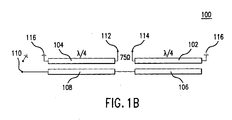
- FIG. 1B illustrates a classic Marchand balun.
- FIG. 2A illustrates a cross section of a coplanar waveguide.
- FIG. 2B illustrates a cross section of a coplanar waveguide with ground.
- FIG. 3 illustrates a coplanar waveguide implantation of the classic Marchand balun.
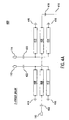
- FIG. 4A illustrates a circuit diagram for a 3-Finger balun according to the present invention.
- FIG. 4B illustrates a circuit diagram for a 4-Finger balun according to the present invention.
- FIG. 5A illustrates a balun according to the present invention.
- FIG. 5B illustrates an embodiment of a balun after calculating element values.
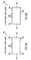
- FIG. 6A illustrates cross section of a two layer printed circuit board without ground plane under the balun traces.
- FIG. 6B illustrates cross section of a two layer printed circuit board with ground plane under the balun traces.
- FIG. 6C illustrates a cross section of four layer printed circuit board without ground plane under the balun traces.
- FIG. 6D illustrates a cross section of four layer printed circuit board with ground plane under the balun traces.
- FIG. 6E illustrates a cross section of six layer printed circuit board without ground plane under the balun traces.
- FIG. 6F illustrates a cross section of six layer printed circuit board with ground plane under the balun traces.
- FIG. 7 illustrates an embodiment of the present invention on a printed circuit board.
- FIG. 8 illustrates an optimized inductor that can be used to transmit DC power or low frequency digital control signals to the center conductor of a balun according to an embodiment of the present invention.
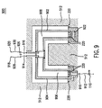
- FIG. 9 illustrates the present invention using three transmission lines and a lumped element matching network.
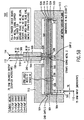
- FIG. 10 illustrates an alternate embodiment of the 3-Finger balun with a ground below the balun according to the present invention.
- FIG. 11 illustrates an inductor for providing DC power or low frequency digital control signals at the balun input in an embodiment of the present invention.
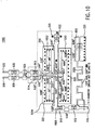
- FIG. 12 illustrates steps of a method for initially designing a balun according to the present invention.
- FIG. 13 illustrates details of the method step of selecting initial design parameters.
- FIG. 14 illustrates details of the method step of simulating balun performance.
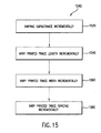
- FIG. 15 illustrates details of the method step of incrementally varying balun parameters.
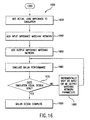
- FIG. 16 illustrates steps of a method for final balun design according to the present invention.
- a data signal122 from a satellite 124 is received at a dish antenna 126 and routed to a low noise block 120.
- low noise block 120 comprises a low noise amplifier, a mixer, an oscillator and an IF amplifier.
- Low noise block 120 amplifies and converts data signal 122 to a desired frequency range from data signal 122 downlink frequency. In one embodiment the desired frequency range is 950-2150 MHz.
- Data signal 122 is passed over a coaxial cable 132 from low noise block 120 to a television set-top box 134.
- Set-top box 134 comprises a tuner circuit138 that converts data signal 122 into a signal suitable for reception by a television 136.
- An example commercial embodiment of tuner 138 is the Broadcom BCM3440A0.
- tuner 138 have a differential radio frequency input in order to achieve the low second-order nonlinear distortion that is critical to a direct conversion receiver architecture.
- a balun 130 is placed between coaxial cable 132 and tuner 138 to convert the unbalanced radio frequency signal carried in coaxial cable 132 to a balanced radio frequency signal 112 and 114 at the input of tuner 138.
- An embodiment of the invention is a balun implemented as a printed metal pattern on a circuit board containing the tuner chip and its ancillary components.
- the printed balun is tolerant of parameter variations during printed circuit board manufacturing. These parameter variations include metal line width, spacing between metal lines, printed circuit board thickness, dielectric constant of the board, and proximity to other metal objects. Tolerance of printed circuit board manufacturing variations enables the printed balun design to be easily incorporated into a standard printed circuit board assembly process.
- the balun output lines should be located close together to interface properly with an integrated circuit package.
- Marchand balun 100 shown in FIG. 1B.
- This classic balun implementation uses two quarter-wavelength sections of coaxial cable inside another coaxial shield.
- One section includes electromagnetically coupled lines 104 and 108, and the other section includes electromagnetically coupled lines 102 and 106.
- the electromagnetic coupling between coaxial line 102 and 106 and between 104 and 108 results in a signal at balun output 112 that is equal in amplitude and opposite in phase to a signal at balun output 114 relative to an input signal at balun input 110.
- a coaxial cable can be flattened and adapted into printable form by cross sectioning the coaxial structure and flattening the conductors into coplanar waveguides.
- a coplanar waveguide 202 comprises a signal trace 206 flanked on both sides by a ground 208. Signal trace 206 and ground 208 are laid on a substrate 212.
- a coplanar waveguide with ground 204 comprises the elements of waveguide 202 and an additional ground 209 under metal trace 206.
- ground 208 can be connected with ground 209 by vias 220 through substrate 212.
- Balun 100 is modified for printed circuit board use by transforming coaxial cable into the coplanar waveguide 202 as illustrated in FIG. 3. Vias 220, also known as plated through holes, provide electrical connection between different layers in multi layer printed circuit boards.
- the coplanar balun 300 consists of balun input 110 coupled to input coplanar waveguide 308.
- First coplanar waveguide 304 and second coplanar waveguide 306 are coupled to balun output 114 and balun output 112, respectively.
- Coplanar waveguides 304 and 306 are coupled to a ground 302. The electromagnetic coupling between coplanar waveguides 304, 306, 308 result in a signal at output 112 that is equal in amplitude and opposite in phase to a signal from balun output 114 relative to an input signal input to balun input 110.
- balun is a conventional two-wire Marchand using a coplanar layout. To achieve the required coupling between the transmission lines is difficult with only two wires. To compensate, a complicated overlay scheme is used which is not compatible with a printed circuit board fabrication process. No size reduction schemes are used, so the balun is undesirably large for use on a printed circuit board.
- a third example of the conventional Marchand balun is discussed in A New Compact Wideband Balun , 1993 IEEE MTT-S Digest, which is incorporated herein by reference in its entirety.
- the balun discussed is made of multiple coupled microstrip lines, so the balun depends critically on dielectric parameters and distance between layers. Multiple lines are used to relax the conductor spacing, but the layout results in the output ports exiting on opposite sides of the balun.
- Balun 400 consists of transmission lines 404,406,408,410,412, and 414.
- Transmission line 404 is coupled to transmission line 406.
- Input capacitor 402 is coupled to transmission line 404 and balun input 110.
- a loading capacitor 418 is coupled to transmission line 406 and a ground 416.
- Transmission lines 408, 410, 412, and 414 are coupled to ground 416.
- Output capacitor 422 is coupled to transmission lines 408, 412 and to positive balun output 112.
- Output capacitor 420 is coupled to transmission lines 410, 414 and to negative balun output 114.
- Transmission lines 404,408, and 412 are electromagnetically coupled.
- Transmission lines 406, 410, and 414 are electromagnetically coupled.
- the electromagnetic coupling between transmission lines 404, 406, 408, 410, 412, and 414 result in a signal at output 112, in response to a signal applied to balun input 110, that is equal in amplitude and opposite in phase to a signal at output 114.
- FIG. 4B is a 4-Finger balun transformer.
- Balun 401 consists of transmission lines 404, 405, 406, 407, 408, 410, 412, and 414.
- Transmission line 404 is coupled to transmission lines 405 and 406.
- Input capacitor 402 is coupled to transmission lines 404, 405 and balun input 110.
- Transmission line 405 is coupled to transmission 407.
- a loading capacitor 418 is coupled to transmission lines 406,407 and to a ground 416.
- Transmission lines 408,410,412, and 414 are coupled to ground 416.
- Output capacitor 422 is coupled to transmission lines 408, 412 and to positive balun output 112.
- Output capacitor 420 is coupled to transmission lines 410,414 and to negative balun output 114.
- Transmission lines 404,405,408, and 412 are electromagnetically coupled.
- Transmission lines 406, 407,410, and 414 are electromagnetically coupled.
- the electromagnetic coupling between transmission lines 404, 405, 406, 407, 408, 410, 412, and 414 result in a signal at output 112, in response to a signal applied to balun input 110, that is equal in amplitude and opposite in phase to a signal at output 114.
- Transmission lines are formed from metal traces. Metal traces provide electrical and electromagnetic coupling. Transmission lines can be configured to function as coplanar waveguide transmission lines or microstrip transmission lines.
- FIG. 5A illustrates printed balun 500, which is a printed metal trace implementation of a balun according to the present invention.
- Printed balun 500 has two metal traces 508, 516 and two connecting traces 501, 514 electrically connected and laid out in a rectangular pattern.
- Metal traces 508 and 516 function as transmission lines.
- Four additional metal traces 520, 524, 534, and 540 are laid parallel to metal traces 508 and 516. Trace 520 and 524 are coupled to a ground 512 and connector 538.
- Metal traces 534 and 540 are coupled to ground 512 and connector 536.
- Metal traces 520, 524, 534, and 540 function as transmission lines.
- Input capacitor 504 is coupled to metal trace 508 and to input inductor 502.
- Input inductor 502 is coupled to balun input 110.
- a loading capacitor 530 is coupled between metal trace 508 and ground 512.
- Balun positive output 112 is coupled to thin metal trace 510.
- Thick metal trace 544 is coupled to thin metal trace 510 and output capacitor 532.
- Output capacitor 532 is coupled to metal trace 534.
- Balun negative output 114 is coupled to thin metal trace 506.
- Thick metal trace 509 is coupled to thin metal trace 506 and output capacitor 526.
- Capacitor 526 is coupled to metal trace 520.
- Electromagnetic coupling between transmission lines 508, 516, 520, 524, 534, and 540 result in a signal at output 112, in response to a signal applied to balun input 110, that is equal in amplitude and opposite in phase to a signal at output 114.
- Inductor 502 and capacitor 504 add an input impedance matching network to balun 500.
- the addition of thick metal traces 544, 509 and thin metal traces 506, 510 add an output impedance matching network to balun 500.
- elements 506, 509, 510, and 544 are distributed elements. Metal trace width, trace spacing, trace proximity to ground and trace thicknesses are varied to achieve the capacitance and inductance values necessary to impedance match with the output circuit.
- elements 506, 509, 510, and 544 can be lumped element components.
- ground 512 is indicated on FIGs. 5, 8, 9, and11 by diagonal lines.
- ground 512 is at the periphery of balun 500.
- Ground 512 can be placed on different layers of the printed circuit board and coupled by vias 220 to the desired layer. In other embodiments ground 512 is placed under the balun.
- balun 500 modifies the classic Marchand balun illustrated in FIGs. 1 and 2 by adding input capacitor 504, loading capacitor 530, output capacitor 532 and output capacitor 526. Coupling these elements to the balun transmission lines provides multiple improvements as discussed below.
- the capacitance of elements 504, 530, 526, 532 is calculated so the balun operates at its most efficient internal impedance.
- Ground 512 is removed from beneath the balun metal traces and placed at the periphery for simplicity of fabrication.
- Four coupled transmission lines are employed rather than two in order to achieve the desired internal balun impedance without requiring the trace spacing to be the manufacturing minimum of 5-mils.
- a high, even mode / odd mode, impedance ratio increases the balun's impedance matching bandwidth and lowers insertion loss across a wider band of input frequencies.
- the added capacitance of elements 504, 530, 526, and 532 electrically lengthens the balun by reducing transmission line wave velocity, thereby enabling the physical length of the transmission lines to be reduced to less than the classic balun's ⁇ /4 length without affecting the unbalanced to balanced signal transformation. Reducing the required transmission line length means the physical size of the balun can be reduced. Reduced size makes it easier for a circuit designer to implement the balun on a crowded printed circuit board.
- a further improvement to the classic Marchand balun is the addition of impedance matching networks at the balun input and outputs.
- the input matching network consists of inductor 502 and capacitor 504 series coupled at balun input 110.
- the output matching network consists of thick metal trace 509 coupled to thin metal trace 506, which is coupled to balun output 114. Thick metal trace 544 is coupled in series with thin metal trace 510, which is coupled to the balun output 112.
- These networks are designed to match the input impedance of the balun to the impedance of the input circuitry and the output impedance of the balun to the impedance of the output circuit.
- the matched input and output impedances provide improved signal transfer between the input and output circuits while the internal balun impedance is unaffected and optimized for high bandwidth, low loss and other factors.
- the output impedance value is selected to match the circuitry coupled to the balun output. This impedance is typically 50 or 75 ohms, but is variable to match other circuit values.
- the input and output matching networks can be constructed from lumped elements or distributed elements.
- a person skilled in the art will understand the advantages and disadvantages of both types of elements.
- baluns illustrated in FIG. 5A are placed on the top layer of a printed circuit board. This simplifies balun construction and makes it more tolerant to manufacturing changes in printed circuit board layer width, dielectric constant, and printed trace dimensions.
- a lower metal layer can function to connect metal traces.
- surface mount zero-ohm chip resistors can be used.
- Balun 501 has the following electrical characteristics:
- coplanar waveguide makes a ground under the balun traces optional, since the necessary configuration can be set on a single layer. Some embodiments use a ground under the balun metal traces to achieve better isolation and shielding from external noise sources.
- FIGs. 6A-6F different arrangements of balun metal traces 206, ground 208 and ground 209 are illustrated. Vias 220 is used to connect ground 208, 209 together across printed circuit board (PCB) layers.
- FIG. 6A illustrates a two-layer PCB 602 with balun traces 206, ground 208 and vias 220 connecting ground 208 to ground 209.
- FIG. 6B illustrates a two-layer PCB 604 with ground 209 under balun traces 206.
- FIG. 6C illustrates a four-layer PCB 606 without ground 209 under balun traces 206.
- FIG. 6D illustrates a four-layer PCB 608 with ground 209 under balun traces 206.
- FIG. 6E illustrates a six-layer PCB 610 without ground 209 under balun traces 206.
- FIG. 6F illustrates a six-layer PCB 612 with ground 209 under balun traces 206.
- Balun 500 can be embodied in any of the printed board cross sections described in FIGs. 6A-6F as well as additional cross section arrangements that one of skill in the art would recognize based on the teachings herein.
- balun 500 uses four coupled coplanar waveguides to strengthen the electromagnetic coupling, making the balun tolerant to variation in printed circuit board materials, dimensions and customer layout. Inexpensive lumped components can be used for tuning and impedance matching to a capacitive balun input.
- the geometry of the output lines functions as a distributed tuning network to provide another degree of freedom in matching the balun to a particular integrated circuit.
- Other embodiments use three couples transmission lines to achieve the desired performance.
- FIG. 7 illustrates printed circuit 700, which is a printed circuit embodiment of the invention.
- Printed circuit 700 is balun 500 coupled to a radio frequency signal input 702 at balun input 110.
- Capacitor 706 is a one picofarad capacitor coupled approximately 425 mils from balun input 110.
- Balun output 112 and balun output 114 are coupled to a tuner 704.
- tuner 704 is the Broadcom BCM3440A0.
- FIG. 8 illustrates an apparatus for transferring direct current power and low frequency digital control signals to low noise block 120 adapted for use with balun 500.
- Direct current power is defined as power supplied from a current source as direct current or from a voltage source as direct voltage.
- low frequency digital control signals can be supplied to low noise block 120.
- a direct current power and low frequency digital control signal source 802 is coupled to spiral inductor 810. Direct current power and low frequency digital control signals can be supplied from source 802 together or either signal separately.
- Spiral inductor 810 is connected to balun radio frequency input 702, approximately 425 mils from balun input 110.
- Radio frequency input 702 is connected to coaxial cable 132.
- Coaxial cable 132 is connected to low noise block 120.
- a capacitor 804 is also coupled to ground 512 and to radio frequency input 702 approximately 425 mils from balun input 110. Capacitor 804 and inherent capacitance from the connection of spiral inductor 810 reduce undesirable cross over interference at balun input 110.
- Ground 512 is provided from vias 220. Individual vias are shown as solid dots but, for clarity, each is not labeled..
- Spiral inductor 810 is designed to provide a very high impedance at the signal frequency of interest at balun input 110. Connection of spiral inductor 810 to balun input 110 has negligible loading effect on balun 500 and radio frequency input 702. The high impedance of spiral inductor 810 does not affect the transmission of direct current power or low frequency digital control signals.
- Spiral inductor 810 coupled to balun 500 is an embodiment of the present invention to provide direct current power and low frequency digital control signals along coaxial cable 132 to power low noise block 120. This embodiment does not deleteriously affect the radio frequency signal at balun input 110 or the electrical characteristics of the balun.
- FIG. 9 illustrates balun 900, which is an embodiment of the present invention that uses lumped capacitive and inductive components and three coupled transmission lines.
- Balun 900 consists of a first input transmission line 902 electrically coupled to a second input transmission line 904 and laid out in a rectangular pattern.
- a first output transmission line 906 is coupled to a second output transmission line 908 and to ground 512.
- Input transmission lines 902 and 904 are coupled to an input capacitor 910.
- An input inductor 912 is coupled to input capacitor 910 and to balun input 110.
- First output transmission line 906 is coupled to an output capacitor 914.
- Output capacitor 914 is coupled to an output inductor 928.
- Output inductor 928 is coupled to a positive balun output 918.
- Second output transmission line 908 is coupled to an output capacitor 916.
- Output capacitor 916 is coupled to an output inductor 930.
- Output inductor 930 is coupled to a negative balun output 920. Electromagnetic coupling between transmission lines 904 and 906 and electromagnetic coupling between 902 and 908 result in a signal at balun output 918 in response to a signal applied to balun input 110, which is equal in amplitude and opposite in phase to a signal at output 920.
- a loading capacitor 922 is coupled to transmission lines 902 and 904 and to ground 512.
- Loading capacitor 922 is equivalent to capacitor 530.
- Capacitor 922 can be fabricated as a distributed or a lumped element capacitor.
- a tuning capacitor 926 is coupled across the outputs of capacitor 914 and capacitor 916. Capacitor 926 provides a differential capacitance on balun 900 to allow finer tuning of the internal balun impedance and thereby reduce input return loss.
- Ground 512 is provided from vias 220. Individual vias are shown as solid dots but, for clarity, each is not labeled.
- FIG. 10 illustrates balun 1000 which is an embodiment of the present invention.
- Balun 1000 has balun input 110 coupled to input capacitor 912.
- Capacitor 912 is connected to inductor 910.
- An input transmission line 1006 is coupled to inductor 910 and to loading capacitor 922.
- Capacitor 922 is coupled between transmission line 1006 and ground 512.
- Transmission lines 1002, 1004, and 1010 are electrically coupled to output capacitor 914 and output capacitor 916.
- Output inductor 930 is connected to balun negative output 920.
- Output inductor 928 is connected to output capacitor 914 and balun positive output 918.
- Tuning capacitor 926 is connected between the output side of capacitors 914 and 916.
- Transmission line 1006 is electromagnetically coupled to transmission lines 1002, 1004, and 1010 that results in a signal at output 918, in response to a signal applied to balun input 110, that is equal in amplitude and opposite in phase to a signal at output 920.
- Ground 512 is provided from vias 220. Individual vias are shown as solid dots but, for clarity, each is not labeled. Also for clarity, diagonal lines are not used to show the location of ground 512. Elements containing vias 220 are coupled to ground 512. In the embodiment shown in FIG. 10 ground 512 is located on layer two under everything except balun. There is also a ground on layer four located beneath everything.
- FIG. 10 also illustrates an embodiment of a device used to provide direct current and voltage power or low frequency digital control signals to low noise block 120.
- Direct current power and low frequency digital control signal source 802 is coupled to meandered trace 1025.
- Trace 1025 is coupled to balun 1000 between input 110 and input capacitor 912.
- Meandered trace 1025 provides a high impedance to data signal122 to minimize undesired electrical loading of balun 1000 and low noise block 120.
- FIG. 11 illustrates an alternate embodiment of a spiral inductor used to transfer direct current power and low frequency digital control signals to coaxial cable 132.
- Spiral inductor 1100 has direct current power and low frequency digital control signal source 802.
- a connection 1120 couples spiral 1100 to balun input 110.
- Ground 512 is provided from vias 220. Individual vias are shown as solid dots but, for clarity, each is not labeled. Ground 512 is also located under the spiral elements. For clarity the ground under spiral inductor 1100 is not illustrated with diagonal lines. The top layer ground 512 is shown with diagonal lines.
- inductor 1100 The high impedance exhibited by inductor 1100 does not effect the operation of balun 500 or coaxial cable 132 at signal 122 frequencies of 950 to 2150 MHZ. Direct current power and low frequency digital control signals are unaffected by the high impedance. The direct current power and low frequency digital control signals are placed on the center connector of coaxial cable 132 and applied to low noise block 120.
- Inductor 1100 is an embodiment of inductor 800 modified to function with ground under the metal traces. Spiral inductor 1100 can be used in place of meandered trace 1025 for coupling direct current power and low frequency digital control signal source 802 to balun input 110.
- FIG. 12 illustrates a method for initial design of a balun according to the present invention.
- a design for the balun is selected.
- the performance of the balun is simulated.
- the performance of the balun is compared with the design goal performance. If the simulated performance is equal or better than design goal performance, the initial design is complete, step 1250. If simulated performance is less than design goal performance the existing parameters are varied, step 1240. Then step 1220 is performed again to simulate the balun performance. Steps 1220, 1230 and 1240 continue until the initial balun design is complete in step 1250.
- Step 1210 is shown in further detail in FIG. 13.
- an initial length, width and spacing of the metal traces are selected. These values are the balun designer's best estimates of the components and configuration necessary to achieve the balun design goals.
- initial physical size constraints and an initial metal trace layout are selected. These constraints account for any size or configuration constraints placed on the balun design in its intended use.
- an initial ground plane configuration is selected.
- an initial value is selected for individual capacitors 404, 410, 426, and 432.
- Step 1220 is shown in further detail in FIG. 14.
- the balun parameters are encoded in a simulator.
- the balun simulation is driven with a characteristic input impedance. In an embodiment the input impedance is 75 ohms.
- the balun is loaded with a substantially balanced differential load. This output load is a simplification of the load expected in the actual circuit embodiment. An ideal value is selected to allow the balun simulation to more easily converge on a solution.
- the substantially balanced differential load does not reflect the floating load anticipated in an actual circuit embodiment of the balun.
- the balun passband insertion loss, input return loss, bandwidth and differential signal balance are calculated by the simulator.
- Step 1240 is shown in further detail in FIG. 15.
- step 1520 the value of a capacitor is varied incrementally in a manner to result in balun performance closer to the design goal.
- an example of the specific capacitors varied in this step are the input capacitor 404, the loading capacitor 410, output capacitor 426, and output capacitor 432.
- step 1540 the printed metal trace lengths are varied incrementally in a manner to result in balun performance closer to the design goal.
- the printed trace widths are varied incrementally in a manner to result in balun performance closer to the design goal.
- step 1580 the printed metal trace spacing is varied incrementally in a manner to result in balun performance closer to the design goal.
- FIG. 16 illustrates the method of final balun design.
- Step 1250 occurs after the balun initial design is complete.
- step 1620 the actual load impedance is encoded in the balun simulator.
- step 1640 an impedance matching network is coupled to the balun input.
- step 1650 an impedance matching network is coupled to each side of the balun differential output.
- step 1660 the balun performance is simulated.
- step 1670 the balun simulated performance is compared with design goal performance. If simulated is equal or greater than design goal performance, step 1690 is performed.
- step 1690 balun design is completed. If simulated performance is less than a design goal, step 1680 is performed.
- step 1680 the value of an element in the input and output matching networks is varied incrementally in a manner to result in balun performance closer to the design goal. Then step 1660 is performed. Steps 1660, 1670, and 1680 are performed in sequence until simulated balun performance is equal to or better than design goal performance.
Landscapes
- Engineering & Computer Science (AREA)
- Microelectronics & Electronic Packaging (AREA)
- Coils Or Transformers For Communication (AREA)
Abstract
Description
Claims (34)
- A balun, comprising:a first capacitor coupled to an input;a plurality of first coupled metal traces coupled to said first capacitor;a plurality of second coupled metal traces, said second coupled metal traces electromagnetically coupled to said first coupled metal traces;a ground coupled to said second coupled metal traces;a first output coupled to said second coupled metal traces;a second output coupled to said second coupled metal traces;a second capacitor coupled between said first coupled metal traces and said ground;a third capacitor coupled to said first output; anda fourth capacitor coupled to said second output.
- The balun of claim 1, wherein said first coupled metal traces and said second coupled metal traces are located on a surface layer of a printed circuit board.
- The balun of claim 1, wherein said first coupled metal traces and said second coupled metal traces are located on the same layer of a printed circuit board.
- The balun of any of claims 1 to 3, wherein said ground is placed beneath said first coupled metal traces and said second coupled metal traces.
- The balun of any of claims 1 to 3, wherein said ground is placed at a periphery of said first coupled metal traces and said second coupled metal traces.
- The balun of any of the preceding claims, further comprising:a fifth capacitor coupled between said first output and said second output.
- The balun of any of the preceding claims, wherein said first output provides a signal having an equal amplitude and opposite phase to a signal provided from said second output in response to a signal input to said input.
- The balun of any of the preceding claims, wherein said first coupled metal traces and said second coupled metal traces are transmission lines.
- The balun of claim 8, wherein said plurality of first coupled transmission lines comprises one first coupled transmission line or two first coupled transmission lines.
- The balun of claim 8 or claim 9, wherein a longitudinal dimension of said transmission lines is less than one-quarter wavelength of said input signal.
- The balun of any of claims 8 to 10, wherein said transmission lines are coplanar waveguide transmission lines or microstrip transmission lines.
- The balun of any of the preceding claims, further comprising a first impedance matching network coupled to said input and a second impedance matching network coupled to said first output and said second output.
- The balun of claim 12, wherein said first impedance matching network comprises a fifth capacitor series coupled to an inductor.
- The balun of claim 12 or claim 13, wherein said second impedance matching network comprises:two coupled metal traces, wherein at least one of a metal trace width, a metal trace spacing and a metal trace thickness is adjusted to provide a desired output impedance.
- The balun of claim 14, wherein said second impedance matching network comprises lumped element components.
- The balun of any of the preceding claims, wherein an input impedance of said balun is approximately 50 to 75 ohms.
- The balun of any of the preceding claims, wherein the output impedance of said balun is a desired value.
- The balun of any of the preceding claims, wherein a direct current power and low frequency digital control signal source is coupled to said input.
- The balun of claim 18, wherein a metal trace is coupled between said direct current power and low frequency digital control signal source and said input, wherein said metal trace does not effect said balun's electrical characteristics over a desired frequency range.
- The balun of claim 19, wherein said metal trace is a spiral inductor.
- The balun of claim 20, wherein said inductor is coupled to said input approximately 425 mils from said input.
- A balun comprising:a plurality of coupled metal traces;an input, coupled to said metal traces;an output, coupled to said metal traces,means for producing output signals having an equal amplitude and opposite phase responsive to an input signal received at said input, and means for reducing a physical dimension of said metal traces.
- The balun of claim 22, further comprising:means for applying direct current power and low frequency digital control signals to said metal traces without electrically loading said balun over a desired frequency band.
- The balun of claim 23, wherein said desired frequency range is approximately 950 to 2150 megahertz.
- An integrated circuit, comprising:wherein said electrically unbalanced input is impedance matched to said first circuit and said electrically balanced electrical output is impedance matched to said second circuit.a capacitively loaded balun;a first circuit, coupled to an electrically unbalanced input of said capacitively loaded balun;a second circuit, coupled to an electrically balanced output of said capacitively loaded balun;
- The integrated circuit of claim 25, further comprising:a metal trace coupled to said electrically unbalanced input, said metal trace having a high impedance to an input signal over a desired frequency range.
- The integrated circuit of claim 26, wherein said metal trace is a spiral inductor.
- The integrated circuit of claim 26 or claim 27, wherein said desired frequency range is approximately 950 to 2150 megahertz.
- A method of designing an improved printed trace balun, comprising the steps of:(1) selecting balun design parameters;(2) simulating said balun performance;(3) comparing said simulated performance with a design goal performance;(4) incrementally varying said balun design parameters; and(5) repeating steps 2 through 4 until said simulated balun performance is equal or better than design goal performance.
- The method of claim 29, wherein step 1 comprises the following steps:(a) selecting an initial metal trace length, an initial metal trace spacing, and an initial metal trace spacing;(b) selecting an initial balun size and trace layout, wherein said initial balun size and trace layout are a function of step (a);(c) selecting an initial ground plane configuration; and(d) selecting an initial capacitor value.
- The method of claim 29 or claim 30, wherein step 2 comprises the following steps:(a) encoding said balun parameters in a simulator;(b) driving said balun with an input circuit having a characteristic input impedance;(c) loading said balun with a substantially balanced differential load; and(d) calculating passband insertion loss, input return loss, bandwidth, and differential signal balance based on steps(a) through (c).
- The method of any of claims 29 to 31, wherein step 4 comprises the following steps:(a) varying a value of a capacitor incrementally;(b) varying a length of a printed metal trace incrementally;(c) varying a width of said printed trace incrementally; and(d) varying a spacing of said printed trace incrementally, wherein said varying is selected to result in balun performance closer to a design goal.
- The method of claim 32, wherein step 4 further comprises:(e) adjusting the symmetry of said balun by incrementally varying the lengths of said metal traces on one side of the balun.
- The method of any of claims 29 to 33, wherein step 5 further comprises:(a) adding an actual load impedance to a simulator;(b) adding an input impedance matching network to said balun;(c) adding an output impedance matching network to said balun;(d) simulating a balun performance;(e) comparing said performance to said design goal;(f) incrementally varying at least one component of said input and said output impedance matching networks, wherein said varying step is performed to move said balun performance closer to a design goal; and(g) performing said simulating and said comparing steps until said simulated balun performance is equal to or better than said design goal performance.
Applications Claiming Priority (4)
| Application Number | Priority Date | Filing Date | Title |
|---|---|---|---|
| US26262901P | 2001-01-22 | 2001-01-22 | |
| US262629P | 2001-01-22 | ||
| US892755 | 2001-06-28 | ||
| US09/892,755 US6819199B2 (en) | 2001-01-22 | 2001-06-28 | Balun transformer with means for reducing a physical dimension thereof |
Publications (2)
| Publication Number | Publication Date |
|---|---|
| EP1227537A2 true EP1227537A2 (en) | 2002-07-31 |
| EP1227537A3 EP1227537A3 (en) | 2003-06-11 |
Family
ID=26949357
Family Applications (1)
| Application Number | Title | Priority Date | Filing Date |
|---|---|---|---|
| EP02250408A Ceased EP1227537A3 (en) | 2001-01-22 | 2002-01-21 | Balun transformer for a satellite television tuner |
Country Status (2)
| Country | Link |
|---|---|
| US (2) | US6819199B2 (en) |
| EP (1) | EP1227537A3 (en) |
Cited By (1)
| Publication number | Priority date | Publication date | Assignee | Title |
|---|---|---|---|---|
| EP1416575A1 (en) | 2002-10-30 | 2004-05-06 | STMicroelectronics S.A. | Balun transformer |
Families Citing this family (55)
| Publication number | Priority date | Publication date | Assignee | Title |
|---|---|---|---|---|
| US20020121707A1 (en) * | 2001-02-27 | 2002-09-05 | Chippac, Inc. | Super-thin high speed flip chip package |
| US8143108B2 (en) | 2004-10-07 | 2012-03-27 | Stats Chippac, Ltd. | Semiconductor device and method of dissipating heat from thin package-on-package mounted to substrate |
| US7138884B2 (en) * | 2002-08-19 | 2006-11-21 | Dsp Group Inc. | Circuit package integrating passive radio frequency structure |
| US20040201539A1 (en) * | 2003-04-09 | 2004-10-14 | Yewen Robert G. | Radio frequency identification system and antenna system |
| ATE442681T1 (en) * | 2004-09-30 | 2009-09-15 | Taiyo Yuden Kk | PUSH-PULT FILTER DEVICE |
| US7250828B2 (en) * | 2005-03-16 | 2007-07-31 | Tdk Corporation | Compact balun |
| KR100570103B1 (en) * | 2005-03-30 | 2006-04-11 | 삼성전자주식회사 | Memory Modules and Memory Systems with Matched Capacitors |
| US7265644B2 (en) * | 2005-04-01 | 2007-09-04 | International Business Machines Corporation | Ultra-broadband integrated balun |
| US7646261B2 (en) * | 2005-09-09 | 2010-01-12 | Anaren, Inc. | Vertical inter-digital coupler |
| JP2007189396A (en) * | 2006-01-12 | 2007-07-26 | Seiko Epson Corp | Balun |
| US7605672B2 (en) * | 2006-02-02 | 2009-10-20 | Anaren, Inc. | Inverted style balun with DC isolated differential ports |
| EP1987562A4 (en) * | 2006-02-02 | 2009-04-22 | Anaren Inc | Inverted style balun with dc isolated differential ports |
| US20070223615A1 (en) * | 2006-03-24 | 2007-09-27 | Sathwant Dosanjh | Transceiver interface architecture |
| US7528676B2 (en) * | 2007-04-16 | 2009-05-05 | Tdk Corporation | Balun circuit suitable for integration with chip antenna |
| DE102007021899B4 (en) | 2007-04-17 | 2018-05-17 | Rohde & Schwarz Gmbh & Co. Kg | Microwave circuit with Defected Ground Structure Filter |
| US8106739B2 (en) * | 2007-06-12 | 2012-01-31 | Advanced Magnetic Solutions United | Magnetic induction devices and methods for producing them |
| DE102008024898B4 (en) * | 2008-05-28 | 2015-01-22 | Epcos Ag | Broadband RF power divider circuit |
| US8508313B1 (en) * | 2009-02-12 | 2013-08-13 | Comtech Xicom Technology Inc. | Multiconductor transmission line power combiner/divider |
| US7880557B2 (en) * | 2009-03-12 | 2011-02-01 | Hittite Microwave Corporation | Hybrid marchand/back-wave balun and double balanced mixer using same |
| US8354892B2 (en) * | 2009-11-03 | 2013-01-15 | Electronics And Telecommunications Research Institute | Marchand balun device for forming parallel and vertical capacitance |
| EP2586125A4 (en) | 2010-06-22 | 2014-06-18 | Hittite Microwave Corp | Improved double balanced mixer |
| US8653904B2 (en) * | 2010-06-25 | 2014-02-18 | Tdk Corporation | Thin film balun |
| US8362849B2 (en) | 2010-07-20 | 2013-01-29 | Raytheon Company | Broadband balun |
| JP5516738B2 (en) * | 2010-07-27 | 2014-06-11 | 株式会社村田製作所 | High frequency module |
| KR101394965B1 (en) | 2010-10-14 | 2014-05-16 | 한국전자통신연구원 | Wavelength tunable external cavity laser generating device |
| CN102623777B (en) * | 2011-01-27 | 2014-06-18 | 鸿富锦精密工业(深圳)有限公司 | Low-pass filter |
| TWI513100B (en) * | 2011-07-01 | 2015-12-11 | Avermedia Tech Inc | Rf signal transmitting circuit applied to electronic apparatus |
| TW201316680A (en) * | 2011-10-12 | 2013-04-16 | Hon Hai Prec Ind Co Ltd | Marchand balun circuit with matching circuit |
| FR2981753A1 (en) * | 2011-10-24 | 2013-04-26 | St Microelectronics Crolles 2 | VARIABLE IMPEDANCE DEVICE |
| US9059494B2 (en) | 2013-01-18 | 2015-06-16 | International Business Machines Corporation | Marchand balun structure and design method |
| US9329255B2 (en) * | 2013-06-24 | 2016-05-03 | Raytheon Company | Imaging antenna and related techniques |
| EP2899803B1 (en) | 2014-01-24 | 2020-06-24 | Ampleon Netherlands B.V. | Circuit comprising balun and impedance transforming elements |
| CN106716778A (en) * | 2014-06-26 | 2017-05-24 | 索雷斯能源公司 | Wireless electric field power transmission system, transmitter and receiver therefor and method of wirelessly transferring power |
| CN105356858B (en) * | 2014-08-19 | 2018-05-11 | 华为技术有限公司 | A kind of balun and power amplifier |
| CN107005092B (en) | 2014-09-05 | 2020-03-10 | 索雷斯能源公司 | Radio field power transfer system, method and transmitter and receiver thereof |
| TWI552521B (en) * | 2014-09-19 | 2016-10-01 | Univ Nat Taiwan | Electromagnetic Noise Filter and Its Equivalent Filter Circuit |
| US9763333B2 (en) * | 2015-03-09 | 2017-09-12 | Cooper Technologies Company | Shared resistor pad bypass |
| US10312565B1 (en) | 2015-03-30 | 2019-06-04 | David B. Aster | Microwave power divider/combiner devices, microwave power divider/combiner bandpass filters, and methods of thermally cooling a cable run |
| US9947986B1 (en) | 2015-03-30 | 2018-04-17 | David B. Aster | Reactive power combiners and dividers including nested coaxial conductors |
| US9812756B1 (en) | 2015-03-30 | 2017-11-07 | David B. Aster | Systems and methods for combining or dividing microwave power using satellite conductors and capable of receiving and retaining a gas |
| US9793593B1 (en) | 2015-03-30 | 2017-10-17 | David B. Aster | Power combiners and dividers including cylindrical conductors and capable of receiving and retaining a gas |
| US9673503B1 (en) | 2015-03-30 | 2017-06-06 | David B. Aster | Systems and methods for combining or dividing microwave power |
| US9960469B1 (en) | 2015-03-30 | 2018-05-01 | David B. Aster | Broadband reactive power combiners and dividers including nested coaxial conductors |
| JP6511962B2 (en) * | 2015-05-28 | 2019-05-15 | Tdk株式会社 | Stacked electronic components |
| US9843301B1 (en) | 2016-07-14 | 2017-12-12 | Northrop Grumman Systems Corporation | Silicon transformer balun |
| JP6885016B2 (en) * | 2016-10-28 | 2021-06-09 | Tdk株式会社 | Balun |
| CN107039728A (en) * | 2017-03-18 | 2017-08-11 | 深圳市景程信息科技有限公司 | Five assistant wardens connection coupled line structure in wideband balun |
| JP7051649B2 (en) * | 2018-09-07 | 2022-04-11 | 株式会社東芝 | Magnetic coupling device and communication system |
| US10911016B2 (en) | 2019-01-08 | 2021-02-02 | Analog Devices, Inc. | Wideband balun |
| US11101227B2 (en) | 2019-07-17 | 2021-08-24 | Analog Devices International Unlimited Company | Coupled line structures for wideband applications |
| CN112073023B (en) * | 2020-09-02 | 2024-11-08 | 成都芯川电子有限公司 | Wideband High Balance Balun |
| US12015388B2 (en) * | 2021-05-28 | 2024-06-18 | Bae Systems Information And Electronic Systems Integration Inc. | Broadband microwave and millimeter-wave balanced-to-unbalanced transformer |
| CN113594654B (en) * | 2021-07-30 | 2023-10-27 | 上海联影医疗科技股份有限公司 | Planar balun |
| US12424721B2 (en) * | 2023-02-01 | 2025-09-23 | Macom Technology Solutions Holdings, Inc. | Wideband passive balun including separate first and second high-pass filters having inputs thereof resistively connected to ground |
| WO2026034000A1 (en) * | 2024-08-06 | 2026-02-12 | ソニーセミコンダクタソリューションズ株式会社 | Semiconductor package, imaging device, electronic device, and method for manufacturing semiconductor package |
Family Cites Families (7)
| Publication number | Priority date | Publication date | Assignee | Title |
|---|---|---|---|---|
| US5644272A (en) * | 1996-03-05 | 1997-07-01 | Telefonaktiebolaget Lm Ericsson | High frequency balun provided in a multilayer substrate |
| US5697088A (en) * | 1996-08-05 | 1997-12-09 | Motorola, Inc. | Balun transformer |
| FI103614B (en) * | 1997-03-20 | 1999-07-30 | Nokia Mobile Phones Ltd | Phasing and balancing means |
| JP3528044B2 (en) * | 1999-04-06 | 2004-05-17 | 株式会社村田製作所 | Dielectric filter, dielectric duplexer and communication device |
| DE19943955A1 (en) * | 1999-09-14 | 2001-04-12 | Bosch Gmbh Robert | Balun |
| US6538077B1 (en) * | 1999-11-04 | 2003-03-25 | Phillips Petroleum Company | Polymerization catalyst systems, methods of making and uses therefor |
| US6483415B1 (en) * | 2001-05-21 | 2002-11-19 | Industrial Technology Research Institute | Multi-layer LC resonance balun |
-
2001
- 2001-06-28 US US09/892,755 patent/US6819199B2/en not_active Expired - Lifetime
-
2002
- 2002-01-21 EP EP02250408A patent/EP1227537A3/en not_active Ceased
-
2004
- 2004-11-10 US US10/984,771 patent/US7215218B2/en not_active Expired - Fee Related
Cited By (3)
| Publication number | Priority date | Publication date | Assignee | Title |
|---|---|---|---|---|
| EP1416575A1 (en) | 2002-10-30 | 2004-05-06 | STMicroelectronics S.A. | Balun transformer |
| US7864014B2 (en) | 2002-10-30 | 2011-01-04 | Stmicroelectronics, Sa | Mode-switching transformer |
| US8063729B2 (en) | 2002-10-30 | 2011-11-22 | Stmicroelectronics, S.A. | Mode-switching transformer |
Also Published As
| Publication number | Publication date |
|---|---|
| US7215218B2 (en) | 2007-05-08 |
| US20020097107A1 (en) | 2002-07-25 |
| US20050088252A1 (en) | 2005-04-28 |
| US6819199B2 (en) | 2004-11-16 |
| EP1227537A3 (en) | 2003-06-11 |
Similar Documents
| Publication | Publication Date | Title |
|---|---|---|
| US6819199B2 (en) | Balun transformer with means for reducing a physical dimension thereof | |
| EP0885469B1 (en) | A high frequency balun provided in a multilayer substrate | |
| US6825738B2 (en) | Reduced size microwave directional coupler | |
| US7755447B2 (en) | Multilayer balun, hybrid integrated circuit module, and multilayer substrate | |
| US7026884B2 (en) | High frequency component | |
| US7528676B2 (en) | Balun circuit suitable for integration with chip antenna | |
| EP1366539B1 (en) | Coupling device using buried capacitors in multilayered substrate | |
| JPH10173410A (en) | Transmission circuit using stripline | |
| US6636126B1 (en) | Four port hybrid | |
| Zhou et al. | Overview of common-mode noise suppression techniques: From reflection to absorption | |
| CN108123196B (en) | Broadband filtering integrated stereo balun based on vertical double-sided parallel strip lines | |
| US20170026201A1 (en) | Wideband rf device | |
| JPH08162812A (en) | High frequency coupler | |
| CN1964595A (en) | A matching capacitor and PCB using same and impedance matching device | |
| JP3175876B2 (en) | Impedance transformer | |
| EP1845581B1 (en) | Multilayer planar balun transformer, mixers and amplifiers | |
| US20250062519A1 (en) | Ultra wideband board-to-board transitions for stripline rf transmission lines | |
| Piekarz et al. | High‐performance differentially fed coupled‐line directional couplers realised in inhomogeneous medium | |
| CN101752350A (en) | Multi-layer complementary metal transmission line structure | |
| CN119786929B (en) | Dual-Ground Metal-Free Through-Hole All-Metal Integrated Waveguide Structure | |
| CN117578056A (en) | Coaxial Microstrip Conversion Circuit | |
| KR100543214B1 (en) | Microstrip-to-coaxial vertical transition | |
| CN117223400A (en) | Differential Pair Impedance Matching for Printed Circuit Boards | |
| CN121124756A (en) | An ultra-wideband bias circuit and its integrated structure. | |
| WO2007092725A2 (en) | Inverted style balun with dc isolated differential ports |
Legal Events
| Date | Code | Title | Description |
|---|---|---|---|
| PUAI | Public reference made under article 153(3) epc to a published international application that has entered the european phase |
Free format text: ORIGINAL CODE: 0009012 |
|
| AK | Designated contracting states |
Kind code of ref document: A2 Designated state(s): AT BE CH CY DE DK ES FI FR GB GR IE IT LI LU MC NL PT SE TR |
|
| AX | Request for extension of the european patent |
Free format text: AL;LT;LV;MK;RO;SI |
|
| PUAL | Search report despatched |
Free format text: ORIGINAL CODE: 0009013 |
|
| AK | Designated contracting states |
Designated state(s): AT BE CH CY DE DK ES FI FR GB GR IE IT LI LU MC NL PT SE TR |
|
| AX | Request for extension of the european patent |
Extension state: AL LT LV MK RO SI |
|
| 17P | Request for examination filed |
Effective date: 20031211 |
|
| AKX | Designation fees paid |
Designated state(s): AT BE CH CY DE DK ES FI FR GB GR IE IT LI LU MC NL PT SE TR |
|
| RAP1 | Party data changed (applicant data changed or rights of an application transferred) |
Owner name: BROADCOM CORPORATION |
|
| 17Q | First examination report despatched |
Effective date: 20071220 |
|
| STAA | Information on the status of an ep patent application or granted ep patent |
Free format text: STATUS: THE APPLICATION HAS BEEN REFUSED |
|
| 18R | Application refused |
Effective date: 20091125 |