EP1227499A1 - Non-volatile electrically alterable semiconductor memory - Google Patents
Non-volatile electrically alterable semiconductor memory Download PDFInfo
- Publication number
- EP1227499A1 EP1227499A1 EP01830039A EP01830039A EP1227499A1 EP 1227499 A1 EP1227499 A1 EP 1227499A1 EP 01830039 A EP01830039 A EP 01830039A EP 01830039 A EP01830039 A EP 01830039A EP 1227499 A1 EP1227499 A1 EP 1227499A1
- Authority
- EP
- European Patent Office
- Prior art keywords
- column
- columns
- memory cells
- memory
- packet
- Prior art date
- Legal status (The legal status is an assumption and is not a legal conclusion. Google has not performed a legal analysis and makes no representation as to the accuracy of the status listed.)
- Granted
Links
- 239000004065 semiconductor Substances 0.000 title claims abstract description 47
- 230000015654 memory Effects 0.000 claims abstract description 239
- 238000000034 method Methods 0.000 claims description 3
- 230000009466 transformation Effects 0.000 claims description 3
- 101000741396 Chlamydia muridarum (strain MoPn / Nigg) Probable oxidoreductase TC_0900 Proteins 0.000 abstract description 4
- 101000741399 Chlamydia pneumoniae Probable oxidoreductase CPn_0761/CP_1111/CPj0761/CpB0789 Proteins 0.000 abstract description 4
- 101000741400 Chlamydia trachomatis (strain D/UW-3/Cx) Probable oxidoreductase CT_610 Proteins 0.000 abstract description 4
- 239000000758 substrate Substances 0.000 description 21
- 239000000969 carrier Substances 0.000 description 4
- 230000000694 effects Effects 0.000 description 3
- 239000002800 charge carrier Substances 0.000 description 2
- 238000002347 injection Methods 0.000 description 2
- 239000007924 injection Substances 0.000 description 2
- 239000011159 matrix material Substances 0.000 description 2
- 230000007246 mechanism Effects 0.000 description 2
- 239000000243 solution Substances 0.000 description 2
- 230000009471 action Effects 0.000 description 1
- 239000000872 buffer Substances 0.000 description 1
- 230000008859 change Effects 0.000 description 1
- 230000005684 electric field Effects 0.000 description 1
- 238000005516 engineering process Methods 0.000 description 1
- 230000002349 favourable effect Effects 0.000 description 1
- 239000002784 hot electron Substances 0.000 description 1
- 238000004519 manufacturing process Methods 0.000 description 1
- 238000005036 potential barrier Methods 0.000 description 1
- 230000000644 propagated effect Effects 0.000 description 1
- 230000009467 reduction Effects 0.000 description 1
Images


Classifications
-
- G—PHYSICS
- G11—INFORMATION STORAGE
- G11C—STATIC STORES
- G11C16/00—Erasable programmable read-only memories
- G11C16/02—Erasable programmable read-only memories electrically programmable
- G11C16/06—Auxiliary circuits, e.g. for writing into memory
- G11C16/08—Address circuits; Decoders; Word-line control circuits
-
- G—PHYSICS
- G11—INFORMATION STORAGE
- G11C—STATIC STORES
- G11C7/00—Arrangements for writing information into, or reading information out from, a digital store
- G11C7/18—Bit line organisation; Bit line lay-out
Definitions
- the present invention relates generally to the field of semiconductor memory devices, and more particularly to non-volatile memories. Still more particularly, the invention relates to electrically erasable and programmable non-volatile memories such as Flash memories.
- Flash memories offer the possibility of writing data per single Bytes or words (of two or multiple of two Bytes). On the contrary, when even a single data Byte or word stored in the memory is to be modified, it is necessary to erase the information stored in the whole memory or, at the best, in a whole memory sector containing such Byte or word.
- a two-dimensional array of memory cells which can be the whole memory matrix or a memory sector of a Flash memory.
- the memory cells are conventionally arranged in rows (word lines) and columns (bit lines).
- a plurality of P type doped semiconductor regions are provided in the N type well.
- the P type doped semiconductor regions of said plurality are in the form of stripes which extend side by side transversally to the rows, under the columns.
- the columns are thus grouped in packets.
- Memory cells belonging to columns of a same column packet are formed in a same one of said P type doped semiconductor stripes.
- the set of memory cells of each row is subdivided into a plurality of sub-sets of memory cells, each sub-set containing those memory cells which are formed in a same one of said P type doped semiconductor stripes.
- the elementary memory block that can be individually erased is thus formed by one of said sub-sets of memory cells defined by the intersection of a given row with one of said P type doped semiconductor stripes.
- Said elementary memory block also referred to as "memory page” can for example contain eight, sixteen, thirty-two or sixty-four memory cells, depending on the width of the doped semiconductor stripes.
- page Flash In the memory described above, which in the following will be referred to as "page Flash", all the bits of a given memory page or word result to be physically adjacent to each other, being formed in a same P type doped semiconductor stripe.
- Flash memory cells are programmed by means of the CHE ("Channel Hot Electrons") physical mechanism, producing charge carriers of sufficiently high energy to overcome the potential barrier of the dielectric interposed between the substrate and the floating gate, so as to charge the latter.
- CHE Click Hot Electrons
- To trigger such a mechanism current is forced through the memory cells' channel by applying a high drain and a high control gate voltage, with source grounded, while the memory cells' bulk (substrate) is biased at a voltage equal to ground or negative to increase efficiency. It occurs that charge carriers are injected into the substrate from a region of the cells' channel near to the drain thereof. The injected carriers give rise to a substrate current, that causes a voltage drop between the carriers injection region and the region of the substrate where the substrate bias voltage is applied (substrate contact). Such a voltage drop modifies the effective biasing of the memory cell.
- the farther the memory cell to be programmed from substrate contact the higher the voltage drop caused by the substrate current, and the less efficient the programming action. Consequently, for a fixed programming pulse length, the resulting memory cell threshold voltage comes to depend on the memory cell position within the memory word.
- the voltage drop in the substrate at a given point is also affected by the voltage drop induced by the other memory cells which are simultaneously submitted to programming. So, the voltage drop is higher the higher the number of memory cells programmed in parallel and the shorter the distance between the memory cells to be programmed.
- the effect described above depends also on the kind of logic information to be written in the memory word, that is, assuming that a logic "0" corresponds to a written cell, on the number of "0"s contained in the data word to be programmed, and on the distribution of said "0"s within the data word.
- the first solution is highly undesirable, since it lengthens the programming time of the memory matrix.
- a page Flash in which as discussed all the bits of any memory word are physically adjacent, is particularly affected by the above mentioned problem, because the distance between the memory cells (bits) to be programmed in parallel is quite small (equal to the pitch of a single memory cell along a row) compared to the distance in a conventional Flash memory.
- a non-volatile, electrically alterable semiconductor memory comprising at least one two-dimensional array of memory cells with a plurality of rows and a plurality of columns, column selection means for selecting columns among said plurality of columns, and a write circuit for simultaneously writing a first number of memory cells, characterized by comprising:
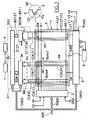
- the memory comprises a two-dimensional array 1 of memory cells, arranged in ( e.g ., 512) rows R0-R511 and ( e.g., 4096) columns C(0;0)-C(127;31). At each intersection between a row and a column, a memory cell MC is provided.
- the memory cells MC are conventionally formed by stacked-gate MOS transistors with a control gate electrode CG connected to the respective row, an electrically insulated floating gate electrode FG, a drain electrode D connected to the respective column, and a source electrode S.
- the memory cells MC are formed inside semiconductor regions 40-4127 (128 in the shown example), doped of a first conductivity type, for example P type, which extend transversally to the rows.
- the doped semiconductor regions 40-4127, each of which spans across all the rows R0-R511, are arranged side by side.
- the doped semiconductor regions 40-4127 which in the following will be also briefly referred to as “stripes", are formed inside a common N type doped semiconductor well 5, which in turn is formed inside a P type semiconductor chip 50.
- the plurality of 4096 columns is thus made up of 128 packets of thirty-two columns each
- a row address decoder and row selection circuit block 2 receives from a bus ADD of address signal lines row address signal lines RADD. Block 2 decodes a digital code carried by the row address signal lines RADD and selects, among the plurality of rows R0-R511, one row corresponding to the digital code, providing the required bias voltage, that depends on the memory operation mode, to both the selected row and the unselected rows.
- a column address decoder and column selection circuit block 3 receives from bus ADD column address signal lines CADD.
- Block 3 comprises a plurality (128 in the shown example) of first-level decoder and selection circuit blocks 30-3127, each one associated with a respective column packet, for selecting for example one group of eight columns (B0-B3)-(B508-B511) among the thirty-two columns of each column packet.
- Block 3 further comprises a second-level decoder and selection circuit block 300 for selecting one group of eight columns B20-B2127 among the 128 groups of eight columns provided at the output of the first-level circuit blocks 30-3127.
- one group of eight columns among the 512 groups of eight columns B0-B511 can be selectively electrically coupled to a sensing circuitry 6 or to a programming circuitry 7.
- the actual number of the groups of columns that can be selected by blocks 30-3127 and 300 only depends on the degree of parallelism of the sensing and programming circuitries. In the above example, it has been assumed that such a degree of parallelism is equal to eight; memories with a degree of parallelism equal to sixteen are also conventional: in such a case the number of columns in each group that can be selected by blocks 30-3127 and 300 will be equal to sixteen instead of eight.
- a stripe address decoder and stripe selection circuit block 8 receives from bus ADD stripe address signal lines SADD. Block 8 decodes a digital code carried by the stripe address signal lines and selects, among the plurality of stripes 40-4127, one stripe corresponding to the digital code, providing the required bias voltages (through bias lines S0-S127), that depends on the memory operation mode, to both the selected stripe and the unselected stripes.
- a circuit block 9 supplies through a bias line NWB the proper bias voltage, also depending on the memory operation mode, to the N type well 5.
- the elemental memory unit the content of which can be modified individually is constituted by a sub-set of (thirty-two, in the shown example) memory cells MC of the set of (4096 in the example) memory cells of a given row R0-R511, said sub-set including the memory cells MC of said row that are formed in a same stripe 40-4127.
- Said sub-set therefore includes the memory cells which belong to columns of a same column packet (C(0;0)-C(0;31))-(C(127;0)-C(127;31)).
- Said elemental memory unit is also referred to as "memory page” or, briefly, "page” P.
- the memory is thus made up of 2 16 pages P, and since each page contains thirty-two memory cells, each memory page has the size of a so-called "long-word".
- the size of the elemental memory units may vary in dependence of the particular embodiment and may, for example, be equal to eight bits (one Byte), to sixteen bits (a word), to sixty-four bits, or even to other sizes as required by the particular application.
- the elemental memory unit can as well include additional bits for implementing fail correction techniques based on Error Correction Codes (ECC), and/or bits, to be used as flags, for implementing security access schemes.
- ECC Error Correction Codes
- Figures 3 and 4 show the page Flash memory of Figure 1 during an erase operation and, respectively, a write operation.
- Figure 3 relates to an erase operation of an elemental memory unit or page Pe formed by memory cells belonging to row R1 and to columns C(1;0)-C(1;31) (the second column packet).
- Block 2 biases row R1 to a voltage V2, for example a negative voltage equal to approximately -8V (erase voltage).
- V2 a negative voltage equal to approximately -8V (erase voltage).
- the other rows R0 and R2-R511 are biased to ground (GND) or to a low positive voltage, e.g. 2V.
- Block 8 biases stripe 41 to a relatively high positive voltage V1, for example 8V.
- the remaining stripes 40 and 42-4127 are biased to a suitably low voltage, for example to ground.
- the source electrode of the memory cells formed inside a given stripe 40-4127 are kept at a potential substantially corresponding to the biasing potential of the respective stripe: the source electrodes of the memory cells inside stripe 41 are biased to voltage V1, those of the cells of the remaining stripes are biased to ground.
- Block 9 biases the N type well 5 to a positive voltage, for example to voltage V1.
- Block 3 leaves all the columns C(0;0)-C(127;31) floating.
- Figure 4 relates to a write operation of a page Pw formed by memory cells belonging to row R2 and to columns C(1;0)-C(1;31) (the second column packet).
- Block 2 biases row R2 to a relatively high positive voltage V6, for example 8V or 9V.
- V6 a relatively high positive voltage
- the remaining rows R0, R1 and R3-R511 are biased to ground.
- Block 8 biases stripe 41 to a voltage V4, for example ground or a slightly negative voltage, such as -1.2V.
- the remaining stripes 40 and 42-4127 are biased to a voltage V3, for example ground or a low positive voltage, such as 2V.
- the source electrodes of the memory cells formed inside stripe 41 are biased to ground, while those of the memory cells formed inside the other stripes 40 and 42-4127 are biased to voltages substantially corresponding to the biasing voltages of the respective stripes, i.e ., V3.
- Block 3 couples the columns of the second column packet, associated with stripe 41, to the programming circuitry 7.
- the voltage to which each column of the selected packet is biased depends on the datum to be written in the corresponding memory cell (logic "1" or "0"), on the technology used for the manufacture of the memory and on specific application. Assuming by mere convention that a logic "0" corresponds to a written memory cell, to store a "0" into a memory cell the memory cell should be written, and the voltage applied to the drain thereof should be in the voltage range 2V to 6V. On the contrary, to store a logic "1” the memory cell should not be written: in this case the corresponding column is left floating.
- Block 9 biases the N type well 5 to a positive voltage V5 equal to or greater than voltage V3 so as to reverse bias the PN junction formed by P stripe 41 and N well 5.
- Voltage V5 can for example be the main supply voltage (Vdd) of the memory as a whole.
- the problem with such a structure is that all the bits of a given memory Byte or word result to be physically adjacent to each other, being formed in a same P type doped semiconductor stripe.
- the bits of the first Byte Byte0 belong to the first eight columns C(0;0)-C(0;7) of the column packet, those of the second Byte to the second eight columns, and so on, the bits of the fourth Byte Byte3 belong to the last eight columns C(0;24)-C(0;31).
- the problem is that, supposing that the memory is designed to have a degree of parallelism of eight, so that eight memory cells can be written simultaneously, when Byte Byte0 is to be written with all "0"s all the first eight memory cells (Byte0) will inject current into the P type stripe 40 (the memory cell's bulk or substrate), and a significant change in the substrate voltage seen by each memory cell takes place.
- the problem is even exacerbated if the memory has a degree of parallelism of sixteen: in this case, it can happen that all the first sixteen memory cells (Byte0 and Byte1) inject current into the P type stripe 40.
- the present invention provides the following solution.
- the thirty-two columns C(0;0)-C(0;31) of memory cells MC formed inside stripe 40 are scrambled so that, considering a memory page P, bits of said memory page which belong to a same Byte are no more adjacent, but always spaced apart of the maximum distance allowed within the stripe.
- the above arrangement which can be achieved by providing a suitable scrambling of the columns of any given column packet at the level of column address decoding and column selection, assures that the memory cells which can be written in parallel, i.e . simultaneously, are spaced apart of the maximum distance possible inside the memory page.
- the memory is designed to work as a Byte-wide device, with memory locations of the dimension of one Byte each, the memory has a degree of parallelism of eight, so that the number of memory cells that can be read or written in parallel is equal to eight.
- the memory cells i.e ., bits Bi(0), Bi(1),...,Bi(7)
- the memory cells making up a given Byte Bi of page P are spaced apart of a distance equal to four times the pitch of the memory cells along the row. This is also the distance between regions of injection of carriers into the substrate.
- the memory is designed to work as a word-wide (sixteen bits) device, with memory locations of the size of two Bytes each, the memory has a degree of parallelism of sixteen, so that the number of memory cells that can be read or written in parallel is equal to sixteen.
- Bytes B0 and B1 make up one of the memory words of the memory page
- Bytes B2 and B3 make up the other memory word.
- the memory cells making up a given memory word of page P are spaced apart of a distance equal to twice the pitch of the memory cells along the row.
- the two words of the memory page are firstly erased, then the memory cells of the first memory word (B0,B1) are written, and then the memory cells of the second memory word (B2,B3) are written.
- the memory device is designed to work as a long-word device, with memory locations of the size of thirty-two bits each, with a degree of parallelism both in reading and in writing of thirty-two memory cells, there will be no changes with respect to the arrangement of Figure 1.
- the present invention is not limited to the case of memory pages of the size of thirty-two bits.
- the memory pages are longer than thirty-two bits, than the scrambling scheme described above shall be propagated so as to keep the memory cells that can be simultaneously written at the maximum distance possible inside the memory page.
- each memory page contains 2 m bits.
- each column packet contains 2 m columns. If 2 n (with n ⁇ m) is the degree of parallelism of the memory device, that is, the number of memory cells that can be written simultaneously, the present invention provides for distributing every 2 (m-n) columns of a column packet those columns of the column packet containing memory cells that, in a write operation, can be written simultaneously.
- the present invention is not limited to cases in which the number of bits contained in a given memory page is a power of two. This typically occurs when fail bit correction is implemented by means of an Error Correction Code (ECC), and/or a security access scheme based on flag bits is used.
- ECC Error Correction Code
- the case be considered of a thirty-two data bit memory page (as the one described before), with capability of correcting one fail bit.
- six additional bits are necessary: the total number of bits of the memory page (data bits plus ECC bits) amounts to thirty-eight.
- the six additional ECC bits belong to six additional columns of the column packet.
- an advantageous scrambling scheme provides for associating columns C(0;32) and C(0;36) to the first Byte B0, columns C(0;33) and C(0;37) to the third Byte B2, column C(0;34) to the second Byte B1 and column C(0;35) to the fourth Byte B3.
- the memory is designed to work as a Byte-wide device (which however in this case means that the programming circuitry 7 is capable of programming simultaneously up to ten memory cells), then again the memory cells making up a given Byte Bi of the memory page are spaced apart of a distance equal to four times the pitch of the memory cells along the row. If instead the memory is designed to work as a word-wide device (which in this case means that the programming circuitry is capable of programming up to nineteen memory cells), then again the memory cells making up the couples of Bytes (B0,B1) and (B2,B3) are spaced apart of a distance equal to twice the pitch of the memory cells along the row.
- the six additional columns can be distributed so that three of them are physically located at one side of the thirty-two columns, and the remaining three are physically located at the other side.
- the writing sequence of a memory page is made up of five phases: four for programming the for Bytes B0-B3, one for programming the six ECC bits.
- three adjacent memory cells at one side and three at the other side of the column packet are simultaneously programmed. This however does not pose great problems, since the two groups of three adjacent memory cells are spaced apart from each other of thirty-two memory cells. Moreover, since the two groups of three memory cells are located near the boundary of the respective stripe 40 (where substrate contacts are provided), no significant problems of voltage drops in the substrate arise.
- the present invention the problem of reduction of writing efficiency due to variation of the memory cells' substrate potential is minimized, since the memory cells that are simultaneously written, and which potentially inject carriers into the substrate (the respective P type stripes) are spaced apart. So, the degree of parallelism of the memory in writing can be kept high.
- the implementation of the present invention does not cause any increase in complexity and area of the column address decoding and column selection - circuits. Moreover, a gain in area can be achieved because the constraints in the substrate bias contact efficiency can be relaxed: the distance between substrate contact regions can thus be increased, and the number of substrate contact regions be reduced.
- FIG 6 an alternative embodiment of the present invention is shown.
- a column address scrambling circuit block 10 is provided in the memory.
- Block 10 is inserted between address input buffers of the memory (the conventional interface circuits through which the address signals of the bus ADD are furnished to the memory device, not shown in the drawing) and the column address decoding and column selection circuit block 3, which in this case are completely similar to those depicted in Figure 1.
- Block 10 which can easily be made up of simple logic gates, performs a transformation of digital code: an input digital code carried by bus CADD, corresponding to the column address of a given memory Byte or word, is transformed into an output digital code forming an internal column address.
- the internal column address, carried by an internal column address signal line bus INT_CADD is such that, when supplied to the column address decoding and column selection circuits, the same scrambling scheme described in relation to the first embodiment is achieved.
- the memory may contain more than one two-array of memory cells, each one forming a memory sector.
- the memory sectors of the memory could have the structure of the two-array 1 previously described.
Landscapes
- Read Only Memory (AREA)
Abstract
Description
characterized by comprising:
| C(0;0) | C(0;1) | C(0;2) | C(0;3) | C(0;4) | C(0;5) | C(0;6) | C(0;7) |
| B0(0) | B2(0) | B1(0) | B3(0) | B0(1) | B2(1) | B1(1) | B3(1) |
| C(0;8) | C(0;9) | C(0;10) | C(0;11) | C(0;12) | C(0;13) | C(0;14) | C(0;15) |
| B0(2) | B2(2) | B1(2) | B3(2) | B0(3) | B2(3) | B1(3) | B3(3) |
| C(0;16) | C(0;17) | C(0;18) | C(0;19) | C(0;20) | C(0;21) | C(0;22) | C(0;23) |
| B0(4) | B2(4) | B1(4) | B3(4) | B0(5) | B2(5) | B1(5) | B3(5) |
| C(0;24) | C(0;25) | C(0;26) | C(0;27) | C(0;28) | C(0;29) | C(0;30) | C(0;31) |
| B0(6) | B2(6) | B1(6) | B3(6) | B0(7) | B2(7) | B1(7) | B3(7) |
| C(0;0) | C(0;1) | C(0;2) | C(0;3) | C(0;4) | C(0;5) | C(0;6) | C(0;7) |
| LW(0) | LW(16) | LW(8) | LW(24) | LW(1) | LW(17) | LW(9) | LW(25) |
| C(0;8) | C(0;9) | C(0;10) | C(0;11) | C(0;12) | C(0;13) | C(0;14) | C(0;15) |
| LW(2) | LW(18) | LW(10) | LW(26) | LW(3) | LW(19) | LW(11) | LW(27) |
| C(0;16) | C(0;17) | C(0;18) | C(0;19) | C(0;20) | C(0;21) | C(0;22) | C(0;23) |
| LW(4) | LW(20) | LW(12) | LW(28) | LW(5) | LW(21) | LW(13) | LW(29) |
| C(0;24) | C(0;25) | C(0;26) | C(0;27) | C(0;28) | C(0;29) | C(0;30) | C(0;31) |
| LW(6) | LW(22) | LW(14) | LW(30) | LW(7) | LW(23) | LW(15) | LW(31) |
Claims (7)
- Non-volatile, electrically alterable semiconductor memory, comprising at least one two-dimensional array of memory cells (MC) with a plurality of rows (R0-R511) and a plurality of columns (C(0;0)-C(127;31)), column selection means (CADD,3;CADD,10,INT_CADD,3) for selecting columns among said plurality of columns, and a write circuit (7) for simultaneously writing a first number of memory cells,
characterized by comprising:a plurality of doped semiconductor regions (40-4127) extending transversally to the rows and subdividing a set of memory cells of each row in a corresponding plurality of subsets of memory cells, each subset of memory cells including memory cells of the row formed in a respective doped semiconductor region distinct from the remaining doped semiconductor regions and defining an elementary memory block (P) that can be individually erased;a plurality of column packets (C(0;0)-C(0;31),...,C(127;0)-C(127;31)) each one containing a second number of columns, said second number being equal to or higher than said first number, memory cells (MC) belonging to columns of a same column packet being formed in a same doped semiconductor region distinct from the doped semiconductor regions in which memory cells belonging to columns of the other column packets are formed,said column selection means being such that, within each column packet, columns containing memory cells that can be written simultaneously by the write circuit are distributed among the columns of the column packet so as to be at the substantially maximum distance from each other allowable within the column packet. - Memory according to Claim 1, further comprising doped semiconductor region selection means (SADD,8), comprising a doped semiconductor region address signal line bus (SADD) and a doped semiconductor region address decoding and selection circuit (8), for selectively supplying to the doped semiconductor regions (40-4127) respective biasing voltages depending on an operation mode of the memory.
- Memory according to Claim 2, further comprising row selection means (RADD,2) for selecting rows among said plurality of rows (R0-R511), capable of selecting one row (R1) during an erase operation, so as to supply a row erase voltage (V2) only to the selected row.
- Memory according to Claim 1, 2 or 3, in which said column selection means (CADD,3) comprise a column address signal line bus (CADD), carrying a digital code defining a column address, column address decoding and column selection circuits (3) receiving the column address and, based thereon, performing a selection of a column packet (C(0;0)-C(0;31)...,C(127;0)-C(127;31)) among said plurality of column packets and a selection of a number of columns equal to said first number within the selected column packet, the selected columns being distributed among the columns of the column packet so as to be at the substantially maximum distance from each other allowable within the column packet.
- Memory according to Claim 1, 2 or 3, in which said column selection means (CADD,10,INT_CADD,3) comprise a column address signal line bus (CADD), carrying a digital code provided from outside to the memory and defining a column address, a digital code transformation circuit (10) for performing a transformation from the digital code provided from the outside into a transformed internal digital code (INT_CADD), column address decoding and column selection circuits (3) receiving the internal digital code and, based thereon, performing a selection of a column packet (C(0;0)-C(0;31)...,C(127;0)-C(127;31)) among said plurality of column packets and a selection of a number of columns equal to said first number within the selected column packet, the transformed digital code being such that the columns selected by the column address decoding and column selection circuits (3) are distributed among the columns of the column packet so as to be at the substantially maximum distance from each other allowable within the column packet.
- Memory according to any one of the preceding claims, in which said first number is equal to 2n, said second number is equal to 2m, (m ≥ n), said column selection means being such that, within each column packet, columns containing memory cells that can be written simultaneously by the write circuit are distributed every 2 (m-n) columns of the column packet.
- Method of writing a memory location (B0-B3) of a memory comprising at least one two-dimensional array of memory cells with a plurality of rows (R0-R511) and a plurality of columns (C(0;0)-C(127;31)), row selection means (RADD,2) for selecting rows among said plurality of rows (R0-R511), column selection means (CADD,3;CADD,10,INT_CADD,3) for selecting columns among said plurality of columns, a write circuit (7) for simultaneously writing a first number of memory cells (MC), a plurality of doped semiconductor regions (40-4127) extending transversally to the rows and subdividing a set of memory cells of each row in a corresponding plurality of subsets of memory cells, each subset of memory cells including memory cells of the row formed in a respective doped semiconductor region distinct from the remaining doped semiconductor regions and defining an elementary memory block (P) that can be individually erased, a plurality of column packets (C(0;0)-C(0;31),...,C(127;0)-C(127;31)) each one containing a second number of columns, said second number being equal to or higher than said first number, memory cells (MC) belonging to columns of a same column packet being formed in a same doped semiconductor region distinct from the doped semiconductor regions in which memory cells belonging to columns of the other column packets are formed, the method providing for:selecting one row (R2) among the plurality of rows;selecting one column packet among the plurality of columns packet; andin the selected column packet, selecting a number of columns equal to said first number containing memory cells that are to be written simultaneously by the write circuit in such a way that the selected columns are distributed among the columns of the column packet so as to be at the substantially maximum distance from each other allowable within the column packet.
Priority Applications (3)
| Application Number | Priority Date | Filing Date | Title |
|---|---|---|---|
| EP01830039A EP1227499B1 (en) | 2001-01-24 | 2001-01-24 | Non-volatile electrically alterable semiconductor memory |
| DE60119483T DE60119483D1 (en) | 2001-01-24 | 2001-01-24 | Non-volatile electrically variable semiconductor memory |
| US10/057,769 US6618315B2 (en) | 2001-01-24 | 2002-01-24 | Non-volatile, electrically alterable semiconductor memory |
Applications Claiming Priority (1)
| Application Number | Priority Date | Filing Date | Title |
|---|---|---|---|
| EP01830039A EP1227499B1 (en) | 2001-01-24 | 2001-01-24 | Non-volatile electrically alterable semiconductor memory |
Publications (2)
| Publication Number | Publication Date |
|---|---|
| EP1227499A1 true EP1227499A1 (en) | 2002-07-31 |
| EP1227499B1 EP1227499B1 (en) | 2006-05-10 |
Family
ID=8184369
Family Applications (1)
| Application Number | Title | Priority Date | Filing Date |
|---|---|---|---|
| EP01830039A Expired - Lifetime EP1227499B1 (en) | 2001-01-24 | 2001-01-24 | Non-volatile electrically alterable semiconductor memory |
Country Status (3)
| Country | Link |
|---|---|
| US (1) | US6618315B2 (en) |
| EP (1) | EP1227499B1 (en) |
| DE (1) | DE60119483D1 (en) |
Cited By (1)
| Publication number | Priority date | Publication date | Assignee | Title |
|---|---|---|---|---|
| US7993957B2 (en) | 2002-02-20 | 2011-08-09 | Micron Technology, Inc. | Phase change memory cell and manufacturing method thereof using minitrenches |
Families Citing this family (2)
| Publication number | Priority date | Publication date | Assignee | Title |
|---|---|---|---|---|
| EP1227499B1 (en) * | 2001-01-24 | 2006-05-10 | STMicroelectronics S.r.l. | Non-volatile electrically alterable semiconductor memory |
| EP1569242A1 (en) * | 2004-02-27 | 2005-08-31 | STMicroelectronics S.r.l. | Electrically word-erasable non-volatile memory-device, and biasing method thereof |
Citations (1)
| Publication number | Priority date | Publication date | Assignee | Title |
|---|---|---|---|---|
| EP0477938A2 (en) * | 1990-09-28 | 1992-04-01 | Kabushiki Kaisha Toshiba | Semiconductor memory device |
Family Cites Families (6)
| Publication number | Priority date | Publication date | Assignee | Title |
|---|---|---|---|---|
| JPH08111096A (en) | 1994-10-12 | 1996-04-30 | Nec Corp | Semiconductor storage device and erasing method therefor |
| TW378330B (en) * | 1997-06-03 | 2000-01-01 | Fujitsu Ltd | Semiconductor memory device |
| US6401167B1 (en) * | 1997-10-10 | 2002-06-04 | Rambus Incorporated | High performance cost optimized memory |
| EP1130517B1 (en) * | 2000-03-02 | 2004-05-26 | STMicroelectronics S.r.l. | Redundancy architecture for an interleaved memory |
| US6304504B1 (en) * | 2000-08-30 | 2001-10-16 | Micron Technology, Inc. | Methods and systems for alternate bitline stress testing |
| EP1227499B1 (en) * | 2001-01-24 | 2006-05-10 | STMicroelectronics S.r.l. | Non-volatile electrically alterable semiconductor memory |
-
2001
- 2001-01-24 EP EP01830039A patent/EP1227499B1/en not_active Expired - Lifetime
- 2001-01-24 DE DE60119483T patent/DE60119483D1/en not_active Expired - Lifetime
-
2002
- 2002-01-24 US US10/057,769 patent/US6618315B2/en not_active Expired - Lifetime
Patent Citations (1)
| Publication number | Priority date | Publication date | Assignee | Title |
|---|---|---|---|---|
| EP0477938A2 (en) * | 1990-09-28 | 1992-04-01 | Kabushiki Kaisha Toshiba | Semiconductor memory device |
Cited By (2)
| Publication number | Priority date | Publication date | Assignee | Title |
|---|---|---|---|---|
| US7993957B2 (en) | 2002-02-20 | 2011-08-09 | Micron Technology, Inc. | Phase change memory cell and manufacturing method thereof using minitrenches |
| US9876166B2 (en) | 2002-02-20 | 2018-01-23 | Micron Technology, Inc. | Phase change memory cell and manufacturing method thereof using minitrenches |
Also Published As
| Publication number | Publication date |
|---|---|
| DE60119483D1 (en) | 2006-06-14 |
| EP1227499B1 (en) | 2006-05-10 |
| US20020154546A1 (en) | 2002-10-24 |
| US6618315B2 (en) | 2003-09-09 |
Similar Documents
| Publication | Publication Date | Title |
|---|---|---|
| US6967896B2 (en) | Address scramble | |
| US7848140B2 (en) | Flash memory array system including a top gate memory cell | |
| US5270980A (en) | Sector erasable flash EEPROM | |
| US5579259A (en) | Low voltage erase of a flash EEPROM system having a common erase electrode for two individually erasable sectors | |
| US8234440B2 (en) | Nonvolatile semiconductor memory device with advanced multi-page program operation | |
| US20040008541A1 (en) | Multiple use memory chip | |
| KR100370909B1 (en) | A 1 chip microcomputer and a data refresh method thereof | |
| EP0640984A2 (en) | Floating gate memory device | |
| US6108236A (en) | Smart card comprising integrated circuitry including EPROM and error check and correction system | |
| KR20080009073A (en) | Nonvolatile Memory and Source Line Bias Errors Compensation Method | |
| US20100177568A1 (en) | Read mode for flash memory | |
| US6865114B2 (en) | Word line selector for a semiconductor memory | |
| KR19990008133A (en) | Nonvolatile Memory Blocking Architecture | |
| US6891755B2 (en) | Architecture for a flash-EEPROM simultaneously readable in other sectors while erasing and/or programming one or more sectors | |
| US20140198571A1 (en) | Selecting memory cells | |
| US6950336B2 (en) | Method and apparatus for emulating an electrically erasable programmable read only memory (EEPROM) using non-volatile floating gate memory cells | |
| KR100639827B1 (en) | 1 transistor cell for EEPROM applications | |
| US20090279361A1 (en) | Addressable Memory Array | |
| US6501684B1 (en) | Integrated circuit having an EEPROM and flash EPROM | |
| EP1227499B1 (en) | Non-volatile electrically alterable semiconductor memory | |
| US6724663B2 (en) | Erase block architecture for non-volatile memory | |
| US12380932B2 (en) | Row decoder and row address scheme in a memory system | |
| US7342830B1 (en) | Program and program verify operations for flash memory | |
| KR950034269A (en) | Nonvolatile Semiconductor Memory Device | |
| US6373742B1 (en) | Two side decoding of a memory array |
Legal Events
| Date | Code | Title | Description |
|---|---|---|---|
| PUAI | Public reference made under article 153(3) epc to a published international application that has entered the european phase |
Free format text: ORIGINAL CODE: 0009012 |
|
| AK | Designated contracting states |
Kind code of ref document: A1 Designated state(s): AT BE CH CY DE DK ES FI FR GB GR IE IT LI LU MC NL PT SE TR |
|
| AX | Request for extension of the european patent |
Free format text: AL;LT;LV;MK;RO;SI |
|
| 17P | Request for examination filed |
Effective date: 20020813 |
|
| AKX | Designation fees paid |
Designated state(s): DE FR GB IT |
|
| GRAP | Despatch of communication of intention to grant a patent |
Free format text: ORIGINAL CODE: EPIDOSNIGR1 |
|
| GRAS | Grant fee paid |
Free format text: ORIGINAL CODE: EPIDOSNIGR3 |
|
| GRAA | (expected) grant |
Free format text: ORIGINAL CODE: 0009210 |
|
| AK | Designated contracting states |
Kind code of ref document: B1 Designated state(s): DE FR GB IT |
|
| PG25 | Lapsed in a contracting state [announced via postgrant information from national office to epo] |
Ref country code: IT Free format text: LAPSE BECAUSE OF FAILURE TO SUBMIT A TRANSLATION OF THE DESCRIPTION OR TO PAY THE FEE WITHIN THE PRE;WARNING: LAPSES OF ITALIAN PATENTS WITH EFFECTIVE DATE BEFORE 2007 MAY HAVE OCCURRED AT ANY TIME BEFORE 2007. THE CORRECT EFFECTIVE DATE MAY BE DIFFERENT FROM THE ONE RECORDED.SCRIBED TIME-LIMIT Effective date: 20060510 |
|
| REG | Reference to a national code |
Ref country code: GB Ref legal event code: FG4D |
|
| REF | Corresponds to: |
Ref document number: 60119483 Country of ref document: DE Date of ref document: 20060614 Kind code of ref document: P |
|
| PG25 | Lapsed in a contracting state [announced via postgrant information from national office to epo] |
Ref country code: DE Free format text: LAPSE BECAUSE OF FAILURE TO SUBMIT A TRANSLATION OF THE DESCRIPTION OR TO PAY THE FEE WITHIN THE PRESCRIBED TIME-LIMIT Effective date: 20060811 |
|
| ET | Fr: translation filed | ||
| PLBE | No opposition filed within time limit |
Free format text: ORIGINAL CODE: 0009261 |
|
| STAA | Information on the status of an ep patent application or granted ep patent |
Free format text: STATUS: NO OPPOSITION FILED WITHIN TIME LIMIT |
|
| 26N | No opposition filed |
Effective date: 20070213 |
|
| PGFP | Annual fee paid to national office [announced via postgrant information from national office to epo] |
Ref country code: IT Payment date: 20080122 Year of fee payment: 8 |
|
| PGFP | Annual fee paid to national office [announced via postgrant information from national office to epo] |
Ref country code: GB Payment date: 20081229 Year of fee payment: 9 |
|
| PGFP | Annual fee paid to national office [announced via postgrant information from national office to epo] |
Ref country code: FR Payment date: 20090128 Year of fee payment: 9 |
|
| GBPC | Gb: european patent ceased through non-payment of renewal fee |
Effective date: 20100124 |
|
| REG | Reference to a national code |
Ref country code: FR Ref legal event code: ST Effective date: 20100930 |
|
| PG25 | Lapsed in a contracting state [announced via postgrant information from national office to epo] |
Ref country code: FR Free format text: LAPSE BECAUSE OF NON-PAYMENT OF DUE FEES Effective date: 20100201 |
|
| PG25 | Lapsed in a contracting state [announced via postgrant information from national office to epo] |
Ref country code: GB Free format text: LAPSE BECAUSE OF NON-PAYMENT OF DUE FEES Effective date: 20100124 |
|
| PG25 | Lapsed in a contracting state [announced via postgrant information from national office to epo] |
Ref country code: IT Free format text: LAPSE BECAUSE OF NON-PAYMENT OF DUE FEES Effective date: 20090124 |