EP1227494A2 - Magnetic random access memory - Google Patents
Magnetic random access memory Download PDFInfo
- Publication number
- EP1227494A2 EP1227494A2 EP01126567A EP01126567A EP1227494A2 EP 1227494 A2 EP1227494 A2 EP 1227494A2 EP 01126567 A EP01126567 A EP 01126567A EP 01126567 A EP01126567 A EP 01126567A EP 1227494 A2 EP1227494 A2 EP 1227494A2
- Authority
- EP
- European Patent Office
- Prior art keywords
- word line
- write word
- wwl0
- bit line
- wwl1
- Prior art date
- Legal status (The legal status is an assumption and is not a legal conclusion. Google has not performed a legal analysis and makes no representation as to the accuracy of the status listed.)
- Granted
Links
Images




Classifications
-
- G—PHYSICS
- G11—INFORMATION STORAGE
- G11C—STATIC STORES
- G11C11/00—Digital stores characterised by the use of particular electric or magnetic storage elements; Storage elements therefor
- G11C11/02—Digital stores characterised by the use of particular electric or magnetic storage elements; Storage elements therefor using magnetic elements
- G11C11/14—Digital stores characterised by the use of particular electric or magnetic storage elements; Storage elements therefor using magnetic elements using thin-film elements
- G11C11/15—Digital stores characterised by the use of particular electric or magnetic storage elements; Storage elements therefor using magnetic elements using thin-film elements using multiple magnetic layers
-
- G—PHYSICS
- G11—INFORMATION STORAGE
- G11C—STATIC STORES
- G11C11/00—Digital stores characterised by the use of particular electric or magnetic storage elements; Storage elements therefor
- G11C11/02—Digital stores characterised by the use of particular electric or magnetic storage elements; Storage elements therefor using magnetic elements
- G11C11/16—Digital stores characterised by the use of particular electric or magnetic storage elements; Storage elements therefor using magnetic elements using elements in which the storage effect is based on magnetic spin effect
- G11C11/165—Auxiliary circuits
- G11C11/1693—Timing circuits or methods
Definitions
- the present invention relates to a magnetic random access memory and, more particularly, to a technique of improving the reliability of a line through which a large current flows in write operation.
- an MRAM to which a GMR (Giant Magneto-Resistance) effect is applied Before the application of the TMR effect to an MRAM, an MRAM to which a GMR (Giant Magneto-Resistance) effect is applied has been known.
- the MR ratio of an MRAM to which the GMR effect is applied is several % to about 10%.
- the MRAM to which the GMR effect is applied uses a technique of canceling out variations in characteristics among a plurality of magneto-resistance elements (memory cells) to prevent a data read error due to a very low signal level.
- magneto-resistance elements memory cells
- data read operation is performed twice with respect to a single memory cell to prevent the effect of variation in characteristics among magneto-resistance elements. It is therefore difficult to realize high-speed read operation in the MRAM to which the GMR effect is applied.
- a memory cell When a memory cell is comprised of a GMR element and a MOS transistor as a switch, if the ON resistance of the MOS transistor is not sufficiently low, a signal (cell data) read out from the memory cell may be lost due to the influence of variations in the characteristics of MOS transistor.
- the ON resistance of the MOS transistor in the memory cell may be decreased to a value almost equal to that of the GMR element.
- the MOS transistor needs to have a considerably large size. This makes it difficult to attain a large memory capacity by decreasing the memory cell size.
- the GMR and MRAM are used only under special environments, e.g., in space, owing to their characteristic feature, i.e., having excellent radiation resistance, but are not generally used much.
- the basic structure of a TMR element is the MTJ structure in which an insulating film is sandwiched between two ferromagnetic layers.
- a magnetic member has a direction in which magnetization tends to be oriented, i.e., a magnetization easy axis.
- the magnetization easy axis direction is the direction in which the internal energy in the magnetic layer is minimized when the direction coincides with the magnetization direction. If, therefore, no external magnetic field is applied, the magnetization of the ferromagnetic layer of the TMR element is oriented in the magnetization easy axis direction, and the relative directions of the magnetization of the two ferromagnetic layers are set in two different states, i.e., parallel and anti-parallel.
- the TMR element changes in resistance depending on whether the magnetization directions of the two ferromagnetic layers are parallel or anti-parallel. It is generally assumed that this change is based on the spin dependence of tunneling probability.
- binary data can be stored depending on whether the magnetization directions of the ferromagnetic layers of the TMR element are parallel or anti-parallel.
- cell data can be read out by using a change in the resistance of the TMR element due to a magnetization state.
- the MR ratio of an MRAM using the TMR effect is several ten %, and a resistance value for the TMR element can be selected from a wide range of resistance values by changing the thickness of the insulating layer (tunnel insulating film) sandwiched between the two magnetic layers.
- the signal level in read operation may become equal to or more than the signal level in the DRAM.
- write operation is performed by changing the magnetization direction of the TMR element (making it parallel or anti-parallel) using the magnetic field generated by currents flowing in two lines (line word line and bit line) perpendicular to each other.
- the relative directions of magnetization of the two ferromagnetic layers can be made parallel or anti-parallel by arbitrarily reversing only the magnetization of the thinner magnetic layer (having lower coercive force).
- the relative directions of magnetization of the two ferromagnetic layers can be made parallel or anti-parallel by arbitrarily reversing only the magnetization of the magnetic layer to which the diamagnetic layer is not added.
- a magnetic layer has the following property. Assume that the magnetization of the magnetic layer is to be reversed by applying a magnetic field in a direction opposite to the magnetization direction of the magnetic layer. In this case, if a magnetic field is applied in advance in a direction perpendicular to the magnetization direction, the magnitude of a magnetic field (reversing magnetic field) required to reverse the magnetization of the magnetic layer can be reduced.
- FIG. 1 shows an asteroid curve
- the asteroid curve represents the magnitude of a magnetic field whose magnetization is reversed when a magnetic field parallel to the magnetization easy axis direction and a magnetic field perpendicular to the magnetization easy axis direction are applied at once.
- the magnetization easy axis direction is the x direction.
- the three vectors shown in FIG. 1 represent the vectors of magnetic fields generated in the first memory cell area located at the intersection of two lines through which write currents flow and the second memory area adjacent to the first memory cell area.
- a reversed magnetic field has the property of increasing in inverse proportion to the width of a magnetic member.
- the width of the magnetic member decreases, and the reversed magnetic field must be increased. As a result, a larger current is required to generate a reversed magnetic field.
- the line width decreases, and hence the current density abruptly increases.
- an electromigration (EM) phenomenon tends to occur due to a large current required to generate a reversed magnetic field, resulting in a deterioration in line reliability.
- the attenuation ratio of a magnetic field at a line adjacent to a line in which a large current flows decreases. This means that the interference of a write magnetic field with the adjacent cell (unselected cell) increases. That is, since reversed magnetic fields vary depending on memory cells, if the line thickness increases, the probability of write errors with respect to unselected cells increases.
- a magnetic random access memory comprising a write word line, a bit line crossing the write word line, a magneto-resistance element which is placed at an intersection of the write word line and the bit line and stores data in accordance with a direction of magnetization that changes depending on a magnetic field generated by a current flowing in the write word line and a current flowing in the bit line, and a driver for causing the magneto-resistance element to store data by making a current flow in the write word line in a first direction, and then making a current flow in the write word line in a second direction.
- a magnetic random access memory according to an aspect of the present invention will be described in detail below with reference to the views of the accompanying drawing.
- currents are respectively supplied to a write word line and bit line in directions opposite to the directions of currents that flowed in the write operation.
- the current values of these currents flowing in the opposite directions are equal to those of the currents that flowed in the write operation.
- the period during which a current is supplied to the write word line in the opposite direction is shifted from the period during which a current is supplied to the bit line in the opposite direction so as not to change the magnetization of a magneto-resistance element.
- the direction of a current flowing in the write word line does not depend on the magnetization direction (the value of data to be written in the memory cell), and hence can be changed for every write cycle.
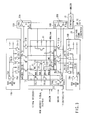
- FIG. 2 shows the main part of a magnetic random access memory according to the first embodiment of the present invention.
- a row decoder 12 is placed on an end portion of a memory cell array 11 in the row direction.
- a row address signal RA0-RAn is input to the row decoder 12.
- the row decoder 12 is activated when a write word line enable signal WWLEN or read word line enable signal RWLEN is enabled.
- the row decoder 12 selects a write word line (row) WWL of the memory cell array 11 on the basis of the row address signal RA0-RAn.
- the write word line WWL and a bit line BL serve to make the magnetization directions of the two magnetic layers of a memory cell parallel or anti-parallel.
- a WWL driver 13 drives the selected write word line WWL.
- a controller 17 is activated when the write word line enable signal WWLEN is enabled.
- the controller 17 is formed by, for example, a reset down trigger D-FF (Delay Flip-Flop) circuit and is made to function as a 1-bit counter by feeding back an inverted output to the input terminal.
- D-FF Delay Flip-Flop
- the state of the reset down trigger D-FF circuit is determined in an initialization stage by a reset signal. For example, an output D of the reset down trigger D-FF circuit is inverted every time the write word line enable signal WWLEN falls.
- An output signal from the reset down trigger D-FF circuit is supplied to the WWL driver 13.
- the row decoder 12 selects a read word line (row) RWL of the memory cell array 11 on the basis of the row address signal RA0-RAn.
- the read word line RWL serves to turn on a MOS transistor (switch) as an element of the selected memory cell in read operation.
- a column address signal CA0-CAm is input to a column decoder 14.
- the column decoder 14 decodes the column address signal CA0-CAm and outputs column select signals CSL0, CSL1, ⁇ .
- the column select signals CSL0, CSL1, ⁇ are further input to bit line selectors 19A and 19B.
- a write enable signal WE and the least significant bit RA0 of the row address signal RA0-RAn are input to the bit line selectors 19A and 19B.
- the bit line selectors 19A and 19B are activated when write operation is performed, i.e., the write enable signal WE is enabled.
- bit line selectors 19A and 19B select a bit line on the basis of the least significant bit RA0 of the row address signal. This operation is performed because memory cells are laid out in a checkered pattern.
- Output signals from the bit line selectors 19A and 19B are input to write current drivers 16A and 16B.
- the write current drivers 16A and 16B drive the selected bit line BL on the basis of the output signals from the bit line selectors 19A and 19B.
- the direction in which a current flows in the bit line BL is controlled by a controller 18.
- the write word line enable signal WWLEN and write data DATA are input to the controller 18.
- the controller 18 controls the direction of a current flowing in the bit line BL on the basis of the value (binary value) of the write data DATA.
- the controller 18 is formed by a reset down trigger D-FF (Delay Flip-Flop) circuit and is made to function as a 1-bit counter by feeding back an inverted output to the input terminal.
- D-FF Delay Flip-Flop
- the state of the reset down trigger D-FF circuit is determined by a reset signal in an initialization stage. For example, an output D of the reset down trigger D-FF circuit is inverted every time the write word line enable signal WWLEN falls.
- the controller 18 has a multiplexer MUX and changes the direction of a current flowing in the bit line BL by switching two outputs D and /D in accordance with the value of the write data DATA.
- FIG. 3 shows a concrete example of the circuit arrangement of the magnetic random access memory in FIG. 2.
- FIG. 3 an illustration of a sense amplifier and column decoder for read operation is omitted.
- the memory cell array 11 is comprised of a plurality of memory cells MC arranged in the form of an array.
- the memory cell MC is constituted by a TMR element 21 having an insulating layer sandwiched between two magnetic layers and a switch element 22 formed by a MOS transistor.
- One terminal of the TMR element 21 is connected to bit lines BL0, bBL0, BL1, bBL1, ⁇ , and the TMR element 21 and switch element 22 are connected in series with each other between the bit lines BL0, bBL0, BL1, bBL1, ⁇ and a ground point.
- the row decoder 12 is arranged on an end portion of the memory cell array 11 in the row direction.
- the row decoder 12 is prepared for each row.
- the row decoder 12 is comprised of a NAND circuit 23 to which the row address signal RA0-RAn is input, a NOR circuit 24 to which the read word line enable signal RWLEN and inverted signal bRWLEN are input, and a NOR circuit 25 to which an inverted signal bWWLEN of the write word line enable signal WWLEN is input.
- the read word line enable signal RWLEN is kept at "L” level (e.g., the ground potential), and the inverted signal bRWLEN of the read word line enable signal RWLEN is kept at "H” level. Therefore, an output signal RWL from the NOR circuit 24 is always kept at "L” level.
- the write word line enable signal WWLEN is always kept at "L” level (e.g., the ground potential), and the inverted signal bWWLEN of the write word line enable signal WWLEN is always kept at "H” level. Therefore, the output signal RWL from the NOR circuit 25 is always kept at "L” level.
- the WWL driver 13 is comprised of an inverter circuit 26 and an N-channel MOS transistor 27 serving as a transfer gate.
- the inverter circuit 26 outputs a write word line driver signal WWLDRV on the basis of an output signal from the controller 17.
- the write word line driver signal WWLDRV is transferred to write word lines WWL0, WWL1, ⁇ through the N-channel MOS transistor 27.
- Output signals RSL0, RSL1, ⁇ from the row decoder 12 are input to the gate of the N-channel MOS transistor 27 serving as a transfer gate. Since only the transfer gate of the row selected by the row address signal RA0-RAn is set in the ON state, the WWL driver 13 drives only the selected write word line WWL.
- the row decoder 12 sets the output signal (decode signal) RSL1 at "H" level. In write operation, therefore, the WWL driver 13 controls the direction of a current flowing in the write word line WWL1.
- the controller 17 is comprised of a reset down trigger D-FF (Delay Flip-Flop) circuit.
- This D-FF circuit has an inverted output fed back to the input terminal and functions as a 1-bit counter.
- the state of the D-FF circuit is determined by a reset signal in an initialization stage.
- an output signal D from the D-FF circuit is inverted every time the write word line enable signal WWLEN falls.
- the read word lines RWL0, RWL1, ⁇ are used to turn on the MOS transistor (switch) 22 as an element of the selected memory cell MC in read operation.
- the row decoder 12 selects a row (read word line RWL) of the memory cell array 11 on the basis of the row address signal RA0-RAn.
- the bit line selectors 19A and 19B are comprised of NAND circuits 28A and 28B and NOR circuits 29-00, 29-01, 29-10, 29-11, ⁇ .
- the column select signals CSL0, CSL1, ⁇ obtained by decoding the column address signal CA0-CAm are input to the NOR circuits 29-00, 29-01, 29-10, 29-11, ⁇ .
- the write enable signal WE is set at "H” level, and for example, one of the column select signals CSL0, CSL1, ⁇ is set at "H” level.
- the bit line selectors 19A and 19B select a bit line on the basis of the least significant bit RA0 of the row address signal.
- the write current drivers 16A and 16B are comprised of inverter circuits 30A and 30B and N-channel MOS transistors 31A and 31B serving as transfer gates.
- the inverter circuits 30A and 30B output bit line drive signals BLDRV and bBLDRV on the basis of an output signal from the controller 18.
- the bit line drive signals BLDRV and bBLDRV are transferred to the bit lines BL0, bBL0, BL1, and bBL1 through the N-channel MOS transistors 31A and 31B.
- Output signals from the bit line selectors 19A and 19B are input to the gates of the N-channel MOS transistors 31A and 31B serving as transfer gates. Therefore, only the transfer gate of the column selected by the column address signal CA0-CAm and the least significant bit RA0 of the row address signal is turned on. As a consequence, the write current drivers 16A and 16B drive only the selected bit line BL.
- bit line BL0 is selected by the column address signal CA0-CAm and the least significant bit RA0
- an output signal (decode signal) from the NOR circuit 29-00 in each of the bit line selectors 19A and 19B is set at "H" level. In write operation, therefore, the direction of a current flowing in the bit line BL0 is controlled by the write current drivers 16A and 16B.
- the controller 18 is formed by a reset down trigger D-FF (Delay Flip-Flop) circuit.
- This D-FF circuit has an inverted output fed back to the input terminal and functions as a 1-bit counter.
- the state of the D-FF circuit is determined by a reset signal in an initialization stage.
- the output signal D from the D-FF circuit is inverted every time the write word line enable signal WWLEN falls.
- FIG. 3 A characteristic feature of the operation of the magnetic random access memory (FIG. 3) according to an aspect of the present invention will be described next with reference to FIG. 9.
- the ordinates of signals IWWL0 and IBL0 represent currents, and the ordinates of the remaining signals represent voltages.
- the present operation is characterized in write operation.
- the write enable signal WE is set at "H” level, and the memory enters into the write mode.
- the write word line enable signal WWLEN is set at “H” level
- the column select signal CSL0 is set “H” level
- the remaining column select signals CSL1, ⁇ are maintained at “L” level.
- the output signal RSL0 from the row decoder 12 is set at "H” level to turn on the N-channel MOS transistor (transfer gate) 27 connected to the write word line WWL0.
- the output signals RSL1, ⁇ from the row decoder 12 are set at "L” level, and hence the N-channel MOS transistors (transfer gates) 27 connected to unselected write word lines WWL1, ⁇ are turned off.
- the output signals RWL0, RWL1, ⁇ from the row decoder 12 are set at "L” level, the N-channel MOS transistor 22 in the memory cell MC is also turned off.
- An output signal from the controller 17 is at "L” level, and the write word line driver signal WWLDRV is at "H” level (e.g., Vdd).
- a signal VWWLterm is at a predetermined level (a predetermined value between "H” and “L” of WWLDRV).
- the N-channel MOS transistors (transfer gates) 31A and 31B connected to the bit line BL0 are turned on.
- bit line driver signal BLDRV is set at "H” level (e.g., Vdd)
- bit line driver signal bBLDRV is set at "L” level (e.g., Vss).
- a current flows in the bit line BL0 from the write current driver 30B to the write current driver 30A (this direction of a current is assumed to be a positive direction).
- bit line driver signal BLDRV is set at "L” level (e.g., Vss)
- bit line driver signal bBLDRV is set at "H” level (e.g., Vdd).
- the magnetic field generated by the current IWWL0 flowing in the write word line WWL0 and the current IBL0 flowing in the bit line BL0 is changed in accordance with the direction of the current IBL0 flowing in the bit line BL0, thereby writing write data in the memory cell MC at the intersection of the write word line WWL0 an the bit line BL0.
- the write word line driver signal WWLDRV is therefore set at "L" level, and the current IWWL0 flowing in the write word line WWL0 is stopped.
- the write data DATA is assumed to be at "1". For this reason, as indicated by the timing chart of FIG. 9, a current flows in the bit line BL0 in the positive direction during the execution of write operation. After the write operation is complete, a current flows in the bit line BL0 in the negative direction.
- a current flows in the selected bit line BL0 in a direction opposite to the direction of a current flowing in the bit line BL0 during the execution of data write operation.
- the level of the column select signal CSL0 changes from “H” level to “L” level.
- the N-channel MOS transistor (transfer gate) connected to the bit line BL0 is turned off to stop the reverse current.
- the level (e.g., the fixed value) of the signal VWWLterm is controlled by the voltage down converter 20 to keep the current value of IWWL0 constant regardless of the direction of IWLL0.
- the write word line driver signal WWLDRV is set at "H” level
- the bit line driver signals BLDRV and bBLDRV are set at "H” level and "L” level, respectively, thus restoring the initial state.
- the pulse width of a pulse signal supplied to the write word line WWL0 and bit line BL0 in write operation is substantially equal to the pulse width of a pulse signal supplied to the write word line WWL0 and bit line BL0 when a reverse current is made to flow.
- the pulse width of a pulse signal in supplying a reverse current may be smaller than the pulse width of a pulse signal in write operation.
- a magnetic random access memory is capable of randomly writing data in an arbitrary bit in the memory cell array.
- MRAM magnetic random access memory
- a technique of increasing the write bandwidth for example, a technique of fixing a row address, and writing data in memory cells exiting at the intersections of the row designated by the row address and a plurality of columns is known.
- write operation is not simultaneously performed for all columns, and, for example, column select signals CSLi for selecting columns are sequentially input with time shifts to execute data write operation for memory cells column by column.
- FIG. 11 shows a concrete example of currents flowing in a write word line and bit line during write operation.
- the ordinates of signals IWWL0 and IBL0 represent currents, and the ordinates of the remaining signals represent voltages.
- a write enable signal WE is set at "H” level, and the memory enters into the write mode.
- a write word line enable signal WWLEN is set at "H” level
- a column select signal CSL0 is set “H” level
- the remaining column select signals CSL1, ⁇ are maintained at “L” level.
- an output signal RSL0 from the row decoder 12 is set at "H” level to turn on an N-channel MOS transistor (transfer gate) 27 connected to the write word line WWL0.
- output signals RSL1, ⁇ from the row decoder 12 are set at "L” level, and hence an N-channel MOS transistors (transfer gates) 27 connected to unselected write word lines WWL1, ⁇ are turned off.
- output signals RWL0, RWL1, ⁇ from the row decoder 12 are set at "L” level, an N-channel MOS transistor 22 in the memory cell MC is also turned off.
- An output signal from a controller 17 is at "L” level, and a write word line driver signal WWLDRV is at "H” level (e.g., Vdd).
- a signal VWWLterm is at a predetermined level (a predetermined value between "H” and “L” of WWLDRV).
- N-channel MOS transistors (transfer gates) 31A and 31B connected to the bit line BL0 are turned on.
- bit line driver signal BLDRV is set at "H” level (e.g., Vdd)
- bit line driver signal bBLDRV is set at "L” level (e.g., Vss).
- a current flows in the bit line BL0 from a write current driver 30B to a write current driver 30A (this direction of a current is assumed to be a positive direction).
- bit line driver signal BLDRV is set at "L” level (e.g., Vss)
- bit line driver signal bBLDRV is set at "H” level (e.g., Vdd).
- the magnetic field generated by the current IWWL0 flowing in the write word line WWL0 and the current IBL0 flowing in the bit line BL0 is changed in accordance with the direction of the current IBL0 flowing in the bit line BL0, thereby writing write data in the memory cell MC at the intersection of the write word line WWL0 an the bit line BL0.
- a current flows in the bit line BL0 in the positive direction during the execution of write operation. After the write operation is complete, a current flows in the bit line BL0 in the negative direction.
- a current flows in the selected bit line BL0 in a direction opposite to the direction of a current flowing in the bit line BL0 during the execution of data write operation.
- the level of the column select signal CSL0 changes from “H” level to “L” level.
- the N-channel MOS transistor (transfer gate) connected to the bit line BL0 is turned off to stop the reverse current.
- the case shown in FIG. 11 differs from the case shown in FIG. 9 in the following point.
- the case shown in FIG. 9 while such a current in the negative direction flows in the write word line WWL0, no write operation is performed.
- write operation is performed for the memory cells on the next column (CSL1).
- bit line driver signal BLDRV is set at "H” level (e.g., Vdd).
- bit line driver signal bBLDRV is set at "L” level (e.g., Vss).
- the output signal from the controller 18 is set at "H” level.
- the bit line driver signal BLDRV is set at "L” level (e.g., Vss)
- the bit line driver signal bBLDRV is set at "H” level (e.g., Vdd).
- the magnetic field generated by the current IWWL0 flowing in the write word line WWL0 and the current IBL1 flowing in the bit line BL1 is changed in accordance with the direction of the current IBL1 flowing in the bit line BL1, thereby writing write data in the memory cell MC at the intersection of the write word line WWL0 an the bit line BL1.
- the direction of a current flowing in a write word line in write operation for a memory cell on the column CSL0 differs from the direction of a current flowing in a write word line in write operation for a memory cell on the column CSL1.
- the direction of a current flowing in a write word line is irrelevant to inversion of the magnetization of a memory cell. That is, magnetic field components in a direction perpendicular to the magnetization easy axis direction in magnetization reversal may be generated in either the positive direction or the negative direction. For this reason, no problem arises even if the directions of currents flowing in write word lines in write operation for memory cells on the respective columns CSL0, CSL1, ⁇ differ from each other.
- the write word line enable signal WWLEN changes from “L” level to "H” level again.
- the write word line driver signal WWLDRV is at "H” level, a current flows in the write word line WWL0 from the WWL driver 13 to the voltage down converter 20 (positive direction).
- a current IBL2 in a direction corresponding to the write data DATA flows in the bit line BL2 of the column CSL2 to execute data write for the memory cell MC existing at the interconnection of the write word line WWL0 and the bit line BL2.
- write operation is executed for the memory cell MC on the column CSL3.
- the level (e.g., the fixed value) of the signal VWWLterm is controlled by the voltage down converter 20 to keep the current value of IWWL0 constant regardless of the direction of IWLL0, as indicated by, for example, the timing chart of FIG. 11.
Landscapes
- Engineering & Computer Science (AREA)
- Computer Hardware Design (AREA)
- Mram Or Spin Memory Techniques (AREA)
- Hall/Mr Elements (AREA)
- Semiconductor Memories (AREA)
Abstract
Description
Claims (20)
- A magnetic random access memory comprising:characterized by comprisinga write word line (WWL0, WWL1) ;a bit line (BL0, bBL0, BL1, bBL1) crossing said write word line; anda magneto-resistance element (21) which is placed at an intersection of said write word line (WWL0, WWL1) and said bit line (BL0, bBL0, BL1, bBL1) and stores data in accordance with a direction of magnetization that changes depending on a magnetic field generated by a current flowing in said write word line and a current flowing in said bit line,a driver (31) for causing said magneto-resistance element (21) to store data by making a current flow in said write word line (WWL0, WWL1) in a first direction, and then making a current flow in said write word line (WWL0, WWL1) in a second direction opposite to the first direction.
- The memory according to claim 1, characterized in that while the current flows in said write word line (WWL0, WWL1) in the second direction, the current flowing in said bit line (BL0, bBL0, BL1, bBL1) is interrupted.
- The memory according to claim 1, characterized in that a current value of the current flowing in said write word line (WWL0, WWL1) in the first direction is equal to a current value of the current flowing in said write word line (WWL0, WWL1) in the second direction.
- The memory according to claim 1, characterized in that a direction of the current flowing in said write word line (WWL0, WWL1) is controlled by fixing a potential of one end of said write word line (WWL0, WWL1) and changing a potential of the other end of said write word line (WWL0, WWL1).
- A magnetic random access memory comprising:characterized by comprisinga write word line (WWL0, WWL1);a bit line (BL0, bBL0, BL1, bBL1) crossing said write word line; anda magneto-resistance element (21) which is placed at an intersection of said write word line (WWL0, WWL1) and said bit line (BL0, bBL0, BL1, bBL1) and stores data in accordance with a direction of magnetization that changes depending on a magnetic field generated by a current flowing in said write word line and a current flowing in said bit line,a driver (16A, 16B) for causing said magneto-resistance element (21) to store data by making a current flow in said bit line (BL0, bBL0, BL1, bBL1) in a first direction, and then making a current flow in said bit line (BL0, bBL0, BL1, bBL1) in a second direction opposite to the first direction.
- The memory according to claim 5, characterized in that while the current flows in said bit line (BL0, bBL0, BL1, bBL1) in the second direction, the current flowing in said write word line (WWL0, WWL1) is interrupted.
- The memory according to claim 5, characterized in that a current value of the current flowing in said bit line (BL0, bBL0, BL1, bBL1) in the first direction is equal to a current value of the current flowing in said bit line (BL0, bBL0, BL1, bBL1) in the second direction.
- The memory according to claim 5, characterized in that a direction of the current flowing in said bit line (BL0, bBL0, BL1, bBL1) is controlled by changing potentials of two ends of said bit line (BL0, bBL0, BL1, bBL1).
- A magnetic random access memory comprising:characterized by comprisinga write word line (WWL0, WWL1) ;a bit line (BL0, bBL0, BL1, bBL1) crossing said write word line; anda magneto-resistance element (21) which is placed at an intersection of said write word line (WWL0, WWL1) and said bit line (BL0, bBL0, BL1, bBL1) and stores data in accordance with a direction of magnetization that changes depending on a magnetic field generated by a current flowing in said write word line and a current flowing in said bit line,wherein a period during which the current flows in said write word line (WWL0, WWL1) in the third direction is completely shifted in time from a period during which the current flows in said bit line (BL0, bBL0, BL1, bBL1) in the fourth direction.a driver (13, 16A, 16B) for causing said magneto-resistance element (21) to store data by making a current flow in said write word line (WWL0, WWL1) in a first direction and making a current flow in said bit line (BL0, bBL0, BL1, bBL1) in a second direction, and then making a current flow in said write word line (WWL0, WWL1) in a third direction opposite to the first direction and making a current flow in said bit line (BL0, bBL0, BL1, bBL1) in a fourth direction opposite to the second direction,
- The memory according to claim 9, characterized in that a current value of the current flowing in said write word line (WWL0, WWL1) in the first direction is equal to a current value of the current flowing in said write word line (WWL0, WWL1) in the third direction, and a current value of the current flowing in said bit line (BL0, bBL0, BL1, bBL1) in the second direction is equal to a current value of the current flowing in said bit line (BL0, bBL0, BL1, bBL1) in the fourth direction.
- The memory according to claim 9, characterized in that a direction of the current flowing in said write word line (WWL0, WWL1) is determined by changing a potential of at least one of two end portions of said write word line (WWL0, WWL1), and a direction of the current flowing in said bit line (BL0, bBL0, BL1, bBL1) is determined by changing a potential of at least one of two end portions of said bit line (BL0, bBL0, BL1, bBL1).
- A magnetic random access memory comprising:characterized by comprisinga write word line (WWL0, WWL1) ;bit lines (BL0, bBL0, BL1, bBL1) crossing said write word line; andmagneto-resistance elements (21) which are placed one by one at intersections of said write word line (WWL0, WWL1) and said bit lines (BL0, bBL0, BL1, bBL1) and store data in accordance with directions of magnetization that change depending on magnetic fields generated by a current flowing in said write word line and currents flowing in said bit lines,wherein a period during which the current flows in said write word line (WWL0, WWL1) in the third direction is completely shifted in time from a period during which the current flows in said selected bit line (BL0, bBL0, BL1, bBL1) in the fourth direction.a driver for causing said magneto-resistance element (21) located at an intersection of said write word line (WWL0, WWL1) and a selected bit line of said bit lines (BL0, bBL0, BL1, bBL1) to store data by making a current flow in said write word line in a first direction and making a current flow in said selected bit line in a second direction, and then making a current flow in said write word line (WWL0, WWL1) in a third direction opposite to the first direction and making a current flow in said selected bit line (BL0, bBL0, BL1, bBL1) in a fourth direction opposite to the second direction,
- The memory according to claim 12,
characterized in that data write operation is completed for said magneto-resistance element (21) located at the intersection of said write word line (WWL0, WWL1) and said selected bit line (BL0, bBL0, BL1, bBL1) in one write cycle, and a direction of the current flowing in said write word line (WWL0, WWL1) is changed for each write cycle. - The memory according to claim 12,
characterized in that A memory according to claim 12,
characterized in that data write operation is completed for said magneto-resistance element (21) located at the intersection of said write word line (WWL0, WWL1) and said selected bit line (BL0, bBL0, BL1, bBL1) in one write cycle, and a direction of the current flowing in said selected bit line (BL0, bBL0, BL1, bBL1) is changed once within one write cycle. - The memory according to claim 12,
characterized in that data to be written in said magneto-resistance element (21) located at the intersection of said write word line (WWL0, WWL1) and said selected bit line (BL0, bBL0, BL1, bBL1) is determined by a direction of the current flowing in said selected bit line. - A magnetic random access memory comprising:characterized by comprisinga write word line (WWL0, WWL1);bit lines (BL0, bBL0, BL1, bBL1) crossing said write word line; andmagneto-resistance elements (21) which are placed one by one at intersections of said write word line (WWL0, WWL1) and said bit lines (BL0, bBL0, BL1, bBL1) and store data in accordance with directions of magnetization that change depending on magnetic fields generated by a current flowing in said write word line and currents flowing in said bit lines,wherein a current is made to flow in a second bit line different from said selected first bit line in a period during which the current flows in said write word line (WWL0, WWL1) in the second direction, thereby causing said magneto-resistance element (21) located at an intersection of said write word line (WWL0, WWL1) and said second bit line to store data.a driver (13, 16A, 16B) for causing said magneto-resistance element (21) located at an intersection of said write word line (WWL0, WWL1) and a selected first bit line of said bit lines (BL0, bBL0, BL1, bBL1) to store data by making a current flow in said write word line in a first direction and making a current flow in said selected first bit line, and then making a current flow in said write word line (WWL0, WWL1) in a second direction opposite to the first direction,
- The memory according to claim 16, characterized in that data write operation is completed for said magneto-resistance element (21) located at the intersection of said write word line (WWL0, WWL1) and said first or second bit line in one write cycle, and a direction of the current flowing in said write word line (WWL0, WWL1) is changed for each write cycle.
- The memory according to claim 16,
characterized in that A memory according to claim 12,
characterized in that data write operation is completed for said magneto-resistance element (21) located at the intersection of said write word line (WWL0, WWL1) and said first or second bit line in one write cycle, and a direction of the current flowing in said first or second bit line is changed once within one write cycle. - The memory according to claim 16,
characterized in that data to be written in said magneto-resistance element (21) located at the intersection of said write word line (WWL0, WWL1) and said first or second bit line is determined by a direction of the current flowing in said selected bit line. - The memory according to claim 1, 5, 9, 12, or 16, characterized in that said magneto-resistance element (21) has a structure in which an insulating layer is sandwiched between two magnetic layers.
Applications Claiming Priority (2)
| Application Number | Priority Date | Filing Date | Title |
|---|---|---|---|
| JP2000393200 | 2000-12-25 | ||
| JP2000393200A JP3920564B2 (en) | 2000-12-25 | 2000-12-25 | Magnetic random access memory |
Publications (3)
| Publication Number | Publication Date |
|---|---|
| EP1227494A2 true EP1227494A2 (en) | 2002-07-31 |
| EP1227494A3 EP1227494A3 (en) | 2003-03-19 |
| EP1227494B1 EP1227494B1 (en) | 2008-10-15 |
Family
ID=18859053
Family Applications (1)
| Application Number | Title | Priority Date | Filing Date |
|---|---|---|---|
| EP01126567A Expired - Lifetime EP1227494B1 (en) | 2000-12-25 | 2001-11-15 | Magnetic random access memory |
Country Status (7)
| Country | Link |
|---|---|
| US (1) | US6693822B2 (en) |
| EP (1) | EP1227494B1 (en) |
| JP (1) | JP3920564B2 (en) |
| KR (1) | KR100428596B1 (en) |
| CN (1) | CN1206656C (en) |
| DE (1) | DE60136155D1 (en) |
| TW (1) | TW508827B (en) |
Cited By (3)
| Publication number | Priority date | Publication date | Assignee | Title |
|---|---|---|---|---|
| EP1326253A3 (en) * | 2001-12-17 | 2004-01-02 | NEC Electronics Corporation | Nonvolatile storage device and operating method thereof |
| CN100375193C (en) * | 2002-08-20 | 2008-03-12 | 富士通株式会社 | semiconductor memory |
| CN102165530A (en) * | 2008-09-24 | 2011-08-24 | 高通股份有限公司 | Reducing spin-pump-induced damping of the free layer of a memory device |
Families Citing this family (43)
| Publication number | Priority date | Publication date | Assignee | Title |
|---|---|---|---|---|
| DE10123593C2 (en) * | 2001-05-15 | 2003-03-27 | Infineon Technologies Ag | Magnetic storage device |
| JP2003091987A (en) * | 2001-09-18 | 2003-03-28 | Sony Corp | Magnetic memory device and recording control method thereof |
| US7020008B2 (en) * | 2001-12-26 | 2006-03-28 | Renesas Technology Corp. | Thin film magnetic memory device writing data with bidirectional current |
| JP3778100B2 (en) | 2002-02-08 | 2006-05-24 | ソニー株式会社 | Magnetic memory device using ferromagnetic tunnel junction element |
| JP3808799B2 (en) | 2002-05-15 | 2006-08-16 | 株式会社東芝 | Magnetic random access memory |
| JP3788964B2 (en) * | 2002-09-10 | 2006-06-21 | 株式会社東芝 | Magnetic random access memory |
| JP4131923B2 (en) * | 2002-09-25 | 2008-08-13 | 株式会社東芝 | Magnetic random access memory |
| US6909630B2 (en) | 2002-12-09 | 2005-06-21 | Applied Spintronics Technology, Inc. | MRAM memories utilizing magnetic write lines |
| US6870759B2 (en) * | 2002-12-09 | 2005-03-22 | Applied Spintronics Technology, Inc. | MRAM array with segmented magnetic write lines |
| KR100506060B1 (en) * | 2002-12-16 | 2005-08-05 | 주식회사 하이닉스반도체 | NAND type magnetoresistive random access memory |
| US6864551B2 (en) * | 2003-02-05 | 2005-03-08 | Applied Spintronics Technology, Inc. | High density and high programming efficiency MRAM design |
| US6940749B2 (en) | 2003-02-24 | 2005-09-06 | Applied Spintronics Technology, Inc. | MRAM array with segmented word and bit lines |
| US6963500B2 (en) * | 2003-03-14 | 2005-11-08 | Applied Spintronics Technology, Inc. | Magnetic tunneling junction cell array with shared reference layer for MRAM applications |
| US6933550B2 (en) * | 2003-03-31 | 2005-08-23 | Applied Spintronics Technology, Inc. | Method and system for providing a magnetic memory having a wrapped write line |
| US7067866B2 (en) * | 2003-03-31 | 2006-06-27 | Applied Spintronics Technology, Inc. | MRAM architecture and a method and system for fabricating MRAM memories utilizing the architecture |
| JP4290494B2 (en) * | 2003-07-08 | 2009-07-08 | 株式会社ルネサステクノロジ | Semiconductor memory device |
| WO2005038812A1 (en) * | 2003-09-16 | 2005-04-28 | Nec Corporation | Semiconductor storage device and method for writing data into semiconductor storage device |
| KR100835275B1 (en) | 2004-08-12 | 2008-06-05 | 삼성전자주식회사 | Methods of Driving Magnetic RAM Devices Using Spin Injection Mechanisms |
| US7166881B2 (en) * | 2003-10-13 | 2007-01-23 | Taiwan Semiconductor Manufacturing Company, Ltd. | Multi-sensing level MRAM structures |
| US6946698B1 (en) | 2004-04-02 | 2005-09-20 | Taiwan Semiconductor Manufacturing Company, Ltd. | MRAM device having low-k inter-metal dielectric |
| US7099176B2 (en) * | 2004-04-19 | 2006-08-29 | Taiwan Semiconductor Manufacturing Company, Ltd. | Non-orthogonal write line structure in MRAM |
| US7265053B2 (en) * | 2004-04-26 | 2007-09-04 | Taiwan Semiconductor Manufacturing Company, Ltd. | Trench photolithography rework for removal of photoresist residue |
| US20060039183A1 (en) * | 2004-05-21 | 2006-02-23 | Taiwan Semiconductor Manufacturing Co., Ltd. | Multi-sensing level MRAM structures |
| US7221584B2 (en) * | 2004-08-13 | 2007-05-22 | Taiwan Semiconductor Manufacturing Company, Ltd. | MRAM cell having shared configuration |
| KR100568542B1 (en) * | 2004-08-19 | 2006-04-07 | 삼성전자주식회사 | Recording Method of Magnetic RAM Devices |
| US7269685B2 (en) * | 2004-09-02 | 2007-09-11 | Micron Technology, Inc. | Apparatus and methods for storing data in a magnetic random access memory (MRAM) |
| KR100623614B1 (en) | 2004-10-29 | 2006-09-19 | 주식회사 하이닉스반도체 | Internal Power Generator in Semiconductor Memory Devices |
| US7170775B2 (en) * | 2005-01-06 | 2007-01-30 | Taiwan Semiconductor Manufacturing Company, Ltd. | MRAM cell with reduced write current |
| KR100915975B1 (en) * | 2005-08-03 | 2009-09-10 | 인더스트리얼 테크놀로지 리서치 인스티튜트 | How to switch the magnetic moment of a magnetoresistive random access memory with low current |
| US8508984B2 (en) | 2006-02-25 | 2013-08-13 | Avalanche Technology, Inc. | Low resistance high-TMR magnetic tunnel junction and process for fabrication thereof |
| US8363457B2 (en) | 2006-02-25 | 2013-01-29 | Avalanche Technology, Inc. | Magnetic memory sensing circuit |
| US8535952B2 (en) | 2006-02-25 | 2013-09-17 | Avalanche Technology, Inc. | Method for manufacturing non-volatile magnetic memory |
| US7732881B2 (en) | 2006-11-01 | 2010-06-08 | Avalanche Technology, Inc. | Current-confined effect of magnetic nano-current-channel (NCC) for magnetic random access memory (MRAM) |
| TWI449040B (en) | 2006-10-06 | 2014-08-11 | Crocus Technology Sa | System and method for providing content-addressable magnetoresistive random access memory cells |
| US8802451B2 (en) | 2008-02-29 | 2014-08-12 | Avalanche Technology Inc. | Method for manufacturing high density non-volatile magnetic memory |
| ATE538474T1 (en) * | 2008-04-07 | 2012-01-15 | Crocus Technology Sa | SYSTEM AND METHOD FOR WRITING DATA TO MAGNETORRESISTIVE RANDOM ACCESS MEMORY CELLS |
| JP5222619B2 (en) * | 2008-05-02 | 2013-06-26 | 株式会社日立製作所 | Semiconductor device |
| EP2124228B1 (en) * | 2008-05-20 | 2014-03-05 | Crocus Technology | Magnetic random access memory with an elliptical junction |
| US8031519B2 (en) * | 2008-06-18 | 2011-10-04 | Crocus Technology S.A. | Shared line magnetic random access memory cells |
| US8378797B2 (en) * | 2009-07-17 | 2013-02-19 | Apple Inc. | Method and apparatus for localization of haptic feedback |
| US8547736B2 (en) * | 2010-08-03 | 2013-10-01 | Qualcomm Incorporated | Generating a non-reversible state at a bitcell having a first magnetic tunnel junction and a second magnetic tunnel junction |
| TWI665672B (en) * | 2016-09-13 | 2019-07-11 | 東芝記憶體股份有限公司 | Semiconductor memory device |
| JP2018163710A (en) * | 2017-03-24 | 2018-10-18 | 東芝メモリ株式会社 | Semiconductor memory device |
Family Cites Families (6)
| Publication number | Priority date | Publication date | Assignee | Title |
|---|---|---|---|---|
| US5793550A (en) * | 1996-04-23 | 1998-08-11 | Read-Rite Corporation | Magnetoresistive head using sense currents of opposite polarities |
| US6178131B1 (en) * | 1999-01-11 | 2001-01-23 | Ball Semiconductor, Inc. | Magnetic random access memory |
| US6215707B1 (en) * | 2000-04-10 | 2001-04-10 | Motorola Inc. | Charge conserving write method and system for an MRAM |
| DE10032278C1 (en) * | 2000-07-03 | 2001-11-29 | Infineon Technologies Ag | Preventing electromigration in Magnetic Random Access Memory involves applying opposite polarity direct current signal to signal applied during programming step |
| DE10032271C2 (en) * | 2000-07-03 | 2002-08-01 | Infineon Technologies Ag | MRAM configuration |
| JP4020573B2 (en) * | 2000-07-27 | 2007-12-12 | 富士通株式会社 | Magnetic memory device and data reading method in magnetic memory device |
-
2000
- 2000-12-25 JP JP2000393200A patent/JP3920564B2/en not_active Expired - Fee Related
-
2001
- 2001-10-29 TW TW090126710A patent/TW508827B/en not_active IP Right Cessation
- 2001-11-15 DE DE60136155T patent/DE60136155D1/en not_active Expired - Lifetime
- 2001-11-15 EP EP01126567A patent/EP1227494B1/en not_active Expired - Lifetime
- 2001-11-16 US US09/987,979 patent/US6693822B2/en not_active Expired - Fee Related
- 2001-12-24 KR KR10-2001-0083977A patent/KR100428596B1/en not_active Expired - Fee Related
- 2001-12-25 CN CNB01144021XA patent/CN1206656C/en not_active Expired - Fee Related
Cited By (5)
| Publication number | Priority date | Publication date | Assignee | Title |
|---|---|---|---|---|
| EP1326253A3 (en) * | 2001-12-17 | 2004-01-02 | NEC Electronics Corporation | Nonvolatile storage device and operating method thereof |
| CN100375193C (en) * | 2002-08-20 | 2008-03-12 | 富士通株式会社 | semiconductor memory |
| CN102165530A (en) * | 2008-09-24 | 2011-08-24 | 高通股份有限公司 | Reducing spin-pump-induced damping of the free layer of a memory device |
| CN106328185A (en) * | 2008-09-24 | 2017-01-11 | 高通股份有限公司 | Reducing spin pumping induced damping of a free layer of a memory device |
| US9929211B2 (en) | 2008-09-24 | 2018-03-27 | Qualcomm Incorporated | Reducing spin pumping induced damping of a free layer of a memory device |
Also Published As
| Publication number | Publication date |
|---|---|
| US6693822B2 (en) | 2004-02-17 |
| JP3920564B2 (en) | 2007-05-30 |
| CN1361535A (en) | 2002-07-31 |
| KR100428596B1 (en) | 2004-04-28 |
| CN1206656C (en) | 2005-06-15 |
| TW508827B (en) | 2002-11-01 |
| EP1227494B1 (en) | 2008-10-15 |
| JP2002197851A (en) | 2002-07-12 |
| DE60136155D1 (en) | 2008-11-27 |
| US20020080643A1 (en) | 2002-06-27 |
| KR20020071443A (en) | 2002-09-12 |
| EP1227494A3 (en) | 2003-03-19 |
Similar Documents
| Publication | Publication Date | Title |
|---|---|---|
| EP1227494B1 (en) | Magnetic random access memory | |
| KR100676358B1 (en) | Thin Film Magnetic Storage Devices with Memory Cells with Magnetic Tunnel Junctions | |
| US7932571B2 (en) | Magnetic element having reduced current density | |
| US7184300B2 (en) | Magneto resistance random access memory element | |
| US20030123281A1 (en) | Magnetic random access memory | |
| JP4033690B2 (en) | Semiconductor device | |
| JP2008310876A (en) | Magnetic random access memory | |
| KR100839266B1 (en) | How to read the status of memory and selected memory cells | |
| KR100943112B1 (en) | Circuit and Method for Writing a Toggle Memory | |
| US6856538B2 (en) | Thin film magnetic memory device suppressing internal magnetic noises | |
| US7633795B2 (en) | Magnetoresistive random access memory and its write control method | |
| US6947320B2 (en) | Memory device capable of stable data writing | |
| US20190088303A1 (en) | Semiconductor memory device | |
| US7154771B2 (en) | Method of switching an MRAM cell comprising bidirectional current generation | |
| JP5147972B2 (en) | Thin film magnetic memory device | |
| US20070285978A1 (en) | Magnetic memory and method of spin injection | |
| JP2008004260A (en) | Semiconductor device | |
| HK1148604A (en) | Magnetic element having reduced current density | |
| JP2007281229A (en) | Magnetoresistive random access memory, its write method, and test method |
Legal Events
| Date | Code | Title | Description |
|---|---|---|---|
| PUAI | Public reference made under article 153(3) epc to a published international application that has entered the european phase |
Free format text: ORIGINAL CODE: 0009012 |
|
| 17P | Request for examination filed |
Effective date: 20011115 |
|
| AK | Designated contracting states |
Kind code of ref document: A2 Designated state(s): AT BE CH CY DE DK ES FI FR GB GR IE IT LI LU MC NL PT SE TR |
|
| AX | Request for extension of the european patent |
Free format text: AL;LT;LV;MK;RO;SI |
|
| PUAL | Search report despatched |
Free format text: ORIGINAL CODE: 0009013 |
|
| AK | Designated contracting states |
Kind code of ref document: A3 Designated state(s): AT BE CH CY DE DK ES FI FR GB GR IE IT LI LU MC NL PT SE TR |
|
| AX | Request for extension of the european patent |
Extension state: AL LT LV MK RO SI |
|
| AKX | Designation fees paid |
Designated state(s): DE FR GB |
|
| 17Q | First examination report despatched |
Effective date: 20061213 |
|
| GRAP | Despatch of communication of intention to grant a patent |
Free format text: ORIGINAL CODE: EPIDOSNIGR1 |
|
| GRAS | Grant fee paid |
Free format text: ORIGINAL CODE: EPIDOSNIGR3 |
|
| GRAA | (expected) grant |
Free format text: ORIGINAL CODE: 0009210 |
|
| AK | Designated contracting states |
Kind code of ref document: B1 Designated state(s): DE FR GB |
|
| REG | Reference to a national code |
Ref country code: GB Ref legal event code: FG4D |
|
| REF | Corresponds to: |
Ref document number: 60136155 Country of ref document: DE Date of ref document: 20081127 Kind code of ref document: P |
|
| PLBE | No opposition filed within time limit |
Free format text: ORIGINAL CODE: 0009261 |
|
| STAA | Information on the status of an ep patent application or granted ep patent |
Free format text: STATUS: NO OPPOSITION FILED WITHIN TIME LIMIT |
|
| 26N | No opposition filed |
Effective date: 20090716 |
|
| PGFP | Annual fee paid to national office [announced via postgrant information from national office to epo] |
Ref country code: DE Payment date: 20091112 Year of fee payment: 9 |
|
| PGFP | Annual fee paid to national office [announced via postgrant information from national office to epo] |
Ref country code: FR Payment date: 20091123 Year of fee payment: 9 Ref country code: GB Payment date: 20091111 Year of fee payment: 9 |
|
| GBPC | Gb: european patent ceased through non-payment of renewal fee |
Effective date: 20101115 |
|
| REG | Reference to a national code |
Ref country code: FR Ref legal event code: ST Effective date: 20110801 |
|
| REG | Reference to a national code |
Ref country code: DE Ref legal event code: R119 Ref document number: 60136155 Country of ref document: DE Effective date: 20110601 Ref country code: DE Ref legal event code: R119 Ref document number: 60136155 Country of ref document: DE Effective date: 20110531 |
|
| PG25 | Lapsed in a contracting state [announced via postgrant information from national office to epo] |
Ref country code: FR Free format text: LAPSE BECAUSE OF NON-PAYMENT OF DUE FEES Effective date: 20101130 |
|
| PG25 | Lapsed in a contracting state [announced via postgrant information from national office to epo] |
Ref country code: GB Free format text: LAPSE BECAUSE OF NON-PAYMENT OF DUE FEES Effective date: 20101115 |
|
| PG25 | Lapsed in a contracting state [announced via postgrant information from national office to epo] |
Ref country code: DE Free format text: LAPSE BECAUSE OF NON-PAYMENT OF DUE FEES Effective date: 20110531 |