EP1227352A1 - Optical device module using integral heat transfer module - Google Patents
Optical device module using integral heat transfer module Download PDFInfo
- Publication number
- EP1227352A1 EP1227352A1 EP01122972A EP01122972A EP1227352A1 EP 1227352 A1 EP1227352 A1 EP 1227352A1 EP 01122972 A EP01122972 A EP 01122972A EP 01122972 A EP01122972 A EP 01122972A EP 1227352 A1 EP1227352 A1 EP 1227352A1
- Authority
- EP
- European Patent Office
- Prior art keywords
- optical device
- heat transfer
- heat source
- temperature sensor
- module
- Prior art date
- Legal status (The legal status is an assumption and is not a legal conclusion. Google has not performed a legal analysis and makes no representation as to the accuracy of the status listed.)
- Withdrawn
Links
Images



Classifications
-
- G—PHYSICS
- G02—OPTICS
- G02B—OPTICAL ELEMENTS, SYSTEMS OR APPARATUS
- G02B6/00—Light guides; Structural details of arrangements comprising light guides and other optical elements, e.g. couplings
- G02B6/24—Coupling light guides
- G02B6/42—Coupling light guides with opto-electronic elements
- G02B6/43—Arrangements comprising a plurality of opto-electronic elements and associated optical interconnections
-
- G—PHYSICS
- G02—OPTICS
- G02B—OPTICAL ELEMENTS, SYSTEMS OR APPARATUS
- G02B7/00—Mountings, adjusting means, or light-tight connections, for optical elements
- G02B7/008—Mountings, adjusting means, or light-tight connections, for optical elements with means for compensating for changes in temperature or for controlling the temperature; thermal stabilisation
-
- G—PHYSICS
- G02—OPTICS
- G02B—OPTICAL ELEMENTS, SYSTEMS OR APPARATUS
- G02B7/00—Mountings, adjusting means, or light-tight connections, for optical elements
- G02B7/02—Mountings, adjusting means, or light-tight connections, for optical elements for lenses
- G02B7/028—Mountings, adjusting means, or light-tight connections, for optical elements for lenses with means for compensating for changes in temperature or for controlling the temperature; thermal stabilisation
-
- G—PHYSICS
- G02—OPTICS
- G02B—OPTICAL ELEMENTS, SYSTEMS OR APPARATUS
- G02B7/00—Mountings, adjusting means, or light-tight connections, for optical elements
- G02B7/18—Mountings, adjusting means, or light-tight connections, for optical elements for prisms; for mirrors
- G02B7/181—Mountings, adjusting means, or light-tight connections, for optical elements for prisms; for mirrors with means for compensating for changes in temperature or for controlling the temperature; thermal stabilisation
- G02B7/1815—Mountings, adjusting means, or light-tight connections, for optical elements for prisms; for mirrors with means for compensating for changes in temperature or for controlling the temperature; thermal stabilisation with cooling or heating systems
-
- G—PHYSICS
- G05—CONTROLLING; REGULATING
- G05D—SYSTEMS FOR CONTROLLING OR REGULATING NON-ELECTRIC VARIABLES
- G05D23/00—Control of temperature
- G05D23/19—Control of temperature characterised by the use of electric means
-
- H—ELECTRICITY
- H10—SEMICONDUCTOR DEVICES; ELECTRIC SOLID-STATE DEVICES NOT OTHERWISE PROVIDED FOR
- H10F—INORGANIC SEMICONDUCTOR DEVICES SENSITIVE TO INFRARED RADIATION, LIGHT, ELECTROMAGNETIC RADIATION OF SHORTER WAVELENGTH OR CORPUSCULAR RADIATION
- H10F77/00—Constructional details of devices covered by this subclass
- H10F77/60—Arrangements for cooling, heating, ventilating or compensating for temperature fluctuations
-
- H—ELECTRICITY
- H10—SEMICONDUCTOR DEVICES; ELECTRIC SOLID-STATE DEVICES NOT OTHERWISE PROVIDED FOR
- H10W—GENERIC PACKAGES, INTERCONNECTIONS, CONNECTORS OR OTHER CONSTRUCTIONAL DETAILS OF DEVICES COVERED BY CLASS H10
- H10W40/00—Arrangements for thermal protection or thermal control
- H10W40/20—Arrangements for cooling
- H10W40/28—Arrangements for cooling comprising Peltier coolers
Definitions
- the present invention generally relates to a technique of manufacturing an optical device module which requires temperature control. More particularly, the present invention relates to an optical device module having a heat transfer medium for overcoming nonuniform temperature distribution.
- a basic prior art method of controlling temperature of the optical device uses the optical device, the heat source and a heat detecting sensor.
- the heat source and the heat detecting sensor are contacted with the surface of the optical device, and the sensor reads the surface temperature of the device for feedback control.
- FIG. 1 is a schematic perspective view for illustrating such a prior art optical device module
- FIG. 2 is a side structural view of the optical device module shown in FIG. 1.
- a typical optical device module is comprised of an optical device 100 which requires temperature control, a temperature sensor 110, a heat source 130, a housing 140 and a mount 141.
- lead wires are provided to apply voltage or current for heating the heat source.
- the thermal contact resistance has the greatest difference according to the amount of contact among the heat source 130, the heat transfer plate 120 and the optical device 100.
- a medium such as thermal grease, solder and the like, is applied to maintain close contact. In order to obtain the most efficient use of the medium, the contact surfaces should be rubbed for uniform distribution.
- the temperature sensor 110 is generally applied as a thermistor or resistance temperature detector (RTD), in which the temperature sensor 110 is preferably arranged adjacent the optical device 100 for more accurate temperature detection of the optical device 100.
- RTD resistance temperature detector
- the temperature sensor 110 generally has a certain amount of thickness, and thus essentially builds up an insulation layer between the optical device 100 and the heat transfer plate 120 when placed between the optical device 100 and the heat transfer plate 120 as shown in FIG. 2.
- the optical device module of the prior art does not provide complete contact among the parts, thereby causing temperature distribution to be nonuniform and efficiency to be degraded. Accordingly, the wavelength features of the optical device are degraded, the optical device can be damaged, and power consumption is increased.
- the present invention has been proposed to solve the foregoing problems of the prior art.
- the present invention provides an optical device module having excellent workability in which a heat transfer path is simplified by the packaging the optical device module.
- the present invention permits the optical device to avoid performance degradation due to nonuniform temperature distribution.
- power consumption can be reduced over devices in the prior art.
- an optical device module using integral heat transfer module comprises a heat transfer module attached to an optical device and having a heat source for heating, and a temperature sensor for sensing temperature.
- the heat source and the temperature sensor are integrally formed.
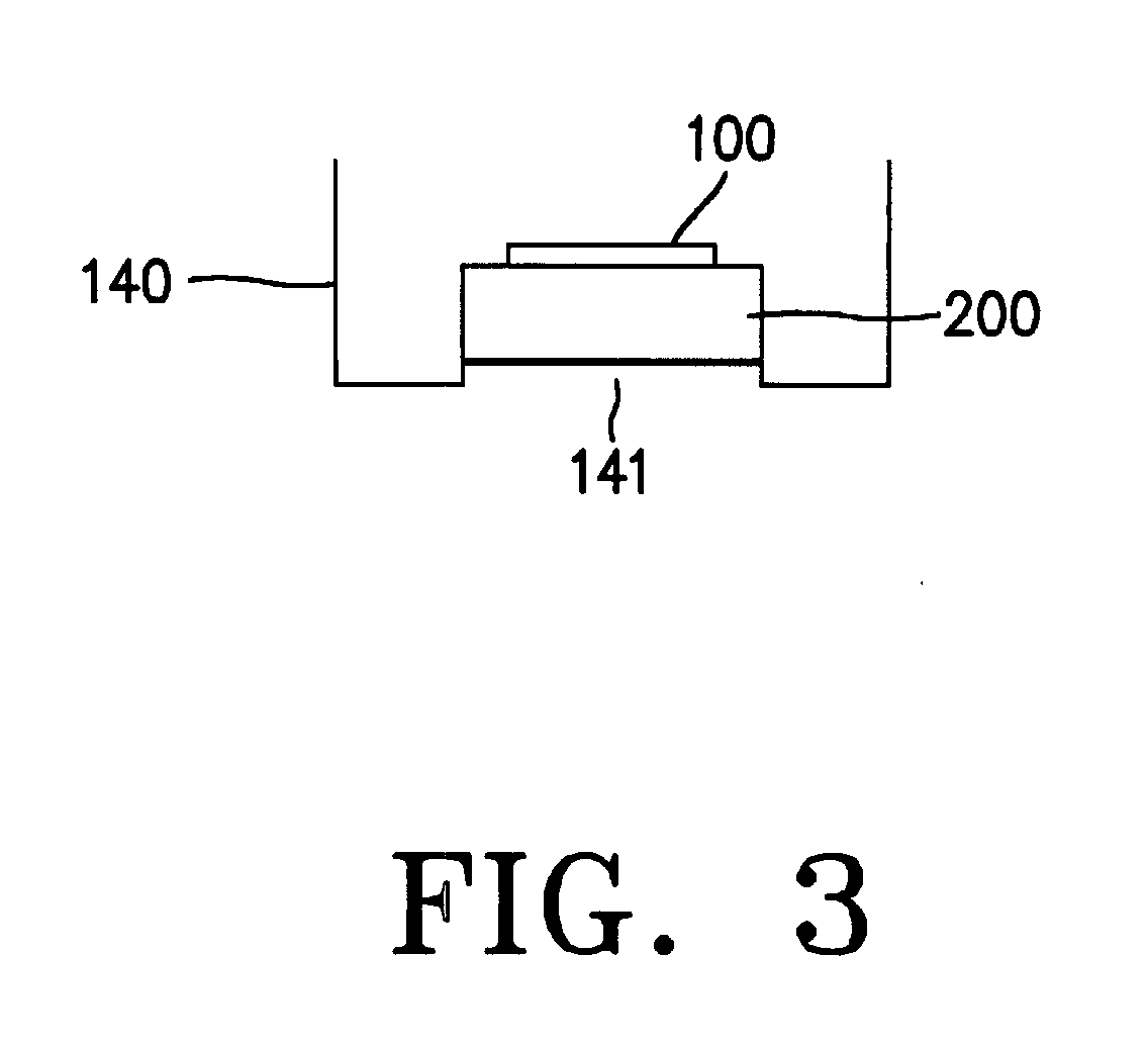
- FIG. 3 is a side elevation view of an optical device module having an integral heat transfer module according to an embodiment of the invention.
- the optical device module of the invention is generally comprised of an optical device 100 which requires temperature control, a heat transfer module 200 and a housing 140.
- the optical device 100 is attached to a heat transfer module 200 via a medium such as thermal grease.
- the heat transfer module 200 is provided according to the characteristics of the invention, and has an outer housing acting as a heat transfer plate of the related art, a heat source capable of heating and a temperature sensor for detecting temperature which are integrally provided. Also, lead wires (not shown) provide the temperature sensor and the heat source with supply voltage and current.
- Such an integral heat transfer module 200 is used to minimize contact portions of each part of the related art to increase simplification of a heat transfer path. A structure of such an integral heat transfer module 200 will be described in more detail in reference to the accompanying drawings.
- FIG. 4 is a cross section of an integral heat transfer module in the optical device module shown in FIG. 3 according to the first embodiment of the invention, the integral heat transfer module 200 employing a heater as the heat source.
- a temperature sensor 201 is provided in the inner upper part of an outer housing 203 of the integral heat transfer module 200, and a heater 202 is provided under the temperature sensor 201.
- the heater 202 can utilize ceramics or hot wires, in which a ceramic heater requires to be attached through soldering after metal plating.
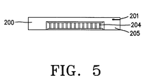
- FIG. 5 is a cross sectional view of an integral heat transfer module of the optical device module shown in FIG. 3 according to the second embodiment of the invention.
- the integral heat transfer module 200 employs a temperature electric cooler (TEC) 204 as the heat source.
- TEC temperature electric cooler
- a temperature sensor 201 is provided in the inner upper part of an outer housing 205 of the integral heat transfer module 200, and a heater 202 is provided under the temperature sensor 201.
- the TEC 204 is constituted as a module of n and p type thermoelectric semiconductors connected electrically in series and thermally in parallel, in which a temperature difference takes place at both sides of the module due to thermoelectric effect when a DC current is applied. As shown in FIG. 5, it is preferred that solder is attached to the upper surface of the TEC 204 and the lower surface is isolated from the outer housing.
- FIGS. 6A and 6B are structural views of integral heat transfer modules in the optical device module shown in FIG. 3 according to the third embodiment of the invention.
- a temperature sensor 201 is provided in the inner upper part of an outer housing 208 of the integral heat transfer module 200, four or five heat pipes 206 are provided under the temperature sensor 201, and a heat source 207 is provided under the heat pipes 206.
- each of the heat pipes 206 internally contains a work fluid in a sealed vessel and utilizes latent heat in which the work fluid transfers heat between both ends of the vessel via phase transformation between gas and liquid phases.
- This scheme provides heat transfer performance which is much more efficient when compared to typical heat transfer devices using work fluids of single phase.
- each heat pipe 206 is comprised of the sealed pipe 206-1, the work fluid and wicks 206-2 inside the vessel.
- the heat pipes are variously classified according to structure type of the wicks 206-2, scheme of returning fluid, geometry of the inside, working temperature and the like.
- the sealed vessel 206-1 and the wicks 206-2 are provided to constitute the each of the heat pipes 206.
- the outer housing of the heat transfer module 200 preferably utilizes a material excellent in heat conductivity.
- the integral heat transfer module 200 as shown in FIGS. 4 to 6B can be attached to the optical device 100 as shown in FIG. 3, and then fixed to the mount 141 of the housing 140.
- four electric wires are required including two wires for the temperature sensor and two wires for the heat source. These four electric wires are pin-treated. Pin holes are formed in portions corresponding to the four pins of the housing 140 so that the pins and the holes fit together. Temperature is monitored and controlled by using these four pins.
- the optical device module of the invention can be obtained by using the integral heat transfer module configured as above.
- the heat transfer module integrally has the heat source and the temperature sensor for reading temperature. Then, the heat transfer path is simplified in packaging the optical device module so that the optical device can avoid performance degradation due to nonuniform temperature distribution, power consumption thereof can be reduced and excellent workability can be ensured.
Landscapes
- Physics & Mathematics (AREA)
- General Physics & Mathematics (AREA)
- Optics & Photonics (AREA)
- Engineering & Computer Science (AREA)
- Automation & Control Theory (AREA)
- Semiconductor Lasers (AREA)
- Cooling Or The Like Of Semiconductors Or Solid State Devices (AREA)
Abstract
An optical device module using an integral heat transfer module (200). The heat transfer
module (200) has an integrally formed heat source (202) and a temperature sensor (201) for reading
temperature. A heat transfer path is simplified in packaging the optical device module, so that
the optical device (100) can avoid performance degradation due to nonuniform temperature
distribution. The amount power consumption can be reduced and excellent workability can
be ensured.
Description
- The present invention generally relates to a technique of manufacturing an optical device module which requires temperature control. More particularly, the present invention relates to an optical device module having a heat transfer medium for overcoming nonuniform temperature distribution.
- In manufacturing an optical device, it is required to control temperature for the stability of wavelength. Also, the temperature gradient in the optical device causes optical loss as well as wavelength variation. Thus, temperature should be uniformly distributed across the whole device. Accordingly, in the prior art, designs of a heat source and a heat dispersing plate have been considered important features.
- A basic prior art method of controlling temperature of the optical device uses the optical device, the heat source and a heat detecting sensor. The heat source and the heat detecting sensor are contacted with the surface of the optical device, and the sensor reads the surface temperature of the device for feedback control.
- However, according to the above-mentioned prior artmethod, temperature distribution of the heat source and temperature fluctuates due to unstable current in the heat source. In order to stabilize the current, a heat transfer plate is installed between the heat source and the device. The transmission of heat flows from the heat source to the device through the heat transfer plate, and the temperature sensor between the heat transfer plate, and the device detects temperature for feedback control.
- FIG. 1 is a schematic perspective view for illustrating such a prior art optical device module, and FIG. 2 is a side structural view of the optical device module shown in FIG. 1.
- Referring to FIG. 2, a typical optical device module is comprised of an
optical device 100 which requires temperature control, atemperature sensor 110, aheat source 130, ahousing 140 and amount 141. In addition, although not shown in the drawings, lead wires are provided to apply voltage or current for heating the heat source. - The thermal contact resistance has the greatest difference according to the amount of contact among the
heat source 130, theheat transfer plate 120 and theoptical device 100. A medium, such as thermal grease, solder and the like, is applied to maintain close contact. In order to obtain the most efficient use of the medium, the contact surfaces should be rubbed for uniform distribution. - However, there are instances when uniform contact still cannot be obtained even with a rubbed contact surfaces containing a medium. In such a case, the temperature is not uniformly dispersed across the whole area of the
heat transfer plate 120, so that temperature distribution is frequently nonuniform across the device. - Also, the
temperature sensor 110 is generally applied as a thermistor or resistance temperature detector (RTD), in which thetemperature sensor 110 is preferably arranged adjacent theoptical device 100 for more accurate temperature detection of theoptical device 100. Here, thetemperature sensor 110 generally has a certain amount of thickness, and thus essentially builds up an insulation layer between theoptical device 100 and theheat transfer plate 120 when placed between theoptical device 100 and theheat transfer plate 120 as shown in FIG. 2. - As described above, the optical device module of the prior art does not provide complete contact among the parts, thereby causing temperature distribution to be nonuniform and efficiency to be degraded. Accordingly, the wavelength features of the optical device are degraded, the optical device can be damaged, and power consumption is increased.
- The present invention has been proposed to solve the foregoing problems of the prior art. The present invention provides an optical device module having excellent workability in which a heat transfer path is simplified by the packaging the optical device module. The present invention permits the optical device to avoid performance degradation due to nonuniform temperature distribution. In addition, in the present invention, power consumption can be reduced over devices in the prior art.
- According to an embodiment of the invention,, it is provided that an optical device module using integral heat transfer module comprises a heat transfer module attached to an optical device and having a heat source for heating, and a temperature sensor for sensing temperature. The heat source and the temperature sensor are integrally formed.
-
- FIG. 1 is a schematic perspective view for illustrating a typical prior art optical device module;
- FIG. 2 is a side structural view of the optical device module shown in FIG. 1;
- FIG. 3 is a side elevation view of an optical device module having an integral heat transfer module according to an embodiment of the invention;
- FIG. 4 is a structural view of an integral heat transfer module in the optical device module shown in FIG. 3 according to a first embodiment of the invention;
- FIG. 5 is a structural view of an integral heat transfer module in the optical device module shown in FIG. 3 according to the a embodiment of the invention; and
- FIGS. 6A and 6B are structural views of integral heat transfer modules in the optical device module shown in FIG. 3 according to a third embodiment of the invention.
-
- FIG. 3 is a side elevation view of an optical device module having an integral heat transfer module according to an embodiment of the invention.
- Referring to FIG. 3, the optical device module of the invention is generally comprised of an
optical device 100 which requires temperature control, aheat transfer module 200 and ahousing 140. Theoptical device 100 is attached to aheat transfer module 200 via a medium such as thermal grease. - The
heat transfer module 200 is provided according to the characteristics of the invention, and has an outer housing acting as a heat transfer plate of the related art, a heat source capable of heating and a temperature sensor for detecting temperature which are integrally provided. Also, lead wires (not shown) provide the temperature sensor and the heat source with supply voltage and current. - Such an integral
heat transfer module 200 is used to minimize contact portions of each part of the related art to increase simplification of a heat transfer path. A structure of such an integralheat transfer module 200 will be described in more detail in reference to the accompanying drawings. - FIG. 4 is a cross section of an integral heat transfer module in the optical device module shown in FIG. 3 according to the first embodiment of the invention, the integral
heat transfer module 200 employing a heater as the heat source. - Referring to FIG. 4, a
temperature sensor 201 is provided in the inner upper part of anouter housing 203 of the integralheat transfer module 200, and aheater 202 is provided under thetemperature sensor 201. In this case, theheater 202 can utilize ceramics or hot wires, in which a ceramic heater requires to be attached through soldering after metal plating. - FIG. 5 is a cross sectional view of an integral heat transfer module of the optical device module shown in FIG. 3 according to the second embodiment of the invention. In this embodiment, the integral
heat transfer module 200 employs a temperature electric cooler (TEC) 204 as the heat source. - Referring to FIG. 5, a
temperature sensor 201 is provided in the inner upper part of anouter housing 205 of the integralheat transfer module 200, and aheater 202 is provided under thetemperature sensor 201. - The TEC 204 is constituted as a module of n and p type thermoelectric semiconductors connected electrically in series and thermally in parallel, in which a temperature difference takes place at both sides of the module due to thermoelectric effect when a DC current is applied. As shown in FIG. 5, it is preferred that solder is attached to the upper surface of the
TEC 204 and the lower surface is isolated from the outer housing. - FIGS. 6A and 6B are structural views of integral heat transfer modules in the optical device module shown in FIG. 3 according to the third embodiment of the invention.
- Referring to FIGS. 6A and 6B, a
temperature sensor 201 is provided in the inner upper part of anouter housing 208 of the integralheat transfer module 200, four or fiveheat pipes 206 are provided under thetemperature sensor 201, and aheat source 207 is provided under theheat pipes 206. - In general, each of the
heat pipes 206 internally contains a work fluid in a sealed vessel and utilizes latent heat in which the work fluid transfers heat between both ends of the vessel via phase transformation between gas and liquid phases. This scheme provides heat transfer performance which is much more efficient when compared to typical heat transfer devices using work fluids of single phase. - As shown in FIG. 6B, each
heat pipe 206 is comprised of the sealed pipe 206-1, the work fluid and wicks 206-2 inside the vessel. The heat pipes are variously classified according to structure type of the wicks 206-2, scheme of returning fluid, geometry of the inside, working temperature and the like. The sealed vessel 206-1 and the wicks 206-2 are provided to constitute the each of theheat pipes 206. Here, the outer housing of theheat transfer module 200 preferably utilizes a material excellent in heat conductivity. - The integral
heat transfer module 200 as shown in FIGS. 4 to 6B can be attached to theoptical device 100 as shown in FIG. 3, and then fixed to themount 141 of thehousing 140. Here, four electric wires are required including two wires for the temperature sensor and two wires for the heat source. These four electric wires are pin-treated. Pin holes are formed in portions corresponding to the four pins of thehousing 140 so that the pins and the holes fit together. Temperature is monitored and controlled by using these four pins. - The optical device module of the invention can be obtained by using the integral heat transfer module configured as above.
- In foregoing the optical device module using the integral heat transfer module of the invention, the heat transfer module integrally has the heat source and the temperature sensor for reading temperature. Then, the heat transfer path is simplified in packaging the optical device module so that the optical device can avoid performance degradation due to nonuniform temperature distribution, power consumption thereof can be reduced and excellent workability can be ensured.
- While the invention has been described about the specific embodiment thereof, a number of modifications and variations may be made without departing the scope of the invention. Therefore, the scope of the invention is not restricted by the foregoing embodiment, but will be defined by the appended claims and the equivalents thereof.
Claims (12)
- An optical device module comprising:an optical device (100) which requires temperature control; andan integrally formed heat transfer module (200) attached to said optical device, said integrally formed heat transfer module (200) including a heat source (202) and a temperature sensor (201) for reading temperature.
- An optical device module according to claim 1, wherein said heat source (202) includes one of ceramics and hot wires.
- An optical device module according to claim 1 or 2, wherein said heat source further comprises a temperature electric cooler (TEC) (204).
- An optical device module according to any of the claims 1 to 3, wherein said heat source comprises heat pipes (206).
- An optical device module according to any of the claims 1 to 4, wherein said temperature sensor (201) and said heat source (202) comprise electric wires which are pin treated.
- An optical device module according to any of the claims 1 to 5, wherein said heat transfer module (200) further comprises an outer housing (203, 205, 208) in which said temperature sensor (201) is arranged, and said heat source (202) is arranged in contact with a bottom surface of said temperature sensor (201).
- An optical device module according to any of the claims 2 to 6, further comprising an outer housing (203, 205, 208), in which said temperature sensor (201) is arranged in an upper portion of said outer housing, (207, 205, 208), and wherein said heat source (202) comprises a ceramic heater arranged in contact with a bottom surface of said ceramic heater.
- An optical device module according to claim 7, wherein said ceramic heater is provided in attachment to said one of ceramics and hot wires by metal plating.
- An optical device module according to claim 3, wherein said TEC comprises a module of n and p thermoelectric semiconductors electrically connected in series, and thermally connected in parallel; and wherein:solder is attached to an upper surface of said TEC (204);said heat transfer module (200) comprises an outer housing (203, 205, 208), anda lower surface of said TEC is isolated from said outer housing (203, 205, 208).
- An optical device according to claim 3, wherein said heat transfer module (200) comprises an outer housing (203, 205, 208), having pin holes formed therein which correspond to the pin-treated electric wires.
- A method for manufacturing an optical device module comprising the steps of:(a) providing an optical device (100) which requires temperature control;(b) integrally forming a heat transfer module (200) attached to said optical device (100) including a heat source (202) and a temperature sensor (201) for reading temperature which are integrally formed.
- The method according to claim 11, further comprising:(c) providing an outer housing (203, 205, 208), having an upper portion in which said temperature sensor (201) is arranged, and said heat source (202) is arranged in contact with a bottom surface of said temperature sensor (201);(d) providing a plurality of heat pipes (206) arranged below said temperature sensor (201), and said heat source (202) being provided below the heat pipes (206) and arranged on a lower portion of said outer housing (203, 205, 208).
Applications Claiming Priority (2)
| Application Number | Priority Date | Filing Date | Title |
|---|---|---|---|
| KR2001004279 | 2001-01-30 | ||
| KR10-2001-0004279A KR100387035B1 (en) | 2001-01-30 | 2001-01-30 | Optical waveguide module using unified heat conducting module |
Publications (1)
| Publication Number | Publication Date |
|---|---|
| EP1227352A1 true EP1227352A1 (en) | 2002-07-31 |
Family
ID=19705097
Family Applications (1)
| Application Number | Title | Priority Date | Filing Date |
|---|---|---|---|
| EP01122972A Withdrawn EP1227352A1 (en) | 2001-01-30 | 2001-09-25 | Optical device module using integral heat transfer module |
Country Status (4)
| Country | Link |
|---|---|
| US (1) | US6677555B2 (en) |
| EP (1) | EP1227352A1 (en) |
| JP (1) | JP3672520B2 (en) |
| KR (1) | KR100387035B1 (en) |
Cited By (3)
| Publication number | Priority date | Publication date | Assignee | Title |
|---|---|---|---|---|
| EP1398655A1 (en) * | 2002-09-06 | 2004-03-17 | Agfa-Gevaert AG | Thermal conditioning for optical module |
| DE102007034485A1 (en) * | 2007-07-20 | 2009-01-22 | Oc Oerlikon Balzers Ag | Device, particularly heating device, has optical element with surface and is arranged at thermally conductive mounting plate, where mounting plate is thermally conductive connected with optical element over total surface |
| CN114824051A (en) * | 2021-01-29 | 2022-07-29 | 台湾积体电路制造股份有限公司 | Semiconductor structure and method for manufacturing semiconductor structure |
Families Citing this family (4)
| Publication number | Priority date | Publication date | Assignee | Title |
|---|---|---|---|---|
| US20050074040A1 (en) * | 2003-10-03 | 2005-04-07 | Spence David E. | Diamond cooled laser gain assembly |
| US7157664B2 (en) * | 2005-03-29 | 2007-01-02 | Scientific-Atlanta, Inc. | Laser heater assembly |
| EP2343586A1 (en) * | 2009-12-30 | 2011-07-13 | Nederlandse Organisatie voor toegepast -natuurwetenschappelijk onderzoek TNO | Shape stabilized mirror module and method to stabilize a reflective element. |
| KR102213714B1 (en) | 2020-03-18 | 2021-02-09 | (주)명성라이픽스 | Touch sensing system to prevent malfunctions |
Citations (5)
| Publication number | Priority date | Publication date | Assignee | Title |
|---|---|---|---|---|
| US5522225A (en) * | 1994-12-19 | 1996-06-04 | Xerox Corporation | Thermoelectric cooler and temperature sensor subassembly with improved temperature control |
| US6043982A (en) * | 1998-04-01 | 2000-03-28 | Raytheon Company | Integrated circuit package having a thermoelectric cooling element therein |
| EP0997991A2 (en) * | 1998-10-30 | 2000-05-03 | Litton Systems, Inc., Delaware | Temperature-controlled microchip laser assembly and associated submount assembly |
| US6091837A (en) * | 1995-04-11 | 2000-07-18 | Dinh; Ngoc Minh | Sensor for acquiring a fingerprint image based on heat transfer |
| US6098408A (en) * | 1998-11-11 | 2000-08-08 | Advanced Micro Devices | System for controlling reflection reticle temperature in microlithography |
Family Cites Families (18)
| Publication number | Priority date | Publication date | Assignee | Title |
|---|---|---|---|---|
| US3940621A (en) * | 1975-01-21 | 1976-02-24 | Nasa | Heat transfer device |
| US4739382A (en) * | 1985-05-31 | 1988-04-19 | Tektronix, Inc. | Package for a charge-coupled device with temperature dependent cooling |
| US5070936A (en) * | 1991-02-15 | 1991-12-10 | United States Of America As Represented By The Secretary Of The Air Force | High intensity heat exchanger system |
| US5363391A (en) * | 1992-04-24 | 1994-11-08 | Hughes Aircraft Company | Conductive face-cooled laser crystal |
| US5523563A (en) * | 1994-08-12 | 1996-06-04 | E. I. Du Pont De Nemours And Company | Apparatus for controlling the temperature of a near-infrared analyzer |
| JPH0921929A (en) * | 1995-07-06 | 1997-01-21 | Oki Electric Ind Co Ltd | Optical module |
| JPH09211272A (en) * | 1996-01-31 | 1997-08-15 | Furukawa Electric Co Ltd:The | Optical module |
| JPH10123340A (en) * | 1996-10-23 | 1998-05-15 | Hitachi Cable Ltd | Waveguide type optical module |
| JPH10190141A (en) * | 1996-12-20 | 1998-07-21 | Fujitsu Ltd | Optical semiconductor module |
| JP2000131539A (en) * | 1998-10-22 | 2000-05-12 | Hitachi Cable Ltd | Waveguide type optical module |
| JP2000155227A (en) * | 1998-11-19 | 2000-06-06 | Hitachi Cable Ltd | Waveguide type optical module |
| KR100322127B1 (en) * | 1999-01-18 | 2002-02-04 | 윤종용 | AWG multiplexer |
| US6184504B1 (en) * | 1999-04-13 | 2001-02-06 | Silicon Thermal, Inc. | Temperature control system for electronic devices |
| IT1311257B1 (en) * | 1999-10-26 | 2002-03-04 | Cselt Centro Studi Lab Telecom | PROCEDURE AND DEVICE FOR THE THERMAL CONDITIONING OF THE ELECTRONIC COMPONENTS. |
| JP2001133105A (en) * | 1999-11-02 | 2001-05-18 | Smc Corp | Pipe cooler and small temperature controller using the pipe cooler |
| JP4430769B2 (en) * | 1999-12-09 | 2010-03-10 | 信越化学工業株式会社 | Ceramic heating jig |
| JP3228924B2 (en) * | 2000-01-21 | 2001-11-12 | イビデン株式会社 | Ceramic heater for semiconductor manufacturing and inspection equipment |
| KR100369811B1 (en) * | 2001-01-30 | 2003-01-29 | 삼성전자 주식회사 | Optical waveguide module using heat conducting element by means of phase change |
-
2001
- 2001-01-30 KR KR10-2001-0004279A patent/KR100387035B1/en not_active Expired - Fee Related
- 2001-08-23 US US09/935,825 patent/US6677555B2/en not_active Expired - Lifetime
- 2001-09-25 EP EP01122972A patent/EP1227352A1/en not_active Withdrawn
- 2001-10-26 JP JP2001329830A patent/JP3672520B2/en not_active Expired - Fee Related
Patent Citations (5)
| Publication number | Priority date | Publication date | Assignee | Title |
|---|---|---|---|---|
| US5522225A (en) * | 1994-12-19 | 1996-06-04 | Xerox Corporation | Thermoelectric cooler and temperature sensor subassembly with improved temperature control |
| US6091837A (en) * | 1995-04-11 | 2000-07-18 | Dinh; Ngoc Minh | Sensor for acquiring a fingerprint image based on heat transfer |
| US6043982A (en) * | 1998-04-01 | 2000-03-28 | Raytheon Company | Integrated circuit package having a thermoelectric cooling element therein |
| EP0997991A2 (en) * | 1998-10-30 | 2000-05-03 | Litton Systems, Inc., Delaware | Temperature-controlled microchip laser assembly and associated submount assembly |
| US6098408A (en) * | 1998-11-11 | 2000-08-08 | Advanced Micro Devices | System for controlling reflection reticle temperature in microlithography |
Cited By (3)
| Publication number | Priority date | Publication date | Assignee | Title |
|---|---|---|---|---|
| EP1398655A1 (en) * | 2002-09-06 | 2004-03-17 | Agfa-Gevaert AG | Thermal conditioning for optical module |
| DE102007034485A1 (en) * | 2007-07-20 | 2009-01-22 | Oc Oerlikon Balzers Ag | Device, particularly heating device, has optical element with surface and is arranged at thermally conductive mounting plate, where mounting plate is thermally conductive connected with optical element over total surface |
| CN114824051A (en) * | 2021-01-29 | 2022-07-29 | 台湾积体电路制造股份有限公司 | Semiconductor structure and method for manufacturing semiconductor structure |
Also Published As
| Publication number | Publication date |
|---|---|
| JP3672520B2 (en) | 2005-07-20 |
| US20020101891A1 (en) | 2002-08-01 |
| US6677555B2 (en) | 2004-01-13 |
| KR20020063692A (en) | 2002-08-05 |
| KR100387035B1 (en) | 2003-06-12 |
| JP2002232065A (en) | 2002-08-16 |
Similar Documents
| Publication | Publication Date | Title |
|---|---|---|
| AU736484B2 (en) | Improvements in thermal cycler for PCR | |
| US7645070B2 (en) | Thermal cycler for PCR | |
| WO1998043740A9 (en) | Improvements in thermal cycler for pcr | |
| US6677555B2 (en) | Optical device module using integral heat transfer module | |
| JPH1168173A (en) | Heat exchanger using thermoelectric module | |
| GB2333397A (en) | Thermoelectric temperature control of corrosive fluids | |
| KR100369811B1 (en) | Optical waveguide module using heat conducting element by means of phase change | |
| EP1127619B1 (en) | Assembly for thermal cycler for PCR | |
| EP1386666B1 (en) | Improvements in thermal cycler for pcr | |
| US20260118416A1 (en) | Chuck | |
| JPH04213103A (en) | Thermostatic device | |
| WO1999048139A2 (en) | Apparatus for reducing heat loss | |
| CA2464973A1 (en) | Thermal cycler for pcr |
Legal Events
| Date | Code | Title | Description |
|---|---|---|---|
| PUAI | Public reference made under article 153(3) epc to a published international application that has entered the european phase |
Free format text: ORIGINAL CODE: 0009012 |
|
| 17P | Request for examination filed |
Effective date: 20010925 |
|
| AK | Designated contracting states |
Kind code of ref document: A1 Designated state(s): AT BE CH CY DE DK ES FI FR GB GR IE IT LI LU MC NL PT SE TR |
|
| AX | Request for extension of the european patent |
Free format text: AL;LT;LV;MK;RO;SI |
|
| AKX | Designation fees paid |
Designated state(s): DE FR GB |
|
| 17Q | First examination report despatched |
Effective date: 20030709 |
|
| STAA | Information on the status of an ep patent application or granted ep patent |
Free format text: STATUS: THE APPLICATION IS DEEMED TO BE WITHDRAWN |
|
| 18D | Application deemed to be withdrawn |
Effective date: 20070331 |